Äîêóìåíòàöèÿ è îïèñàíèÿ www.docs.chipfind.ru
1
LTC1151
Dual
±
15V Zero-Drift
Operational Amplifier
15V
15V
+
15V
0.1
µ
F
6
5
8
1/2
LTC1151
7
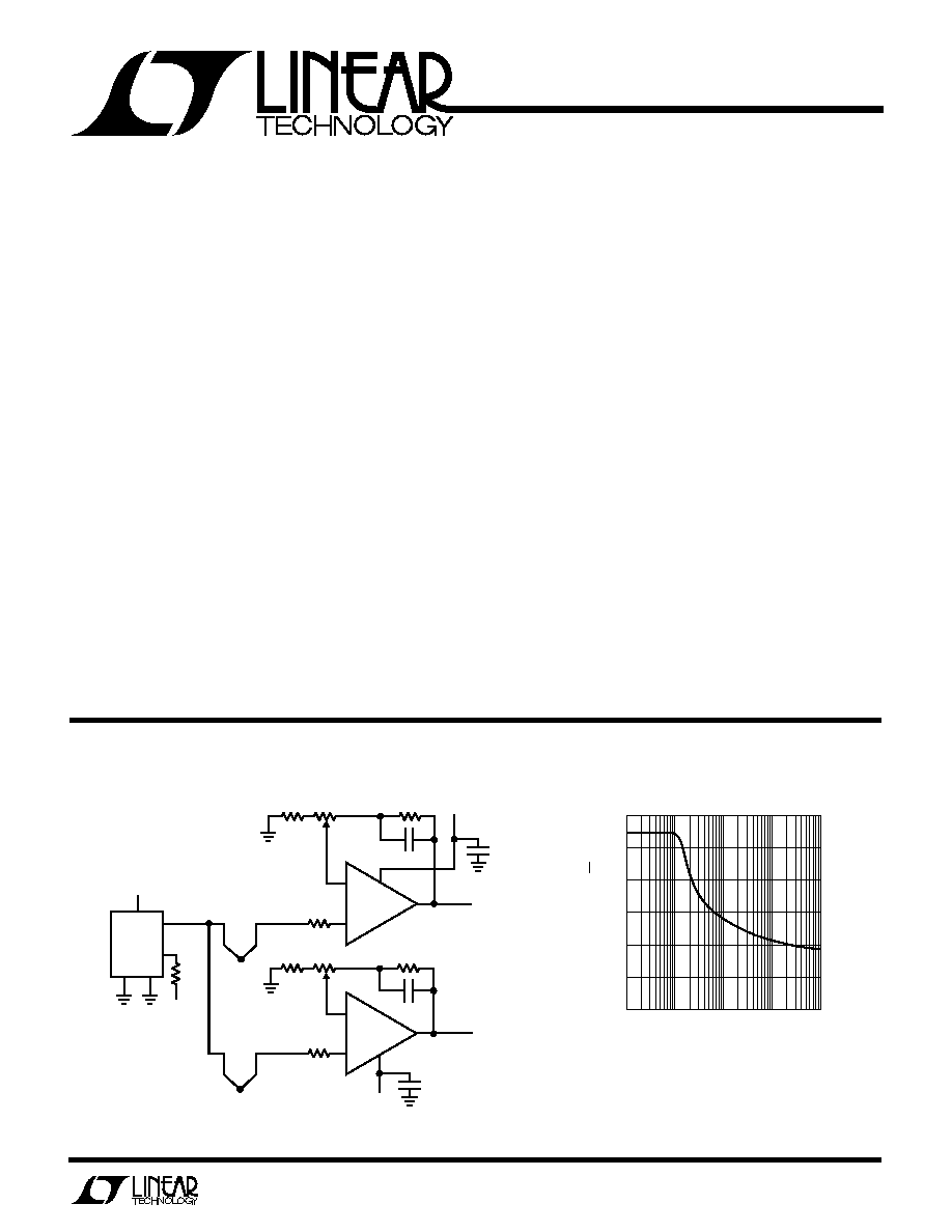
OUTPUT A
100mV/°C
1151 TA01
240k
51
100
*
0.1
µ
F
2k
LT1025
15V
470k
V
IN
K
V
O
R
GND
7
3
+
+
TYPE K
0.1
µ
F
2
3
4
1/2
LTC1151
1
OUTPUT B
100mV/°C
240k
51
100
*
0.1
µ
F
2k
+
5
4
TYPE K
* FULL SCALE TRIM: TRIM FOR 10.0V OUTPUT
WITH THERMOCOUPLE AT 100°C
U
A
O
PPLICATI
TYPICAL
D
U
ESCRIPTIO
S
FEATURE
The LTC1151 is a high voltage, high performance dual
zero-drift operational amplifier. The two sample-and-hold
capacitors per amplifier required externally by other chop-
per amplifiers are integrated on-chip. The LTC1151 also
incorporates proprietary high voltage CMOS structures
which allow operation at up to 36V total supply voltage.
The LTC1151 has a typical offset voltage of 0.5
µ
V,
drift of 0.01
µ
V/
°
C, 0.1Hz to 10Hz input noise voltage of
1.5
µ
V
P-P
, and a typical voltage gain of 140dB. It has a slew
rate of 3V/
µ
s and a gain-bandwidth product of 2.5MHz
with a supply current of 0.9mA per amplifier. Overload
recovery times from positive and negative saturation are
3ms and 20ms, respectively.
The LTC1151 is available in a standard 8-lead plastic DIP
package as well as a 16-lead wide body SO. The LTC1151
is pin compatible with industry-standard dual op amps
and runs from standard
±
15V supplies, allowing it to plug
in to most standard bipolar op amp sockets while offering
significant improvement in DC performance.
U
S
A
O
PPLICATI
s
Strain Gauge Amplifiers
s
Instrumentation Amplifiers
s
Electronic Scales
s
Medical Instrumentation
s
Thermocouple Amplifiers
s
High Resolution Data Acquisition
s
Maximum Offset Voltage Drift: 0.05
µ
V/
°
C
s
High Voltage Operation:
±
18V
s
No External Components Required
s
Maximum Offset Voltage: 5
µ
V
s
Low Noise: 1.5
µ
V
P-P
(0.1Hz to 10Hz)
s
Minimum Voltage Gain: 125dB
s
Minimum CMRR: 106dB
s
Minimum PSRR: 110dB
s
Low Supply Current: 0.9mA/Amplifier
s
Single Supply Operation: 4.75V to 36V
s
Input Common-Mode Range Includes Ground
s
Typical Overload Recovery Time: 20ms
Noise Spectrum
±
15V Dual Thermocouple Amplifier
FREQUENCY (Hz)
10
NOISE VOLTAGE (nV/
Hz)
20
30
40
60
1
100
1k
10k
1151 TA02
0
10
50
LTC1151
2
Total Supply Voltage (V
+
to V
) ............................. 36V
Input Voltage (Note 2) .......... (V
+
+ 0.3V) to (V
0.3V)
Output Short Circuit Duration ......................... Indefinite
Burn-In Voltage ...................................................... 36V
(Note 1)
A
U
G
W
A
W
U
W
A
R
BSOLUTE
XI
TI
S
Operating Temperature Range
LTC1151C............................................... 0
°
C to 70
°
C
Storage Temperature Range ................ 65
°
C to 150
°
C
Lead Temperature (Soldering, 10 sec)................. 300
°
C
W
U
U
PACKAGE/ORDER I FOR ATIO
T
JMAX
= 110
°
C,
JA
= 130
°
C/ W
ORDER PART
NUMBER
ORDER PART
NUMBER
T
JMAX
= 110
°
C,
JA
= 200
°
C/ W
LTC1151CS
LTC1151CN8
1
2
3
4
8
7
6
5
TOP VIEW
OUT A
IN A
+IN A
V
V
+
OUT B
IN B
+IN B
N8 PACKAGE
8-LEAD PLASTIC DIP
ELECTRICAL C
C
HARA TERISTICS
V
S
=
±
15V, T
A
= Operating Temperature Range, unless otherwise specified.
LTC1151C
PARAMETER
CONDITIONS
MIN
TYP
MAX
UNITS
Input Offset Voltage
T
A
= 25
°
C (Note 3)
±
0.5
±
5
µ
V
Average Input Offset Drift
(Note 3)
q
±
0.01
±
0.05
µ
V/
°
C
Long Term Offset Voltage Drift
50
nV/
mo
Input Offset Current
T
A
= 25
°
C
±
20
±
200
pA
q
±
0.5
nA
Input Bias Current
T
A
= 25
°
C
±
15
±
100
pA
q
±
0.5
nA
Input Noise Voltage
R
S
= 100
, 0.1Hz to 10Hz
1.5
µ
V
P-P
R
S
= 100
, 0.1Hz to 1Hz
0.5
µ
V
P-P
Input Noise Current
f = 10Hz (Note 4)
2.2
fA/
Hz
Input Voltage Range
Positive
q
12
13.2
V
Negative
q
15
15.3
V
Common-Mode Rejection Ratio
V
CM
= V
to 12V
q
106
130
dB
Power Supply Rejection Ratio
V
S
=
±
2.375V to
±
16V
q
110
130
dB
Large-Signal Voltage Gain
R
L
= 10k, V
OUT
=
±
10V
q
125
140
dB
NC
NC
OUT A
IN A
+IN A
V
NC
NC
NC
NC
V
+
OUT B
IN B
+IN B
NC
NC
TOP VIEW
S PACKAGE
16-LEAD PLASTIC SOL
1
2
3
4
5
6
7
8
16
15
14
13
12
11
10
9
3
LTC1151
ELECTRICAL C
C
HARA TERISTICS
V
S
=
±
15V, T
A
= Operating Temperature Range, unless otherwise specified.
LTC1151C
PARAMETER
CONDITIONS
MIN
TYP
MAX
UNITS
Maximum Output Voltage Swing
R
L
= 10k, T
A
= 25
°
C
±
13.5
±
14.50
V
R
L
= 10k
q
+10.5/13.5
V
R
L
= 100k
±
14.95
V
Slew Rate
R
L
= 10k, C
L
= 50pF
2.5
V/
µ
s
Gain-Bandwidth Product
2
MHz
Supply Current per Amplifier
No Load, T
A
= 25
°
C
0.9
1.5
mA
No Load
q
2.0
mA
Internal Sampling Frequency
1000
Hz
Input Offset Voltage
T
A
= 25
°
C (Note 3)
±
0.05
±
5
µ
V
Average Input Offset Drift
(Note 3)
q
±
0.01
±
0.05
µ
V/
°
C
Long Term Offset Voltage Drift
50
nV/
mo
Input Offset Current
T
A
= 25
°
C
±
10
100
pA
Input Bias Current
T
A
= 25
°
C
±
5
50
pA
Input Noise Voltage
R
S
= 100
, 0.1Hz to 10Hz
2.0
µ
V
P-P
R
S
= 100
, 0.1Hz to 1Hz
0.7
µ
V
P-P
Input Noise Current
f = 10Hz (Note 4)
1.3
fA/
Hz
Input Voltage Range
Positive
2.7
3.2
V
Negative
0
0.3
V
Common-Mode Rejection Ratio
V
CM
= 0V to 2.7V
110
dB
Power Supply Rejection Ratio
V
S
=
±
2.375V to
±
16V
q
110
130
dB
Large-Signal Voltage Gain
R
L
= 10k, V
OUT
= 0.3V to 4.5V
q
115
140
dB
Maximum Output Voltage Swing
R
L
= 10k to GND
4.85
V
R
L
= 100k to GND
4.97
V
Slew Rate
R
L
= 10k, C
L
= 50pF
1.5
V/
µ
s
Gain Bandwidth Product
1.5
MHz
Supply Current per Amplifier
No Load, T
A
= 25
°
C
0.5
1.0
mA
q
1.5
mA
Internal Sampling Frequency
750
Hz
The
·
denotes the specifications which apply over the full operating
temperature range.
Note 1: Absolute Maximum Ratings are those values beyond which life of
the device may be impaired.
Note 2: Connecting any terminal to voltages greater than V
+
or less than
V
may cause destructive latch-up. It is recommended that no sources
operating from external supplies be applied prior to power-up of the
LTC1151.
Note 3: These parameters are guaranteed by design. Thermocouple
effects preclude measurement of these voltage levels in high speed
automatic test systems. V
OS
is measured to a limit determined by test
equipment capability.
Note 4: Current Noise is calculated from the formula:
I
N
=
(2q · I
b
)
where q = 1.6
×
10
19
Coulomb.
V
S
= 5V, T
A
= Operating Temperature Range, unless otherwise specified.
LTC1151
4
C
C
HARA TERISTICS
U
W
A
TYPICAL PERFOR
CE
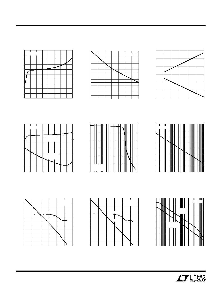
Supply Current vs Supply Voltage
Common-Mode Input Voltage
Range vs Supply Voltage
CMRR vs Frequency
Output Short-Circuit Current vs
Supply Voltage
Gain and Phase vs Frequency
PSRR vs Frequency
TOTAL SUPPLY VOLTAGE (V)
4
0
TOTAL SUPPLY CURRENT (mA)
1.0
2.5
12
20
24
1151 G01
0.5
2.0
1.5
8
16
28
32
36
T
A
= 25°C
SUPPLY VOLTAGE (V)
0
15
COMMON-MODE RANGE (V)
10
5
0
5
10
15
±2.5
±5.0
±10.0
±7.5
1151 G03
±15.0
±12.5
T
A
= 25°C
FREQUENCY (Hz)
40
CMRR (dB)
60
100
140
160
1
10k
100k
1k
1151 G06
0
10
120
80
20
100
V
S
= ±15V
TOTAL SUPPLY VOLTAGE, V
+
TO V
(V)
4
15
SHORT-CIRCUIT OUTPUT CURRENT (mA)
12
9
3
0
4
6
12
20
28
36
1151 G04
2
6
8
16
24
32
T
A
= 25°C
V
OUT
= V
I
SOURCE
V
OUT
= V
+
I
SINK
FREQUENCY (Hz)
10
0
GAIN (dB)
20
40
60
1151 G07
80
100
100
1k
10k
100k
1M
10M
PHASE (DEG)
135
90
45
0
45
PHASE
GAIN
V
S
= ±15V
C
L
= 100pF
80
PSRR (dB)
100
120
140
160
1
100
1k
10k
1151 G09
60
10
20
40
100k
0
POSITIVE
SUPPLY
NEGATIVE
SUPPLY
FREQUENCY (Hz)
V
S
= ±15V
FREQUENCY (Hz)
10
0
GAIN (dB)
20
40
60
1151 G08
80
100
100
1k
10k
100k
1M
10M
PHASE (DEG)
135
90
45
0
45
PHASE
GAIN
V
S
= ±2.5V
C
L
= 100pF
Gain and Phase vs Frequency
FREQUENCY (Hz)
20
OUTPUT VOLTAGE (V
P-P
)
25
30
100
10k
100k
1M
1151 G05
15
1k
5
10
0
V
S
= ±15V
R
L
= 10k
Undistorted Output Swing vs
Frequency
Supply Current vs Temperature
TEMPERATURE (°C)
0
1.75
2.00
40
1151 G02
1.50
10
30
70
1.25
TOTAL SUPPLY CURRENT (mA)
20
50
60
V
S
= ±15V
5
LTC1151
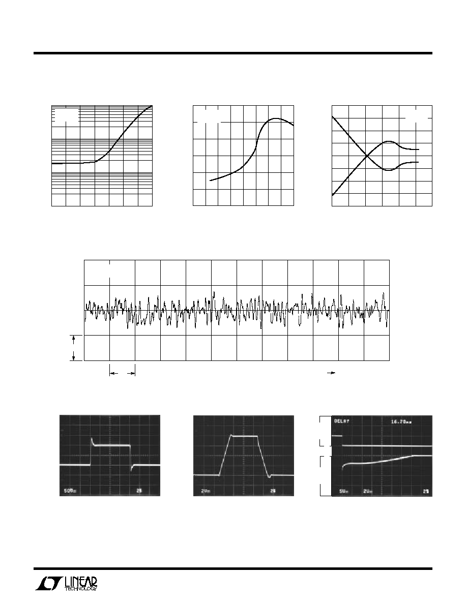
0.1Hz to 10Hz Noise
Negative Overload Recovery
Input Bias Current Magnitude vs
Supply Voltage
Large-Signal Transient Response
INPUT COMMON-MODE VOLTAGE (V)
15
60
INPUT BIAS CURRENT (pA)
5
5
1151 G12
15
10
0
10
45
30
15
0
15
30
45
60
I
B
+I
B
V
S
= 15V
T
A
= 25°C
Input Bias Current vs
Input Common-Mode Voltage
TEMPERATURE (°C)
50
1
INPUT BIAS CURRENT (pA)
10
100
1000
25
0
125
1151 G10
25
50
75
100
V
CM
= 0
V
S
= ±15V
C
C
HARA TERISTICS
U
W
A
TYPICAL PERFOR
CE
Input Bias Current Magnitude vs
Temperature
SUPPLY VOLTAGE (V)
0
0
INPUT BIAS CURRENT (pA)
3
6
9
12
15
1151 G11
18
±2
±4
±6
±8
±10 ±12 ±14 ±16
T
A
= 25°C
V
CM
= 0V
1s
10s
1
µ
V
1151 G13
V
S
= ±15V
T
A
= 25°C
Small-Signal Transient Response
V
S
=
±
15V, A
V
= 1
C
L
= 100pF, R
L
= 10k
V
S
=
±
15V, A
V
= 1
C
L
= 100pF, R
L
= 10k
2ms/DIV
2ms/DIV
2ms/DIV
V
S
=
±
15V, A
V
= 100
NOTE: POSITIVE OVERLOAD RECOVERY IS
TYPICALLY 3ms.
5
2V
/
DIV
0
0
2V
/
DIV
50mV
/
DIV
1151 G14
1151 G15
5V
/
DIV
1151 G16