 | ÐлекÑÑоннÑй компоненÑ: LTC1152C | СкаÑаÑÑ:  PDF PDF  ZIP ZIP |
Äîêóìåíòàöèÿ è îïèñàíèÿ www.docs.chipfind.ru
1
LTC1152
Rail-to-Rail Input
Rail-to-Rail Output
Zero-Drift Op Amp
S
FEATURE
s
Input Common-Mode Range Includes Both Rails
s
Output Swings Rail to Rail
s
Output Will Drive 1k
Load
s
No External Components Required
s
Input Offset Voltage: 10
µ
V Max
s
Input Offset Drift: 100nV/
°
C Max
s
Minimum CMRR: 115dB
s
Supply Current: 3.0mA Max
s
Shutdown Pin Drops Supply Current to 5
µ
A Max
s
Output Configurable to Drive Any Capacitive Load
s
Operates from 2.7V to 14V Total Supply Voltage
U
S
A
O
PPLICATI
s
Rail-to-Rail Amplifiers and Buffers
s
High Resolution Data Acquisition Systems
s
Supply Current Sensing in Either Rail
s
Low Supply Voltage Transducer Amplifiers
s
High Accuracy Instrumentation
s
Single Negative Supply Operation
D
U
ESCRIPTIO
The LTC
®
1152 is a high performance, low power zero-drift
op amp featuring an input stage that common modes to
both power supply rails and an output stage that provides
rail-to-rail swing, even into heavy loads. The wide input
common-mode range is achieved with a high frequency
on-board charge pump. This technique eliminates the
crossover distortion and limited CMRR imposed by com-
peting technologies. The LTC1152 is a C-Load
TM
of amp,
enabling it to drive any capacitive load.
The LTC1152 shares the excellent DC performance specs
of LTC's other zero-drift amplifiers. Typical offset voltage
is 1
µ
V and typical offset drift is 10nV/
°
C. CMRR and PSRR
are 130dB and 120dB and open-loop gain is 130dB. Input
noise voltage is 2
µ
V
P-P
from 0.1Hz to 10Hz. Gain-band-
width product is 0.7MHz and slew rate is 0.5V/
µ
s, all with
supply current of 3.0mA max over temperature. The
LTC1152 also includes a shutdown feature which drops
supply current to 1
µ
A and puts the output stage in a high
impedance state.
The LTC1152 is available in 8-pin PDIP and 8-pin SO
packages and uses the standard op amp pinout, allowing
it to be a plug-in replacement for many standard op amps.
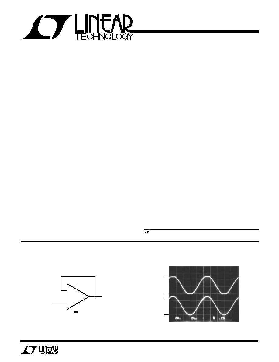
5V
0V
1152 TA02
Input and Output Waveforms
Rail-to-Rail Buffer
V
OUT
2V/DIV
0V
5V
V
IN
2V/DIV
U
A
O
PPLICATI
TYPICAL
, LTC and LT are registered trademarks of Linear Technology Corporation.
C-Load is trademark of Linear Technology Corporation.
+
OUT
7
6
4
3
2
LTC1152
5V
IN
1152 TA01
2
LTC1152
A
U
G
W
A
W
U
W
A
R
BSOLUTE
XI
TI
S
W
U
U
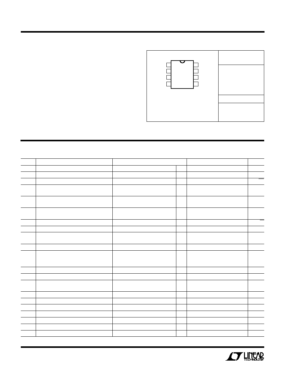
PACKAGE/ORDER I FOR ATIO
ORDER PART
NUMBER
LTC1152CN8
LTC1152CS8
LTC1152IN8
LTC1152IS8
V
S
= 5V, T
A
= operating temperature range, unless otherwise specified.
Consult factory for Military grade parts.
1152
1152I
S8 PART MARKING
Total Supply Voltage (V
+
to V
) ............................. 14V
Input Voltage ............................ V
+
+ 0.3V to V
0.3V
Output Short-Circuit Duration (Pin 6) ............. Indefinite
Operating Temperature Range
LTC1152C............................................... 0
°
C to 70
°
C
LTC1152I .......................................... 40
°
C to 85
°
C
Storage Temperature Range ................ 65
°
C to 150
°
C
Lead Temperature (Soldering, 10 sec)................. 300
°
C
ELECTRICAL C
C
HARA TERISTICS
SYMBOL
PARAMETER
CONDITIONS
MIN
TYP
MAX
UNITS
V
OS
Input Offset Voltage
T
A
= 25
°
C (Note 1)
±
1
±
10
µ
V
V
OS
Average Input Offset Drift
(Note 1)
q
±
10
±
100
nV/
°
C
Long-Term Offset Drift
±
50
nV/
Mo
I
B
Input Bias Current
T
A
= 25
°
C (Note 2)
±
10
±
100
pA
q
±
1000
pA
I
OS
Input Offset Current
T
A
= 25
°
C (Note 2)
±
20
±
200
pA
q
±
500
pA
e
n
Input Noise Voltage (Note 3)
R
S
= 100
, 0.1Hz to 10Hz
2
3
µ
V
P-P
R
S
= 100
, 0.1Hz to 1Hz
0.5
1
µ
V
P-P
i
n
Input Noise Current
f = 10Hz
0.6
fA/
Hz
CMRR
Common-Mode Rejection Ratio
V
CM
= 0V to 5V
q
115
130
dB
PSRR
Power Supply Rejection Ratio
V
S
= 3V to 12V
110
120
dB
q
105
dB
A
VOL
Large-Signal Voltage Gain
R
L
= 10k, V
OUT
= 0.5V to 4.5V
q
110
130
dB
V
OUT
Maximum Output Voltage Swing (Note 4)
R
L
= 1k, V
S
= Single 5V
q
4.0
4.4
V
R
L
= 1k, V
S
=
±
2.5V
q
±
2.0
2.2
V
R
L
= 100k, V
S
=
±
2.5V
±
2.49
V
SR
Slew Rate
R
L
= 10k, C
L
= 50pF, V
S
=
±
2.5V
0.5
V/
µ
s
GBW
Gain-Bandwidth Product
R
L
= 10k, C
L
= 50pF, V
S
=
±
2.5V
0.7
MHz
I
S
Supply Current
No Load
q
2.2
3.0
mA
Shutdown = 0V
q
1
5
µ
A
I
OSD
Output Leakage Current
Shutdown = 0V
q
±
10
±
100
nA
V
CP
Charge Pump Output Voltage
I
CP
= 0
7.3
V
V
IL
Shutdown Pin Input Low Voltage
2.5
V
V
IH
Shutdown Pin Input High Voltage
4
V
I
IN
Shutdown Pin Input Current
V
SHDN
= 0V
q
1
5
µ
A
f
CP
Internal Charge Pump Frequency
T
A
= 25
°
C
4.7
MHz
f
SMPL
Internal Sampling Frequency
T
A
= 25
°
C
2.3
kHz
T
JMAX
= 110
°
C,
JA
= 130
°
C/ W (N8)
T
JMAX
= 110
°
C,
JA
= 200
°
C/ W (S8)
1
2
3
4
8
7
6
5
TOP VIEW
SHDN
IN
+IN
V
CP
V
+
OUT
COMP
N8 PACKAGE
8-LEAD PDIP
S8 PACKAGE
8-LEAD PLASTIC SO
3
LTC1152
V
S
= 3V, T
A
= operating temperature range, unless otherwise specified.
ELECTRICAL C
C
HARA TERISTICS
SYMBOL
PARAMETER
CONDITIONS
MIN
TYP
MAX
UNITS
V
OS
Input Offset Voltage
T
A
= 25
°
C (Note 1)
±
1
±
10
µ
V
V
OS
Average Input Offset Drift
(Note 1)
q
±
10
±
100
nV/
°
C
I
B
Input Bias Current
T
A
= 25
°
C (Note 2)
±
5
±
100
pA
q
±
1000
pA
I
OS
Input Offset Current
T
A
= 25
°
C (Note 2)
±
10
±
200
pA
q
±
500
pA
e
n
Input Noise Voltage (Note 3)
R
S
= 100
, 0.1Hz to 10Hz
2
µ
V
P-P
R
S
= 100
, 0.1Hz to 1Hz
0.75
µ
V
P-P
i
n
Input Noise Current
f = 10Hz
0.6
fA/
Hz
CMRR
Common-Mode Rejection Ratio
V
CM
= 0V to 3V
q
130
dB
A
VOL
Large-Signal Voltage Gain
R
L
= 10k, V
OUT
= 0.5V to 2.5V
q
106
130
dB
V
OUT
Maximum Output Voltage Swing (Note 4)
R
L
= 1k, V
S
= Single 3V
q
2.0
2.5
V
R
L
= 100k, V
S
=
±
1.5V
±
1.48
V
SR
Slew Rate
R
L
= 10k, C
L
= 50pF, V
S
=
±
1.5V
0.4
V/
µ
s
GBW
Gain-Bandwidth Product
R
L
= 10k, C
L
= 50pF, V
S
=
±
1.5V
0.5
MHz
I
S
Supply Current
No Load
q
1.8
2.5
mA
Shutdown = 0V
q
1
5
µ
A
I
OSD
Output Leakage Current
Shutdown = 0V
q
±
10
nA
V
CP
Charge Pump Output Voltage
I
CP
= 0
4.5
V
V
IL
Shutdown Pin Input Low Voltage
1.2
V
V
IH
Shutdown Pin Input High Voltage
2.3
V
I
IN
Shutdown Pin Input Current
V
SHDN
= 0V
1
µ
A
f
CP
Internal Charge Pump Frequency
T
A
= 25
°
C
4.2
MHz
f
SMPL
Internal Sampling Frequency
T
A
= 25
°
C
2.1
kHz
filter at 0.1Hz. Contact LTC factory for sample tested or 100% tested noise
parts.
Note 4: All output swing measurements are taken with the load resistor
connected from output to ground. For single supply tests, only the positive
swing is specified (negative swing will be 0V due to the pull-down effect of
the load resistor). For dual supply operation, both positive and negative
swing are specified.
The
q
denotes specifications which apply over the full operating
temperature range.
Note 1: These parameters are guaranteed by design. Thermocouple effects
preclude measurement of these voltage levels during automated testing.
Note 2: At T
0
°
C these parameters are guaranteed by design and not
tested.
Note 3: 0.1Hz to 10Hz noise is specified DC coupled in a 10-sec window;
0.1Hz to 1Hz noise is specified in a 100-sec window with an RC highpass

4
LTC1152
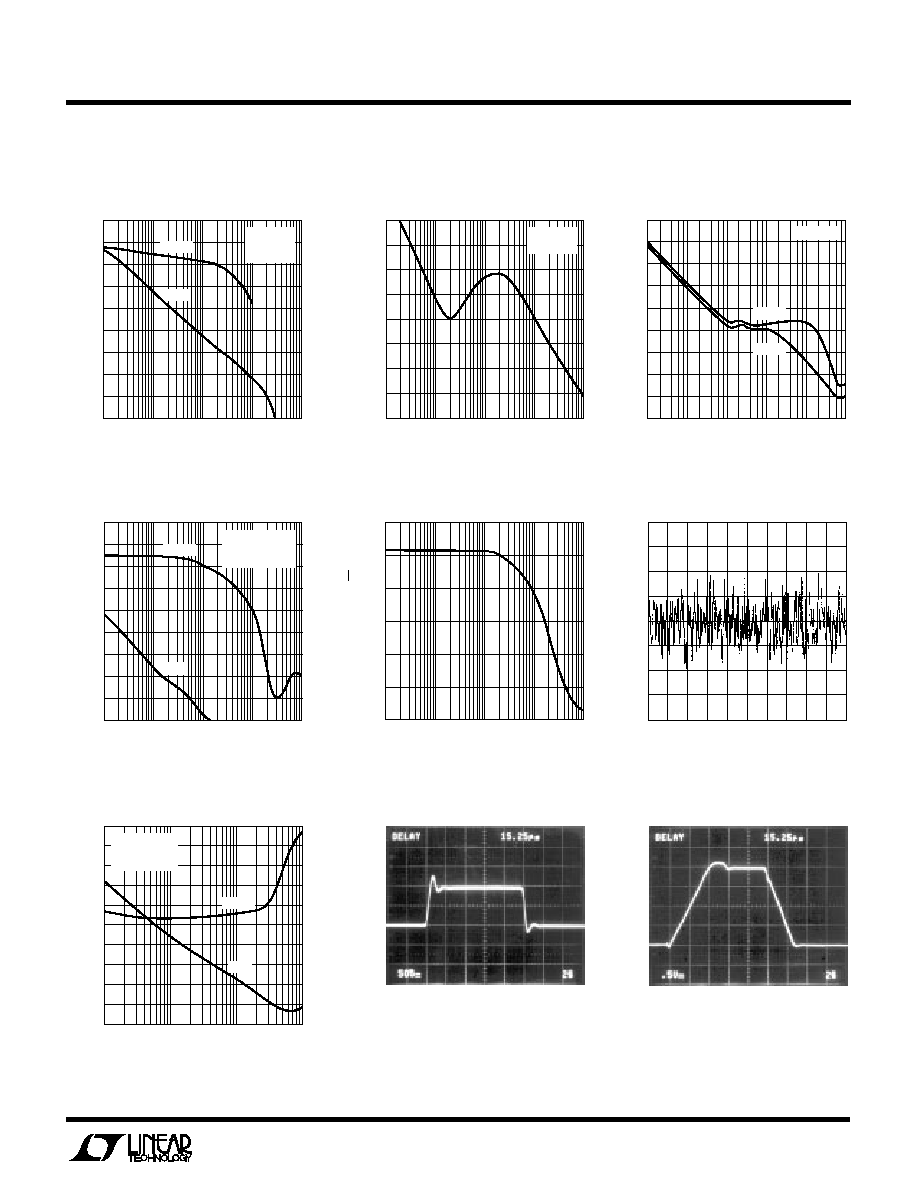
TYPICAL PERFOR
M
A
N
CE CHARACTERISTICS
U
W
POWER SUPPLY VOLTAGE (
±
V)
1
2
COMMON-MODE RANGE LIMIT (V)
3
5
4
6
7
1152 G01
8
6
4
2
0
2
4
6
8
Common-Mode Range vs
Supply Voltage
TOTAL SUPPLY VOLTAGE (V)
0
2
SUPPLY CURRENT (mA)
3.0
2.5
2.0
1.5
1.0
4
6
8
10
1152 G02
12
14
T
A
= 25
°
C
Supply Current vs Supply Voltage
TEMPERATURE (
°
C)
50
25
POWER SUPPLY CURRENT (mA)
2.0
1.9
1.8
1.7
1.6
1.5
1.4
0
25
50
1152 G03
75
100
V
S
= 5V
Output Swing vs Load Resistance
LOAD RESISTANCE (k
)
0.2
OUTPUT SWING (
±
V)
1
5
10
200
1152 G04
0.5
2
20
50 100
6
5
4
3
2
1
0
T
A
= 25
°
C
V
S
= SINGLE 5V
V
S
= SINGLE 3V
V
S
=
±
2.5V
V
S
=
±
1.5V
TOTAL SUPPLY VOLTAGE (V)
2
OUTPUT SHORT-CIRCUIT CURRENT (mA)
40
30
20
10
0
4
6
8
10
1152 G05
12
14
SOURCE
SINK
T
A
= 25
°
C
Output Short-Circuit Current vs
Supply Voltage
TOTAL SUPPLY VOLTAGE (V)
2
OPEN-LOOP OUTPUT RESISTANCE (
)
300
250
200
150
100
4
6
8
10
1152 G06
12
14
T
A
= 25
°
C
Open-Loop Output Resistance vs
Supply Voltage
Charge Pump Voltage vs
Supply Voltage
Charge Pump Voltage vs
Load Current
Input Bias Current vs Temperature
TEMPERATURE (
°
C)
50
INPUT BIAS CURRENT (
±
pA)
1000
100
10
25
25
0
50
75
100
1152 G09
V
S
= 5V
Supply Current vs Temperature
TOTAL SUPPLY VOLTAGE (V)
2
CHARGE PUMP VOLTAGE, V
CP
V
+
(V)
3
2
1
0
4
6
8
10
1152 G07
12
14
T
A
= 25
°
C
LOAD CURRENT (
µ
A)
0
CHARGE PUMP VOLTAGE, V
CP
V
+
(V)
40
60
100
20
80
120 140
160
1152 G08
3
2
1
0
T
A
= 25
°
C
V
S
= 5V
5
LTC1152
TYPICAL PERFOR
M
A
N
CE CHARACTERISTICS
U
W
V
S
=
±
2.5V
A
V
= 1
1152 G16
FREQUENCY (Hz)
POWER SUPPLY REJECTION RATIO (dB)
80
70
60
50
40
30
20
10
0
10
10
1k
10k
1M
1152 G14
100
100k
+PSRR
PSRR
T
A
= 25
°
C
FREQUENCY (kHz)
0.01
VOLTAGE GAIN (dB)
0.1
1
10
1152 G12
60
50
40
30
20
10
0
10
20
30
40
PHASE SHIFT (DEG)
180
160
140
120
100
80
60
40
20
0
20
T
A
= 25
°
C
V
S
=
±
2.5V
C
COMP
= 0.1
µ
F
PHASE
GAIN
Gain and Phase Shift vs
Frequency
Gain and Phase Shift vs
Frequency
FREQUENCY (Hz)
VOLTAGE GAIN (dB)
PHASE SHIFT (DEG)
70
60
50
40
30
20
10
0
10
20
120
100
80
60
40
20
0
1k
100k
1M
10M
1152 G10
10k
T
A
= 25
°
C
V
S
=
±
2.5V
PIN 5 = NC
PHASE
GAIN
Gain and Phase Shift vs
Frequency
Common-Mode Rejection Ratio vs
Frequency
Power Supply Rejection Ratio vs
Frequency
0.1Hz to 10Hz Input Noise
TIME (SEC)
0
(
µ
V)
2
1
0
1
2
8
1152 G18
2
4
6
10
Voltage Noise vs Frequency
FREQUENCY (Hz)
150
125
100
75
50
25
0
1
100
1k
10k
1152 G15
10
VOLTAGE NOISE (nV/
Hz)
Large-Signal Transient Response
V
S
=
±
2.5V
A
V
= 1
1152 G17
Small-Signal Transient Response
FREQUENCY (kHz)
COMMON-MODE REJECTION RATIO (dB)
110
100
90
80
70
60
50
40
30
0.1
10
100
1000
1152 G13
1
T
A
= 25
°
C
V
S
=
±
2.5V
FREQUENCY (Hz)
VOLTAGE GAIN (dB)
PHASE SHIFT (DEG)
1k
100k
1M
10M
1152 G11
10k
T
A
= 25
°
C
V
S
=
±
2.5V
C
COMP
= 1000pF
PHASE
GAIN
70
60
50
40
30
20
10
0
10
20
120
100
80
60
40
20
0
20
40
60