 | –≠–ª–µ–∫—Ç—Ä–æ–Ω–Ω—ã–π –∫–æ–º–ø–æ–Ω–µ–Ω—Ç: LTC1257C | –°–∫–∞—á–∞—Ç—å:  PDF PDF  ZIP ZIP |
1
LTC1257
Complete Single Supply
12-Bit Voltage Output
DAC in SO-8
U
A
O
PPLICATI
TYPICAL
CODE
0
DNL ERROR (LSBs)
0.5
0.0
≠0.5
1024
2048 2560
1257 TA05
512
1536
3072 3584 4098
Differential Nonlinearity
vs Input Code
U
S
A
O
PPLICATI
s
Digital Offset/Gain Adjustment
s
Industrial Process Control
s
Automatic Test Equipment
S
FEATURE
The LTC
Æ
1257 is a complete single supply, 12-bit voltage
output D/A converter (DAC) in an SO-8 package. The
LTC1257 includes an output buffer amplifier, 2.048V
voltage reference and an easy to use three-wire cascadable
serial interface. An external reference can be used to
override the internal reference and extend the output
voltage range to 12V. The power supply current is a low
350
µ
A when operating from a 5V supply, making the
LTC1257 ideal for battery-powered applications. The space-
saving 8-pin SO package and operation with no external
components provide the smallest 12-bit D/A system
available.
D
U
ESCRIPTIO
s
8-Pin SO Package
s
Buffered Voltage Output
s
Built-In 2.048V Reference
s
500
µ
V/LSB with 2.048V Full Scale
s
1/2LSB Max DNL Error
s
Guaranteed 12-Bit Monotonic
s
3-Wire Cascadable Serial Interface
s
Wide Single Supply Range: V
CC
= 4.75V to 15.75V
s
Low Power: I
CC
Typ = 350
µ
A with 5V Supply
, LTC and LT are registered trademarks of Linear Technology Corporation.
µ
P
5V
0.1
µ
F
0.1
µ
F
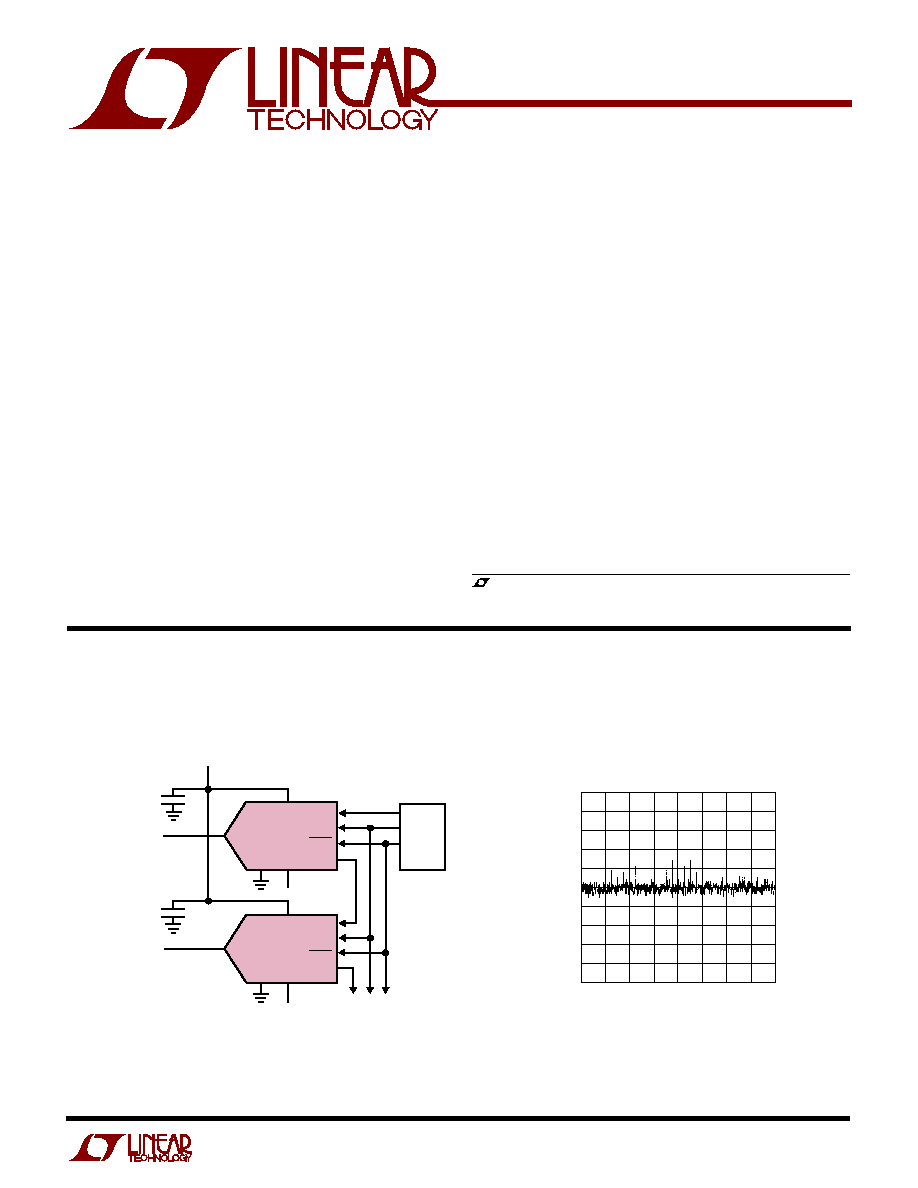
CONTROL OUTPUT 1
CONTROL OUTPUT 2
V
CC
V
REF
GND
V
OUT
D
IN
CLK
LOAD
D
OUT
LTC1257
V
CC
V
REF
GND
V
OUT
D
IN
CLK
LOAD
D
OUT
LTC1257
TO NEXT DAC
1257 TA01
Daisy-Chained Control Outputs
2
LTC1257
V
CC
to GND ............................................ ≠ 0.5V to 16.5V
TTL Input Voltage .......................... ≠ 0.5V to V
CC
+ 0.5V
V
OUT
.............................................. ≠ 0.5V to V
CC
+ 0.5V
REF ................................................ ≠ 0.5V to V
CC
+ 0.5V
Operating Temperature Range
LTC1257C ............................................. 0
∞
C to 70
∞
C
LTC1257I......................................... ≠ 40
∞
C to 85
∞
C
Maximum Junction Temperature
Plastic Package ............................. ≠ 65
∞
C to 125
∞
C
Storage Temperature Range ................ ≠ 65
∞
C to 150
∞
C
Lead Temperature (Soldering, 10 sec)................. 300
∞
C
A
U
G
W
A
W
U
W
A
R
BSOLUTE
XI
TI
S
W
U
U
PACKAGE/ORDER I FOR ATIO
ORDER PART
NUMBER
LTC1257CN8
LTC1257IN8
Consult factory for Military grade parts.
S8 PART MARKING
T
JMAX
= 125
∞
C,
JA
= 100
∞
C/W
T
JMAX
= 125
∞
C,
JA
= 150
∞
C/W
LTC1257CS8
LTC1257IS8
ELECTRICAL C
C
HARA TERISTICS
V
CC
= 4.75V to 15.75V, internal or external reference
(2.475V
V
REF
V
CC
≠ 2.7V), I
OUT
2mA, T
A
= T
MIN
to T
MAX
, unless otherwise noted.
SYMBOL
PARAMETER
CONDITIONS
MIN
TYP
MAX
UNITS
DAC
Resolution
q
12
Bits
DNL
Differential Nonlinearity
Guaranteed Monotonic
q
±
0.5
LSB
INL
Integral Nonlinearity
LTC1257C
q
±
3.5
LSB
LTC1257I
q
±
4.0
LSB
OFF
Offset Error
When Using Internal Reference, LTC1257C
q
±
8
LSB
When Using Internal Reference, LTC1257I
q
±
10
LSB
When Using External Reference, LTC1257C
q
±
4
mV
When Using External Reference, LTC1257I
q
±
5
mV
OFF
TC
Offset Error Tempco
When Using Internal Reference (Note 1)
q
±
0.02
±
0.066
LSB/
∞
C
When Using External Reference (Note 1)
q
±
15
±
30
µ
V/
∞
C
FSE
Full-Scale Error
q
0.5
±
2
LSB
FSE
TC
Full-Scale Error Tempco
(Note 1)
q
±
0.01
±
0.02
LSB/
∞
C
Reference
Reference Output Voltage
I
OUT
= 0, LTC1257C
q
2.028
2.048
2.068
V
I
OUT
= 0, LTC1257I
q
2.018
2.078
V
Reference Output Tempco
I
OUT
= 0
q
±
0.06
LSB/
∞
C
Reference Line Regulation
I
OUT
= 0, LTC1257C
q
±
0.4
LSB/ V
I
OUT
= 0, LTC1257I
q
±
0.7
LSB/V
Reference Load Regulation
0
I
OUT
100
µ
A
q
±
1
LSB
Reference Input Range
V
CC
> V
REF
+ 2.7V
q
2.475
12
V
Reference Input Resistance
q
8
14
18
k
Reference Input Capacitance
(Note 1)
15
pF
Short-Circuit Current
V
OUT
Shorted to GND
q
90
mA
1
2
3
4
8
7
6
5
TOP VIEW
N8 PACKAGE
8-LEAD PDIP
V
CC
V
OUT
REF
GND
CLK
D
IN
LOAD
D
OUT
1
2
3
4
8
7
6
5
TOP VIEW
S8 PACKAGE
8-LEAD PLASTIC SO
V
CC
V
OUT
REF
GND
CLK
D
IN
LOAD
D
OUT
1257
1257I
3
LTC1257
V
CC
= 4.75V to 15.75V, internal or external reference
(2.475V
V
REF
V
CC
≠ 2.7V), I
OUT
2mA, T
A
= T
MIN
to T
MAX
, unless otherwise noted.
ELECTRICAL C
C
HARA TERISTICS
SYMBOL
PARAMETER
CONDITIONS
MIN
TYP
MAX
UNITS
Power Supply
V
CC
Positive Supply Voltage
For Specified Performance
q
4.75
15.75
V
I
CC
Supply Current
4.75V
V
CC
5.25V
q
350
600
µ
A
4.75V
V
CC
15.75V
q
800
1500
µ
A
Op Amp DC Performance
Short-Circuit Current Low
V
OUT
Shorted to GND
q
60
mA
Short-Circuit Current High
V
OUT
Shorted to V
CC
q
60
mA
Output Impedance to GND
Input Code = 0
q
150
400
AC Performance
Voltage Output Slew Rate
5k
in Parallel with 100pF
q
1.0
V/
µ
s
Voltage Output Settling Time
To
±
1/2LSB, 5k
in Parallel with 100pF
q
6
µ
s
Digital Feedthrough
(Notes 1,2)
50
nV/s
Digital I/O
V
IH
Digital Input High Voltage
q
2.4
V
V
IL
Digital Input Low Voltage
q
0.8
V
V
OH
Digital Output High Voltage
I
OUT
= ≠1mA, D
OUT
Only
q
V
CC
≠ 1
V
V
OL
Digital Output Low Voltage
I
OUT
= 1mA, D
OUT
Only
q
0.4
V
I
LEAK
Digital Input Leakage
V
IN
= GND to V
CC
q
±
10
µ
A
C
IN
Digital Input Capacitance
(Note 1)
q
10
pF
Switching (Note 1)
t1
D
IN
Valid to CLK Setup
q
100
ns
t2
D
IN
Valid to CLK Hold
q
25
ns
t3
CLK High Time
q
350
ns
t4
CLK Low Time
q
350
ns
t5
LOAD Pulse Width
q
150
ns
t6
LSB CLK to LOAD
q
0
ns
t7
LOAD High to CLK
q
0
ns
t8
D
OUT
Output Delay
C
LOAD
= 15pF
q
35
150
ns
f
CLK
Maximum Clock Frequency
1.4
MHz
The
q
denotes specifications which apply over the full operating
temperature range.
Note 1: Guaranteed by design; not subject to test.
Note 2: DAC switched from all 1s to all 0s, and all 0s to all 1s code.
4
LTC1257
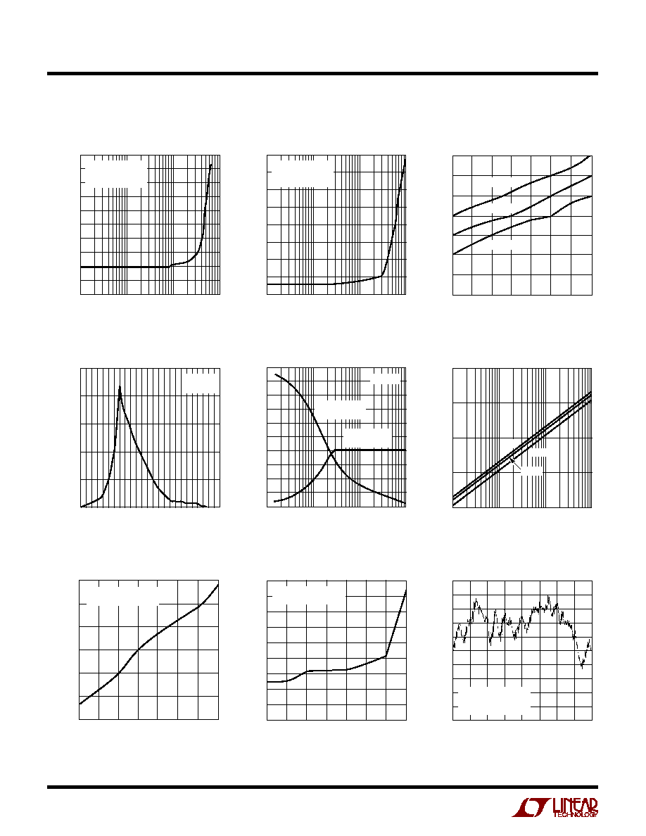
TYPICAL PERFOR
M
A
N
CE CHARACTERISTICS
U
W
TEMPERATURE (∞C)
≠50
0.38
0.37
0.36
0.35
0.34
0.33
0.32
0.31
25
75
1257 G03
≠25
0
50
100
125
SUPPLY CURRENT (mA)
V
CC
= 5.25V
V
CC
= 5V
V
CC
= 4.75V
Supply Current vs Temperature
OUTPUT SINK CURRENT (
µ
A)
1
OUTPUT PULL-DOWN VOLTAGE (mV)
1000
100
10
1
0.1
10
100
1000
1257 G06
HOT
COLD
ROOM
Pull-Down Voltage vs Output Sink
Current Capability
TEMPERATURE (∞C)
≠50
FULL-SCALE VOLTAGE (V)
2.0495
2.0490
2.0485
2.0480
2.0475
2.0470
2.0465
25
75
1257 G07
≠25
0
50
100
125
V
CC
= 5V
INTERNAL REFERENCE
OUTPUT LOAD CURRENT (mA)
0.01
MINIMUM SUPPLY VOLTAGE (V)
0.1
1
10
1257 G01
5.0
4.8
4.6
4.4
4.2
4.0
3.8
3.6
3.4
3.2
3.0
V
REF
= INTERNAL
V
OUT
= FULL SCALE
T
A
= 25∞C
Minimum Supply Voltage
vs Load Current #1
LOGIC VOLTAGE (V)
0
SUPPLY CURRENT (mA)
0.59
0.54
0.49
0.44
0.39
0.34
4
1257 G04
1
2
3
5
V
CC
= 5V
T
A
= 25∞C
Minimum Supply Voltage
vs Load Current #2
OUTPUT LOAD CURRENT (mA)
0.01
MINIMUM SUPPLY VOLTAGE (V)
0.1
1
10
1257 G02
15.0
14.5
14.0
13.5
13.0
12.5
12.0
11.5
11.0
V
REF
= 10V
V
OUT
= FULL SCALE
T
A
= 25∞C
LOAD RESISTANCE (
)
10
OUTPUT VOLTAGE SWING (V)
100
1k
10k
1257 G05
5.0
4.5
4.0
3.5
3.0
2.5
2.0
1.5
1.0
0.5
0
FULL SCALE
R
L
TIED TO GND
ZERO SCALE
R
L
TIED TO V
CC
V
CC
= 5V
Output Swing vs Load Resistance
Supply Current vs
Logic Input Voltage
Full-Scale Voltage vs
Temperature
TEMPERATURE (∞C)
≠50
≠25
25
50
ZERO-SCALE VOLTAGE (mV)
75
100
0.9
0.8
0.7
0.6
0.5
0.4
0.3
0.2
0.1
0
1257 G08
0
125
V
CC
= 5V
INTERNAL REFERENCE
Zero-Scale Voltage vs
Temperature
CODE
0
ERROR (LSB)
2.0
1.6
1.2
0.8
0.4
0
≠0.4
≠0.8
≠1.2
≠1.6
≠2.0
1024
2048 2560
1257 G09
512
1536
3072 3584 4096
V
CC
= 5V
INTERNAL REFERENCE
T
A
= 25∞C
Integral Nonlinearity (INL)
5
LTC1257
TYPICAL PERFOR
M
A
N
CE CHARACTERISTICS
U
W
C
L
(
µ
F)
0.01
REFERENCE COMPENSATION RESISTANCE (
)
70
60
50
40
30
20
10
0
0.1
1
1257 G11
10
100
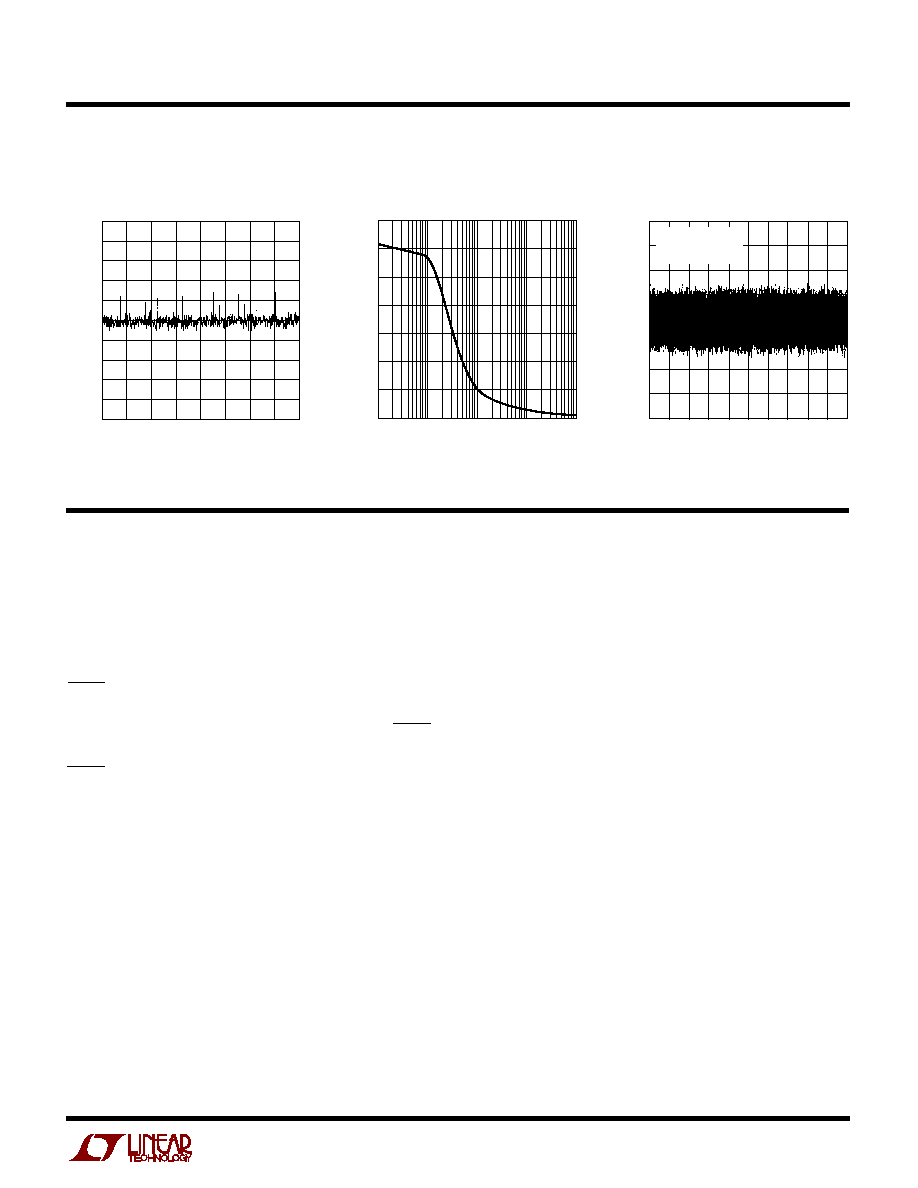
Reference Compensation
Resistance vs C
L
Broadband Noise
PI FU CTIO S
U
U
U
GND (Pin 5): Ground.
REF (Pin 6): The output of the 2.048V reference and the
input to the DAC resistor ladder. An external reference with
voltage from 2.475V to V
CC
≠ 2.7V may be used to override
the internal reference.
V
OUT
(Pin 7): The buffered DAC output is capable of
sourcing 2mA over temperature while pulling within 2.7V
of V
CC
. The output will pull to ground through an internal
200
equivalent resistance.
V
CC
(Pin 8): The positive supply input. 4.75V
V
CC
15.75V. Requires a bypass capacitor to ground.
CLK (Pin 1): The TTL level input for the serial interface
clock.
D
IN
(Pin 2): The TTL level input for the serial interface data.
Data on the D
IN
pin is latched into the shift register on the
rising edge of the serial clock.
LOAD (Pin 3): The TTL level input for the serial interface
load control. Data is loaded from the shift register into the
DAC register, thus updating the DAC output when LOAD is
pulled low. The DAC register is transparent as long as
LOAD is held low.
D
OUT
(Pin 4): The output of the shift register which
becomes valid on the rising edge of the serial clock. The
D
OUT
pin is driven from GND to V
CC
by an internal CMOS
inverter. Multiple LTC1257s may be cascaded by connect-
ing the D
OUT
pin to the D
IN
pin of the next chip.
CODE
0
DNL ERROR (LSBs)
0.5
0.0
≠0.5
1024
2048 2560
1257 TA05
512
1536
3072 3584 4098
Differential Nonlinearity (DNL)
TIME = 5ms/DIV
0.1V/DIV
1257 G12
CODE = FFFH
BW = 3Hz TO 1MHz
GAIN = 1100
◊