Äîêóìåíòàöèÿ è îïèñàíèÿ www.docs.chipfind.ru
1
LTC1261L
TYPICAL APPLICATIO
N
U
DESCRIPTIO
U
APPLICATIO S
U
FEATURES
Switched Capacitor
Regulated Voltage Inverter
s
Regulated Negative Voltage from a
Single Positive Supply
s
REG Pin Indicates Output is in Regulation
s
Adjustable or Fixed Output Voltages
s
Output Regulation:
±
3.5%
s
Supply Current: 650
µ
A Typ
s
Shutdown Mode Drops Supply Current to 5
µ
A
s
Up to 20mA Output Current
s
Requires Only Three or Four External Capacitors
s
Available in MS8 and SO-8 Packages
The LTC
®
1261L is a switched-capacitor voltage inverter
designed to provide a regulated negative voltage from a
single positive supply. The LTC1261L operates from a
single 2.7V to 5.25V supply and provides an adjustable
output voltage from 1.23V to 5V. The LTC1261L-4/
LTC1261L-4.5 needs a single 4.5V to 5.25V supply and
provides a fixed output voltage of 4V to 4.5V respec-
tively. Three external capacitors are required: a 0.1
µ
F
flying capacitor and an input and output bypass capaci-
tors. An optional compensation capacitor at ADJ (COMP)
can be used to reduce the output voltage ripple.
Each version of the LTC1261L will supply up to 20mA
output current with guaranteed output regulation of
±
3.5%.
The LTC1261L includes an open-drain REG output that
pulls low when the output is within 5% of the set value.
Quiescent current is typically 650
µ
A when operating and
5
µ
A in shutdown.
The LTC1261L is available in 8-pin MSOP and SO pack-
ages.
, LTC and LT are registered trademarks of Linear Technology Corporation.
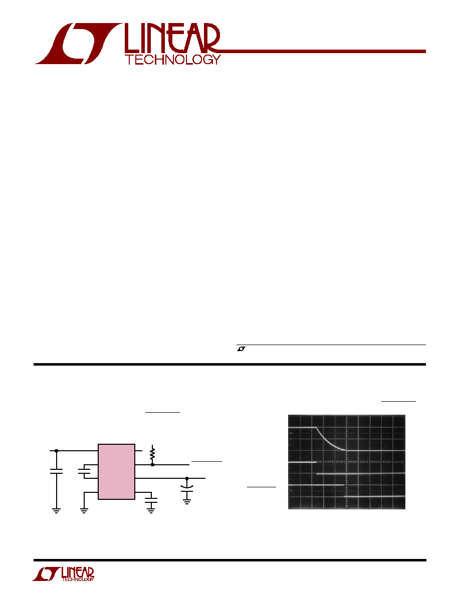
Waveforms for 4V Generator with Power Valid
1261L TAO2
0.1ms/DIV
0V
4V
1
2
3
4
8
7
6
5
LTC1261L-4
SHDN
REG
OUT
COMP
V
CC
C1
+
C1
GND
C2
0.1
µ
F
1261L TA01
C4
3.3
µ
F
V
OUT
= 4V
AT 10mA
POWER VALID
5V
C1
1
µ
F
5V
10k
C3*
100pF
*OPTIONAL
+
4V Generator with Power Valid
s
GaAs FET Bias Generators
s
Negative Supply Generators
s
Battery-Powered Systems
s
Single Supply Applications
5V
0V
5V
0V
POWER VALID
SHDN
OUT
2
LTC1261L
(Note 1)
A
U
G
W
A
W
U
W
A
R
BSOLUTE
XI
TI
S
Supply Voltage (Note 2) ........................................ 5.5V
Output Voltage (Note 3) ........................... 0.3V to 5.3V
Total Voltage, V
CC
to V
OUT
(Note 2) ..................... 10.8V
SHDN Pin .................................. 0.3V to (V
CC
+ 0.3V)
REG Pin ..................................................... 0.3V to 6V
ADJ Pin ........................... (V
OUT
0.3V) to (V
CC
+ 0.3V)
Output Short-Circuit Duration ......................... Indefinite
Commercial Temperature Range ................ 0
°
C to 70
°
C
Extended Commercial Operating
Temperature Range (Note 4) ................. 40
°
C to 85
°
C
Storage Temperature Range ................ 65
°
C to 150
°
C
Lead Temperature (Soldering, 10 sec)................. 300
°
C
W
U
U
PACKAGE/ORDER I FOR ATIO
ORDER PART
NUMBER
MS8 PART MARKING
ORDER PART
NUMBER
S8 PART MARKING
T
JMAX
= 150
°
C,
JA
= 200
°
C/W
1
2
3
4
V
CC
C1
+
C1
GND
8
7
6
5
SHDN
REG
OUT
ADJ (COMP)
TOP VIEW
MS8 PACKAGE
8-LEAD PLASTIC MSOP
LTC1261LCMS8
LTC1261LCMS8-4
LTC1261LCMS8-4.5
1
2
3
4
8
7
6
5
TOP VIEW
SHDN
REG
OUT
ADJ (COMP)
V
CC
C1
+
C1
GND
S8 PACKAGE
8-LEAD PLASTIC SO
T
JMAX
= 150
°
C,
JA
= 135
°
C/W
LTC1261LCS8
LTC1261LCS8-4
LTC1261LCS8-4.5
ELECTRICAL C
C
HARA TERISTICS
LTFM
LTFN
LTFP
1261L
1261L4
261L45
Consult factory for Industrial or Military grade parts or additional fixed voltage parts.
SYMBOL
PARAMETER
CONDITIONS
MIN
TYP
MAX
UNITS
V
CC
Supply Voltage
(LTC1261LCMS8/LTC1261LCS8)
q
2.7
5.25
V
(LTC1261LCMS8-4/LTC1261LCS8-4)
(Note 5)
q
4.35
5.25
V
(LTC1261LCMS8-4.5/LTC1261LCS8-4.5) (Note 5)
q
4.75
5.25
V
V
REF
Reference Voltage
1.23
V
I
CC
Supply Current
V
CC
= 5.25V, No Load, SHDN Floating
q
650
1500
µ
A
V
CC
= 5.25V, No Load, V
SHDN
= V
CC
q
5
20
µ
A
f
OSC
Internal Oscillator Frequency
V
CC
= 5V, V
OUT
= 4V
650
kHz
V
OL
REG Output Low Voltage
I
REG
= 1mA, V
CC
= 5V, V
OUT
= 4V
q
0.1
0.8
V
I
REG
REG Sink Current
V
REG
= 0.8V, V
CC
= 3.3V
q
4
8
mA
V
REG
= 0.8V, V
CC
= 5V
q
5
12
mA
I
ADJ
Adjust Pin Current
V
ADJ
= 1.23V
q
±
0.01
±
1
µ
A
V
IH
SHDN Input High Voltage
V
CC
= 5V
q
2
V
V
IL
SHDN Input Low Voltage
V
CC
= 5V
q
0.8
V
I
IN
SHDN Input Current
V
SHDN
= V
CC
q
2.5
25
µ
A
t
ON
Turn-On Time
V
CC
= 5V, I
OUT
= 10mA, 1.5V
V
OUT
4V (LTC1261L)
q
250
1500
µ
s
V
CC
= 5V, I
OUT
= 5mA, V
OUT
= 4.5V (LTC1261L)
q
250
1500
µ
s
V
CC
= 5V, I
OUT
= 10mA, V
OUT
= 4V (LTC1261L-4)
q
250
1500
µ
s
V
CC
= 5V, I
OUT
= 5mA, V
OUT
= 4.5V (LTC1261L-4.5)
q
250
1500
µ
s
The
q
denotes the specifications which apply over the full operating
temperature range, otherwise specifications are at T
A
= 25
°
C, C1 = 0.1
µ
F, C
OUT
= 3.3
µ
F unless otherwise noted. (Notes 2, 4)
3
LTC1261L
ELECTRICAL C
C
HARA TERISTICS
OUTPUT CURRENT (mA)
0
2.25
OUTPUT VOLTAGE (V)
2.00
1.50
1.25
1.00
20
0
1261L G01
1.75
10
5
25
15
30
0.75
0.50
0.25
T
A
= 25
°
C
V
OUT
= 2V
V
CC
= 2.7V
V
CC
= 3V
SYMBOL
PARAMETER
CONDITIONS
MIN
TYP
MAX
UNITS
V
OUT
Output Regulation (LTC1261L)
2.70V
V
CC
5.25V, 0mA
I
OUT
10mA
q
1.552
1.5
1.448
V
3.25V
V
CC
5.25V, 0mA
I
OUT
20mA
q
1.552
1.5
1.448
V
2.70V
V
CC
5.25V, 0mA
I
OUT
5mA
q
2.070
2.0
1.930
V
2.95V
V
CC
5.25V, 0mA
I
OUT
10mA
q
2.070
2.0
1.930
V
3.50V
V
CC
5.25V, 0mA
I
OUT
20mA
q
2.070
2.0
1.930
V
2.95V
V
CC
5.25V, 0mA
I
OUT
5mA
q
2.587
2.5
2.413
V
3.30V
V
CC
5.25V, 0mA
I
OUT
10mA
q
2.587
2.5
2.413
V
3.85V
V
CC
5.25V, 0mA
I
OUT
20mA
q
2.587
2.5
2.413
V
3.40V
V
CC
5.25V, 0mA
I
OUT
5mA
q
3.105
3.0
2.895
V
3.70V
V
CC
5.25V, 0mA
I
OUT
10mA
q
3.105
3.0
2.895
V
4.25V
V
CC
5.25V, 0mA
I
OUT
20mA
q
3.105
3.0
2.895
V
3.85V
V
CC
5.25V, 0mA
I
OUT
5mA
q
3.622
3.5
3.378
V
4.10V
V
CC
5.25V, 0mA
I
OUT
10mA
q
3.622
3.5
3.378
V
4.60V
V
CC
5.25V, 0mA
I
OUT
20mA
q
3.622
3.5
3.378
V
Output Regulation
4.35V
V
CC
5.25V, 0mA
I
OUT
5mA
q
4.140
4.0
3.860
V
(LTC1261L/LTC1261L-4)
4.60V
V
CC
5.25V, 0mA
I
OUT
10mA
q
4.140
4.0
3.860
V
5.10V
V
CC
5.25V, 0mA
I
OUT
20mA
q
4.140
4.0
3.860
V
Output Regulation
4.75V
V
CC
5.25V, 0mA
I
OUT
5mA
q
4.657
4.5
4.343
V
(LTC1261L/LTC1261L-4.5)
5.05V
V
CC
5.25V, 0mA
I
OUT
10mA
q
4.657
4.5
4.343
V
I
SC
Output Short-Circuit Current
V
OUT
= 0V, V
CC
= 5.25V
q
100
220
mA
Note 4: The LTC1261L is guaranteed to meet specified performance from
0
°
C to 70
°
C and is designed, characterized and expected to meet these
extended commercial temperature limits, but is not tested at 40
°
C and
85
°
C. Guaranteed I grade parts are available, consult factory.
Note 5: The LTC1261L-4 and LTC1261L-4.5 will operate with less than the
minimum V
CC
specified in the electrical characteristics table, but they are
not guaranteed to meet the
±
3.5% V
OUT
specification.
Note 1: The Absolute Maximum Ratings are those values beyond which
the life of a device may be impaired.
Note 2: All currents into device pins are positive; all currents out of device
pins are negative. All voltages are referenced to ground unless otherwise
specified.
Note 3: The output should never be set to exceed V
CC
10.8V.
TYPICAL PERFOR
M
A
N
CE CHARACTERISTICS
U
W
(See Test Circuits)
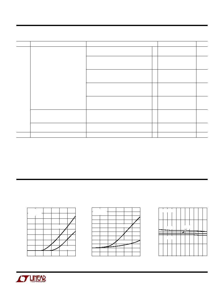
Output Voltage vs Output Current
SUPPLY VOLTAGE (V)
2.5
3.0
3.5
4.0
4.5
5.0
OUTPUT VOLTAGE (V)
2.00
1.95
1261L G03
2.05
2.10
1.90
T
A
= 40
°
C
V
OUT
= 2V
T
A
= 85
°
C
T
A
= 25
°
C
OUTPUT CURRENT (mA)
0
OUTPUT VOLTAGE (V)
3.0
3.1
3.2
3.3
3.4
3.5
3.6
3.7
3.8
3.9
4.0
4.1
4.2
5
10
15
20
1261L G02
25
30
T
A
= 25
°
C
V
OUT
= 4V
V
CC
= 4.5V
V
CC
= 5V
Output Voltage vs Supply Voltage
Output Voltage vs Output Current
The
q
denotes the specifications which apply over the full operating
temperature range, otherwise specifications are at T
A
= 25
°
C, C1 = 0.1
µ
F, C
OUT
= 3.3
µ
F unless otherwise noted. (Notes 2, 4)
4
LTC1261L
TYPICAL PERFOR
M
A
N
CE CHARACTERISTICS
U
W
(See Test Circuits)
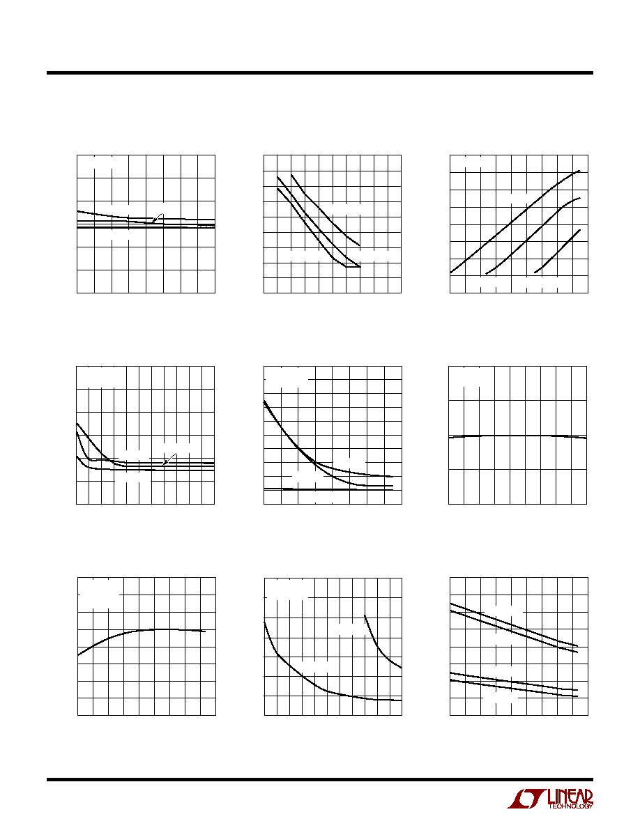
SUPPLY VOLTAGE (V)
4.5
4.15
OUTPUT VOLTAGE (V)
4.10
4.05
4.00
3.95
4.7
4.9
5.1
5.3
1261L G04
3.90
3.85
4.6
4.8
5.0
5.2
V
OUT
= 4V
T
A
= 40
°
C
T
A
= 85
°
C
T
A
= 25
°
C
Output Voltage vs Supply Voltage
SUPPLY VOLTAGE (V)
2.7
MAXIMUM OUTPUT CURRENT (mA)
40
50
60
5.1
1261L G06
30
20
0
3.3
3.9
4.5
3.0
5.4
3.6
4.2
4.8
10
80
70
T
A
= 25
°
C
V
OUT
= 2V
V
OUT
= 3V
V
OUT
= 4V
Maximum Output Current
vs Supply Voltage
Minimum Required V
CC
vs V
OUT
and I
OUT
OUTPUT VOLTAGE (V)
5
2.0
POSITIVE SUPPLY VOLTAGE (V)
2.4
3.2
3.6
4.0
2
1
5.6
1261L G05
2.8
4
3
0
4.4
4.8
5.2
I
OUT
= 5mA
I
OUT
= 10mA
I
OUT
= 20mA
SUPPLY VOLTAGE (V)
0
SUPPLY CURRENT (mA)
1.0
2.0
3.0
0.5
1.5
2.5
3.0
3.5
4.0
4.5
1261L G07
5.0
2.5
T
A
= 40
°
C
T
A
= 85
°
C
T
A
= 25
°
C
V
OUT
= 2V
I
OUT
= 0
Supply Current vs Supply Voltage
Reference Voltage
vs Temperature
Supply Current vs Supply Voltage
SUPPLY VOLTAGE (V)
4.5
0
SUPPLY CURRENT (mA)
0.5
1.5
2.0
2.5
5.0
3.5
4.7
4.9
5.0
1261L G08
1.0
4.0
4.5
3.0
4.6
4.8
5.1
5.2
5.3
T
A
= 85
°
C
V
OUT
= 4.5V
I
OUT
= 0
T
A
= 25
°
C
T
A
= 40
°
C
TEMPERATURE (
°
C)
55
1.21
REFERENCE VOLTAGE (V) 1.22
1.23
1.24
1.25
35 15
5
25
1261L G09
45
65
85 105 125
V
CC
= 5V
ADJ = 0V
Output Short-Circuit Current
vs Temperature
Start-Up Time vs Supply Voltage
Oscillator Frequency
vs Temperature
TEMPERATURE (
°
C)
40
OSCILLATOR FREQUENCY (kHz)
625
650
675
80
1261L G10
600
575
525
10
20
50
25
95
5
35
65
550
725
700
T
A
= 25
°
C
V
OUT
= 4V
V
CC
= 5V
SUPPLY VOLTAGE (V)
2.5
0
START-UP TIME (ms)
0.1
0.3
0.4
0.5
0.7
1261L G11
0.2
0.6
3.0
3.5
4.0
4.5
5.0
V
OUT
= 2V
V
OUT
= 4V
T
A
= 25
°
C
I
OUT
= 10mA
TEMPERATURE (
°
C)
40
SHORT-CIRCUIT CURRENT (mA)
80
100
120
80
1261L G12
60
40
0
10
20
50
25
95
5
35
65
20
160
140
V
CC
= 5.25V
V
CC
= 5V
V
CC
= 3V
V
CC
= 2.7V
5
LTC1261L
PI
N
FU
N
CTIO
N
S
U
U
U
V
CC
(Pin 1): Power Supply. This requires an input voltage
between 2.7V and 5.25V. V
CC
must be bypassed to
ground with at least a 1
µ
F capacitor placed in close
proximity to the chip. See the Applications Information
section for details.
C1
+
(Pin 2): C1 Positive Input. Connect a 0.1
µ
F capacitor
between C1
+
and C1
.
C1
(Pin 3): C1 Negative Input. Connect a 0.1
µ
F capacitor
from C1
+
to C1
.
GND (Pin 4): Ground. Connect to a low impedance
ground. A ground plane will help to minimize regulation
errors.
ADJ (COMP for fixed versions) (Pin 5): Output Adjust/
Compensation Pin. For adjustable parts this pin is used
to set the output voltage. The output voltage is divided
down with an external resistor divider and fed back to this
pin to set the regulated output voltage. Typically the
resistor string should draw
10
µ
A from the output to
minimize errors due to the bias current at the adjust pin.
Fixed output voltage parts have the internal resistor
string connected to this pin inside the package. The pin
can be used to trim the output voltage if desired. It can
also be used as an optional feedback compensation pin to
reduce output ripple on both the adjustable and fixed
output voltage parts. See the Applications Information
section for more information on compensation and out-
put ripple.
OUT (Pin 6): Negative Voltage Output. This pin must be
bypassed to ground with a 1
µ
F or larger capacitor. The
value of the output capacitor and its ESR have a strong
effect on output ripple. See the Applications Information
section for more details.
REG (Pin 7): This is an open-drain output that pulls low
when the output voltage is within 5% of the set value. It
will sink 5mA to ground with a 5V supply. The external
circuitry must provide a pull-up or REG will not swing
high. The voltage at REG may exceed V
CC
and can be
pulled up to 6V above ground without damage.
SHDN (Pin 8): Shutdown. When this pin is at ground the
LTC1261L operates normally. An internal 5
µ
A pull-down
keeps SHDN low if it is left floating. When SHDN is pulled
high, the LTC1261L enters shutdown mode. In shut-
down, the charge pump is disabled, the output collapses
to 0V and the quiescent current drops to 5
µ
A typically.
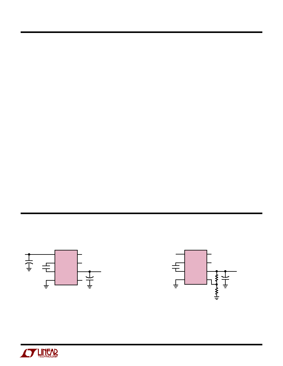
TEST CIRCUITS
Fixed Output
1
2
3
4
8
7
6
5
SHDN
REG
OUT
COMP
V
CC
C1
+
C1
GND
0.1
µ
F
1261L TCO1
3.3
µ
F
V
OUT
= 4V (LTC1261L-4)
V
OUT
= 4.5V (LTC1261L-4.5)
5V
10
µ
F
+
+
LTC1261L-X
Adjustable Output
1
2
3
4
8
7
6
5
SHDN
REG
OUT
ADJ
V
CC
C1
+
C1
GND
V
CC
0.1
µ
F
1261L TCO2
3.3
µ
F
V
OUT
+
LTC1261L