Äîêóìåíòàöèÿ è îïèñàíèÿ www.docs.chipfind.ru
1
LTC1262
12V, 30mA Flash Memory
Programming Supply
S
FEATURE
D
U
ESCRIPTIO
U
A
O
PPLICATI
TYPICAL
s
Regulated 12V
±
5% Output Voltage
s
No Inductors
s
Supply Voltage Range: 4.75V to 5.5V
s
Guaranteed 30mA Output
s
Low Power: I
CC
= 500
µ
A
s
I
CC
in Shutdown: 0.5
µ
A
s
8-Pin PDIP or SO-8 Package
The LTC
®
1262 is a regulated 12V, 30mA output DC/DC
converter. It is designed to provide the 12V
±
5% output
necessary to program byte-wide flash memories. The
output will provide up to 30mA from input voltages as low
as 4.75V without using any inductors. Only four external
capacitors are required to complete an extremely small
surface mountable circuit.
The TTL compatible shutdown pin can be directly con-
nected to a microprocessor and reduces the supply cur-
rent to less than 0.5
µ
A. The LTC1262 offers improved
shutdown current performance and requires fewer exter-
nal components than competing solutions.
The LTC1262 is available in an 8-pin PDIP or SO-8
package.
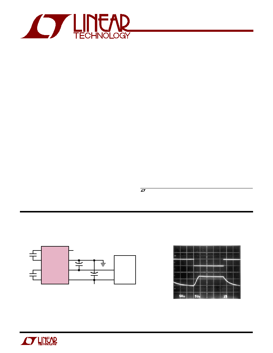
1
2
3
4
8
7
6
5
0.22
µ
F
4.7
µ
F
FROM MPU
4.7
µ
F
V
CC
VPP
LTC1262 · TA01
V
CC
4.75V TO 5.5V
FLASH
MEMORY
0.22
µ
F
C1
C1
+
C2
C2
+
SHDN
GND
V
OUT
V
CC
LTC1262
+
+
U
S
A
O
PPLICATI
s
12V Flash Memory Programming Supplies
s
Compact 12V Op Amp Supplies
s
Battery-Powered Systems
5V
0V
SHDN
5V/DIV
5V
0V
12V
V
OUT
5V/DIV
1ms/DIV
1262 TA01a
In/Out of Shutdown
, LTC and LT are registered trademarks of Linear Technology Corporation.
2
LTC1262
A
U
G
W
A
W
U
W
A
R
BSOLUTE
XI
TI
S
W
U
U
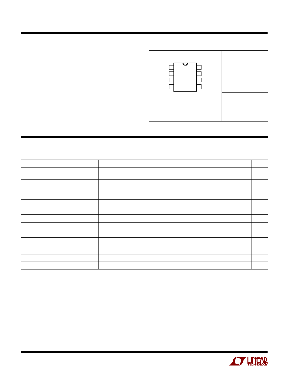
PACKAGE/ORDER I FOR ATIO
(Note 1)
Supply Voltage (V
CC
) ................................................ 6V
Input Voltage (SHDN) ................... 0.3V to V
CC
+ 0.3V
Output Current (I
OUT
) ........................................... 50mA
Operating Temperature Range
LTC1262C................................................ 0
°
C to 70
°
C
LTC1262I ........................................... 40
°
C to 85
°
C
Storage Temperature Range ................ 65
°
C to 150
°
C
Lead Temperature (Soldering, 10 sec)................. 300
°
C
ELECTRICAL CHARACTERISTICS
Consult factory for Military grade parts.
1
2
3
4
8
7
6
5
TOP VIEW
C1
C1
+
C2
C2
+
SHDN
GND
V
OUT
V
CC
N8 PACKAGE
8-LEAD PDIP
S8 PACKAGE
8-LEAD PLASTIC SO
T
JMAX
= 150
°
C,
JA
= 100
°
C/W (N8)
T
JMAX
= 150
°
C,
JA
= 150
°
C/W (S8)
V
CC
= 4.75V to 5.5V, T
A
= 40
°
C to 85
°
C, (Notes 2, 3), unless otherwise noted.
SYMBOL
PARAMETER
CONDITIONS
MIN
TYP
MAX
UNITS
V
OUT
Output Voltage
0mA
I
OUT
30mA, V
SHDN
= 0V, 0
°
C
T
A
70
°
C
q
11.4
12.6
V
0mA
I
OUT
30mA, V
SHDN
= 0V, 40
°
C
T
A
85
°
C
q
11.2
12.6
V
I
CC
Supply Current
No Load, V
SHDN
= 0V, 0
°
C
T
A
70
°
C
q
0.5
1.0
mA
No Load, V
SHDN
= 0V, 40
°
C
T
A
85
°
C
q
0.5
1.3
mA
I
SHDN
Shutdown Supply Current
No Load, V
SHDN
= V
CC
q
0.5
10
µ
A
f
OSC
Oscillator Frequency
V
CC
= 5V, I
OUT
= 30mA
q
300
kHz
Power Efficiency
V
CC
= 5V, I
OUT
= 30mA
q
74
%
R
SW
V
CC
to V
OUT
Switch Impedance
V
CC
= V
SHDN
= 5V, I
OUT
= 0mA
q
0.18
2
k
V
IH
SHDN Input High Voltage
q
2.4
V
V
IL
SHDN Input Low Voltage
q
0.8
V
SHDN Input Current
V
CC
= 5V, V
SHDN
= 0V, 0
°
C
T
A
70
°
C
q
20
10
5
µ
A
V
CC
= 5V, V
SHDN
= 0V, 40
°
C
T
A
85
°
C
q
35
10
5
µ
A
V
CC
= 5V, V
SHDN
= 5V
q
0.06
10
µ
A
t
ON
Turn-On Time
C1 = C2 = 0.22
µ
F, C
IN
= C
OUT
= 4.7
µ
F, (Figures 1, 2)
500
µ
s
t
OFF
Turn-Off Time
C1 = C2 = 0.22
µ
F, C
IN
= C
OUT
= 4.7
µ
F, (Figures 1, 2)
3.3
ms
Note 2: All currents into device pins are positive; all currents out of device
pins are negative. All voltages are referenced to ground unless otherwise
specified.
Note 3: All typicals are given at V
CC
= 5V, T
A
= 25
°
C.
The
q
denotes specifications which apply over the full operating
temperature range.
Note 1: Absolute maximum ratings are those values beyond which the life
of the device may be impaired.
ORDER PART
NUMBER
LTC1262CN8
LTC1262CS8
LTC1262IS8
S8 PART MARKING
1262
1262I
3
LTC1262
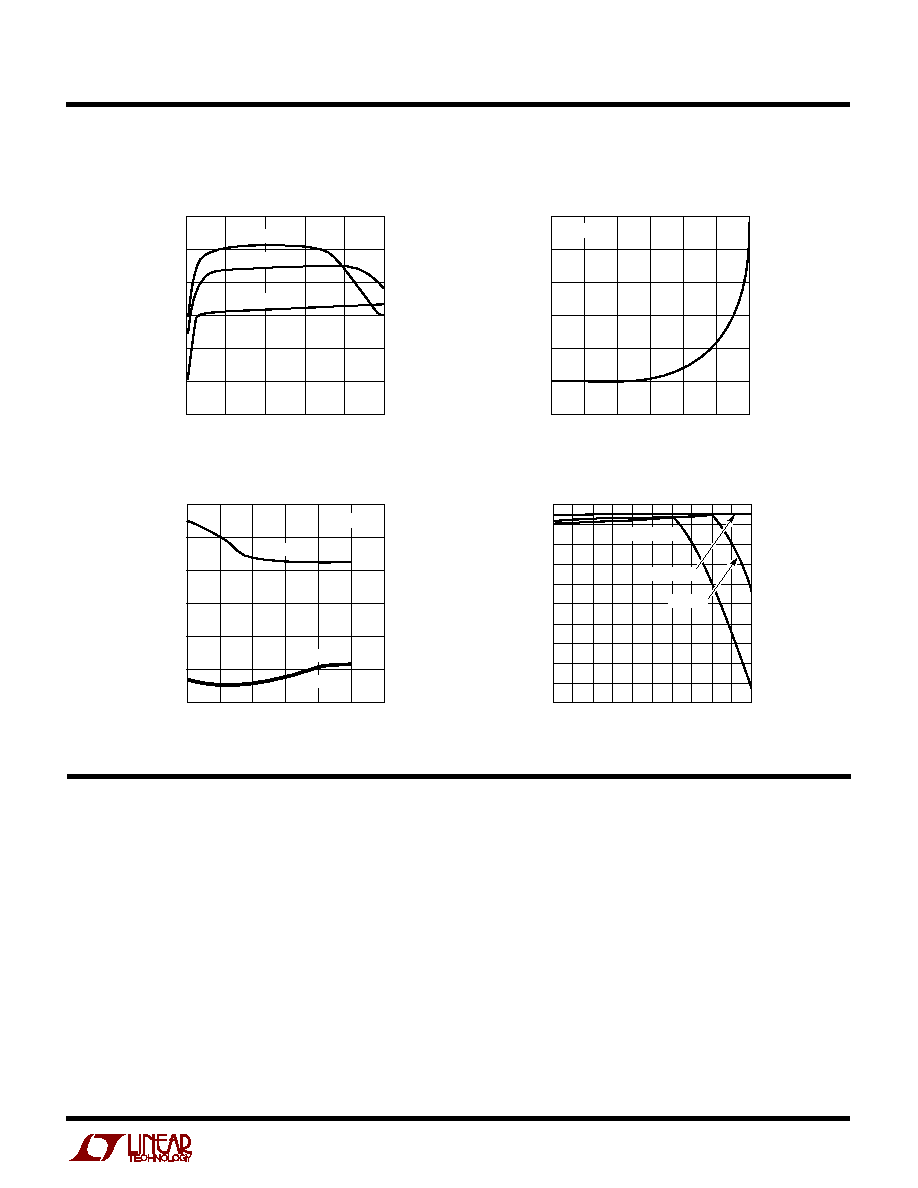
TYPICAL PERFOR
M
A
N
CE CHARACTERISTICS
U
W
PI FU CTIO S
U
U
U
V
OUT
(Pin 6): 12V Output. Connect a 4.7
µ
F bypass capaci-
tor C
OUT
to ground. When in the shutdown mode V
OUT
=
V
CC
.
GND (Pin 7): Ground.
SHDN (Pin 8): Logic Level Shutdown Pin. Application of a
logic low at SHDN pin will place the regulator in normal
operation. With no external connection, or with SHDN tied
to V
CC
, the device will be put into shutdown mode. Connect
to GND for normal operation. In shutdown mode the
charge pump is turned off and V
OUT
= V
CC
.
Efficiency vs Output Current
Shutdown Supply Current
vs Temperature
Output Voltage vs Output Current
C1
(Pin 1): C1 Negative Input. Connect a 0.22
µ
F capaci-
tor C1 between C1
+
and C1
.
C1
+
(Pin 2): C1 Positive Input. Connect a 0.22
µ
F capaci-
tor C1 between C1
+
and C1
.
C2
(Pin 3): C2 Negative Input. Connect a 0.22
µ
F capaci-
tor C2 between C2
+
and C2
.
C2
+
(Pin 4): C2 Positive Input. Connect a 0.22
µ
F capaci-
tor C2 between C2
+
and C2
.
V
CC
(Pin 5): Positive Supply Input Where 4.75V
V
CC
5.5V. Connect a 4.7
µ
F bypass capacitor C
IN
to ground.
Supply Current vs Supply Voltage
SUPPLY VOLTAGE (V)
4.5
480
SUPPLY CURRENT (
µ
A)
500
520
540
560
600
4.75
5.0
5.25
5.5
LTC1262 G03
5.75
6.0
580
T
A
= 70
°
C
I
OUT
= 0
T
A
= 25
°
C
T
A
= 0
°
C
OUTPUT CURRENT (mA)
0
55
EFFICIENCY (%)
60
65
70
75
85
10
20
30
40
LTC1262 G01
50
80
V
CC
= 4.75V
V
CC
= 5V
V
CC
= 5.5V
TEMPERATURE (
°
C)
50
0
SHUTDOWN SUPPLY CURRENT (
µ
A)
0.6
1.2
1.8
2.4
3.6
25
0
25
50
LTC1262 G02
75
100
3.0
V
CC
= 5V
OUTPUT CURRENT (mA)
0
5
10 15 20 25 30 35 40 45 50
OUTPUT VOLTAGE (V)
12.2
12.0
11.8
11.6
11.4
11.2
11.0
10.8
10.6
10.4
10.2
1262 G04
V
CC
= 4.75V
V
CC
= 5.5V
V
CC
= 5V
4
LTC1262
BLOCK DIAGRA
M
W
TI I G DIAGRA S
W
W
U
Figure 2. LTC1262 Timing Circuit
+
S3B
S3D
S3A
S4A
S4B
S1 AND S2 SHOWN WITH SHDN PIN LOW.
S3A, S3B, S3C, S3D, S4A AND S4B SHOWN WITH OSCILLATOR OUTPUT LOW AND V
DIV
< V
BGAP
V
HYST
.
COMPARATOR HYSTERISIS IS
±
V
HYST
.
C1
C1
+
C1
C2
C2
+
C2
CHARGE
PUMP
S3C
D2
D1
V
BGAP
S1
LTC1262 · BD
S2
R3
R1
R2
V
OUT
V
CC
SHDN
GND
C
OUT
BANDGAP
REFERENCE
OSCILLATOR
C
IN
V
DIV
+
+
Figure 1. LTC1262 Timing Diagram
1
2
3
4
8
7
6
5
C1
0.22
µ
F
C2
0.22
µ
F
C
OUT
4.7
µ
F
V
SHUTDOWN
V
OUT
LTC1262 · F02
V
CC
4.75V TO 5V
C
IN
4.7
µ
F
C1
C1
+
C2
C2
+
SHDN
GND
V
OUT
V
CC
LTC1262
+
+
1.4V
5.1V
1.4V
V
SHDN
V
OUT
V
CC
V
CC
V
OUT
11.4V
0V
LTC1262 · F01
t
OFF
t
ON
5
LTC1262
APPLICATIO
N
S I
N
FOR
M
ATIO
N
W
U
U
U
Operation
The LTC1262 uses a charge pump tripler to generate 12V
from a V
CC
of 5V. The charge pump operates when clocked
by a 300kHz oscillator. When the oscillator output is low,
C1 and C2 are connected between V
CC
and GND, charging
them to V
CC
. When the oscillator output goes high, C1 and
C2 are stacked in series with the bottom plate of C1 pulled
to V
CC
. The top plate of C2 is switched to charge C
OUT
and
V
OUT
rises. V
OUT
is regulated to within 5% of 12V by an
oscillator pulse gating scheme. A resistor divider senses
V
OUT
. When the output of the divider (V
DIV
) is less than the
output of a bandgap (V
BGAP
) by the hysteresis voltage
(V
HYST
) of the comparator, oscillator pulses are applied to
the charge pump to raise V
OUT
. When V
DIV
is above V
BGAP
by V
HYST
, the oscillator pulses are prevented from clock-
ing the charge pump. V
OUT
drops until V
DIV
is below V
BGAP
by V
HYST
again. The gates of all internal switches are
driven between V
OUT
and GND. An internal diode ensures
that the LTC1262 will start up under load by charging C
OUT
to one diode drop below V
CC
.
To reduce supply current the LTC1262 may be put into
shutdown mode by floating the SHDN pin or taking it to
V
CC
. In this mode the bandgap, comparator, oscillator and
resistor divider are switched off to reduce supply current
to typically 0.5
µ
A. At the same time an internal switch
shorts V
OUT
to V
CC
; V
OUT
takes 3.3ms to reach 5.1V (see
t
OFF
in Figure 1). When the SHDN pin is low, the LTC1262
exits shutdown and the charge pump operates to raise
V
OUT
to 12V. V
OUT
takes 500
µ
s to reach the lower regula-
tion limit of 11.4V (see t
ON
in Figure 1).
Choice of Capacitors
The LTC1262 is tested with the capacitors shown in
Figure 2. C1 and C2 are 0.22
µ
F ceramic capacitors and
C
IN
and C
OUT
are 4.7
µ
F tantalum capacitors. Refer to
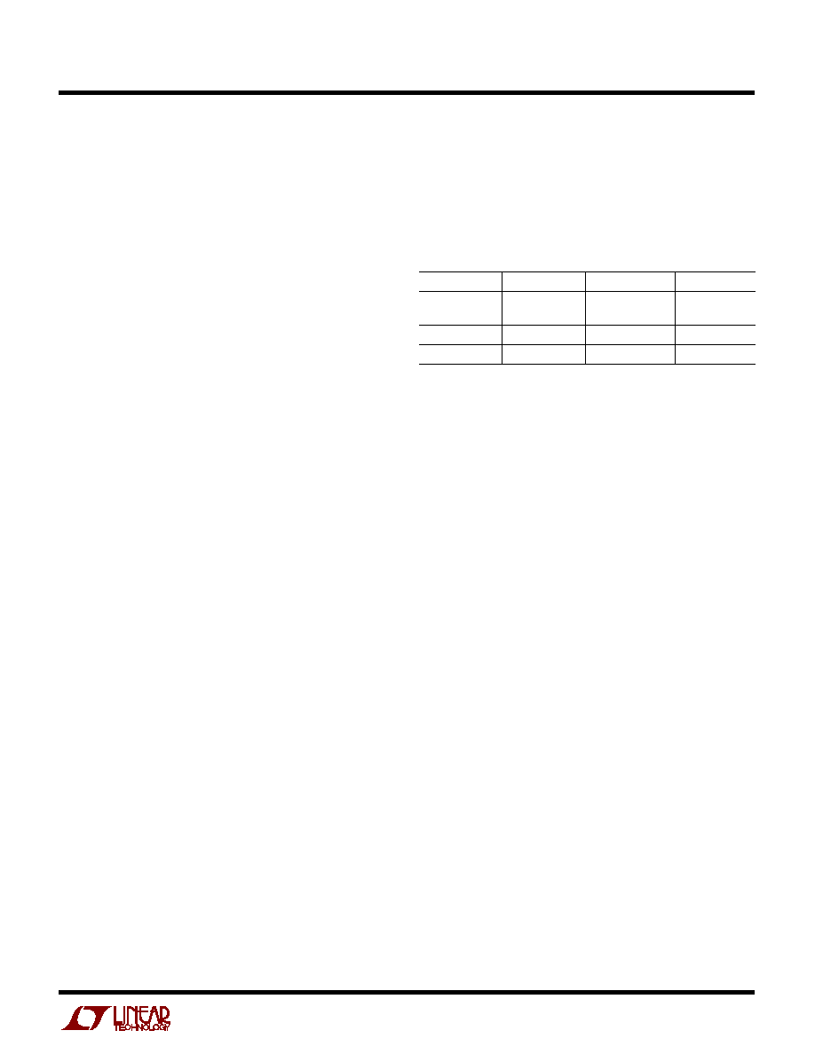
Table 1 if other choices are desired.
Table 1. Recommended Capacitor Types and Values
CAPACITOR
CERAMIC
TANTALUM
ALUMINUM
C1, C2
0.22
µ
F to 1
µ
F
Not
Not
Recommended
Recommended
C
OUT
2
µ
F (Min)
4.7
µ
F (Min)
10
µ
F (Min)
C
IN
1
µ
F (Min)
4.7
µ
F (Min)
10
µ
F (Min)
C1 and C2 should be ceramic capacitors with values in the
range of 0.22
µ
F to 1
µ
F. Higher values provide better load
regulation. Tantalum capacitors are not recommended as
the higher ESR of these capacitors degrades performance
when the load current is above 25mA with V
CC
= 4.75V.
C
IN
and C
OUT
can be ceramic, tantalum or electrolytic
capacitors. The ESR of C
OUT
introduces steps in the V
OUT
waveform whenever the charge pump charges C
OUT
. This
tends to increase V
OUT
ripple. Ceramic or tantalum capaci-
tors are recommended for C
OUT
if minimum ripple is
desired. The LTC1262 does not require a 0.1
µ
F capacitor
between V
CC
and V
OUT
for stability.
Maximum Load Current
The LTC1262 will source up to 50mA continuously without
any damage to itself. Do not short the V
OUT
pin to ground.
If the V
OUT
pin is shorted to ground, irreversible damage
to the device will result.