 | ÐлекÑÑоннÑй компоненÑ: LTC1267C | СкаÑаÑÑ:  PDF PDF  ZIP ZIP |
1267f.pm65
1
LTC1267
LTC1267-ADJ/LTC1267-ADJ5
Dual High Efficiency
Synchronous Step-Down
Switching Regulators
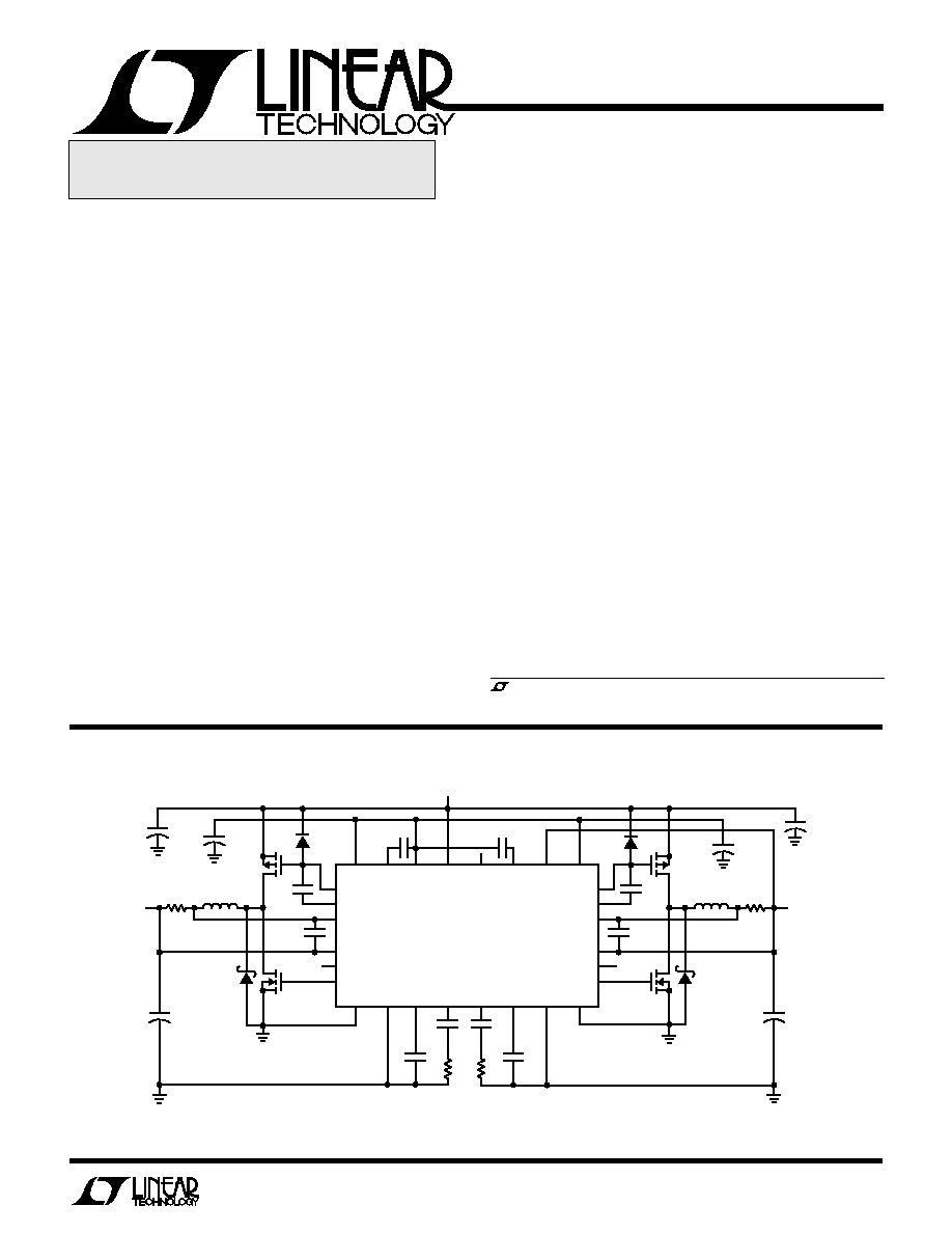
Figure 1. High Efficiency Dual 3.3V, 5V
S
FEATURE
D
U
ESCRIPTIO
The LTC
®
1267 series are dual synchronous step-down
switching regulator controllers featuring automatic Burst
Mode
TM
operation to maintain high efficiencies at low
output currents. The LTC1267 is composed of two sepa-
rate regulator blocks, each driving a pair of external comple-
mentary power MOSFETs at switching frequencies up to
400kHz. The LTC1267 uses a constant off-time current-
mode architecture to provide constant ripple current in the
inductor and provide excellent line and load transient
response.
A separate pin and on-board switch allow the MOSFET
driver power to be derived from the regulated output
voltage, providing significant efficiency improvement when
operating at high input voltage. The output current level is
user-programmable via an external current sense resistor.
The LTC1267 series is ideal for applications requiring dual
output voltages with high conversion efficiencies over a
wide load current range in a small amount of board space.
s
Dual Outputs: 3.3V and 5V, Two Adjustables or
Adjustable and 5V
s
Wide V
IN
Range: 4V to 40V
s
Ultra-High Efficiency: Up to 95%
s
Low Supply Current in Shutdown: 20
µ
A
s
Current Mode Operation for Excellent Line and Load
Transient Response
s
High Efficiency Maintained Over a Wide Output
Current Range
s
Independent Micropower Shutdown
s
Very Low Dropout Operation: 100% Duty Cycle
s
Synchronous FET Switching for High Efficiency
s
Available in Standard 28-Pin SSOP
s
Notebook and Palmtop Computers
s
Battery-Operated Digital Devices
s
Portable Instruments
s
DC Power Distribution Systems
U
S
A
O
PPLICATI
, LTC and LT are registered trademarks of Linear Technology Corporation.
Burst Mode
is a trademark of Linear Technology Corporation.
U
A
O
PPLICATI
TYPICAL
1000pF
+
+
+
1000pF
PGATE 3
PDRIVE 3
SENSE
+
3
SENSE
3
SENSE
5
SHDN3
PDRIVE 5
SHDN5
NGATE 3
PGND3 SGND3 C
T3
I
TH3
I
TH5
C
T5
SGND5 PGND5
NGATE 5
SENSE
+
5
PGATE 5
V
CC3
V
CC
V
IN
CAP3
CAP5
MSHDN
V
CC5
EXT V
CC
LTC1267
C
T5
270pF
7
11
9
10
15
16
20
22
R
C5
1k
C
C3
3300pF
C
C5
3300pF
C
T3
270pF
R
C3
1k
1
3
0.15
µ
F
0.15
µ
F
8
1N4148
26
27
2
21
28
25
24
18
17
19
23
4
5
14
13
12
6
V
OUT5
5V
2A
C
OUT5
220
µ
F
10V
×
2
R
SENSE5
0.05
P-CH
Si9435DY
L5
33
µ
H
D5
MBRS140T3
N-CH
Si9410DY
C
IN5
100
µ
F
50V
+
3.3
µ
F
0.1
µ
F
0.1
µ
F
C
IN3
100
µ
F
50V
P-CH
Si9435DY
N-CH
Si9410DY
D3
MBRS140T3
C
OUT3
220
µ
F
10V
×
2
L3
20
µ
H
R
SENSE3
0.05
V
OUT3
3.3V
2A
V
IN
5.4V to 25V
R
SENSE3
: KRL SL-1R050J
L3: COILTRONICS CTX20-4
R
SENSE5
: KRL SL-1R050J
L5: COILTRONICS CTX33-4
SHDN3, SHDN5, MSHDN
0V = NORMAL, >2V = SHDN
LTC1267 · F01
+
3.3
µ
F
+
1N4148
NOT RECOMMENDED FOR NEW DESIGNS
Contact Linear Technology for Potential Replacement
2
LTC1267
LTC1267-ADJ/LTC1267-ADJ5
A
U
G
W
A
W
U
W
A
R
BSOLUTE
XI
TI
S
Input Supply Voltage (Pin 2) .................... 0.3V to 40V
V
CC
Output Current (Pin 1) .................................. 50mA
EXT V
CC
Input Voltage (Pin 28) .............................. 10V
Continuous Output Current (Pins 5, 6, 23, 24) .... 50mA
Sense Voltages
LTC1267 (Pins 13, 14, 17, 18) ............. V
CC
to 0.3V
LTC1267-ADJ (Pins 12, 13, 17, 18) ..... V
CC
to 0.3V
LTC1267-ADJ5 (Pins 12, 13, 17, 18) ... V
CC
to 0.3V
Shutdown Voltages
LTC1267 (Pins 12, 19, 27) ................................... 7V
LTC1267-ADJ (Pins 11, 27) ................................. 7V
LTC1267-ADJ5 (Pins 11, 19, 27) ......................... 7V
Operating Ambient Temperature Range ...... 0
°
C to 70
°
C
Extended Commercial
Temperature Range ........................... 40
°
C to 85
°
C
Junction Temperature (Note 1) ............................ 125
°
C
Storage Temperature Range ................ 65
°
C to 150
°
C
Lead Temperature (Soldering, 10 sec)................. 300
°
C
W
U
U
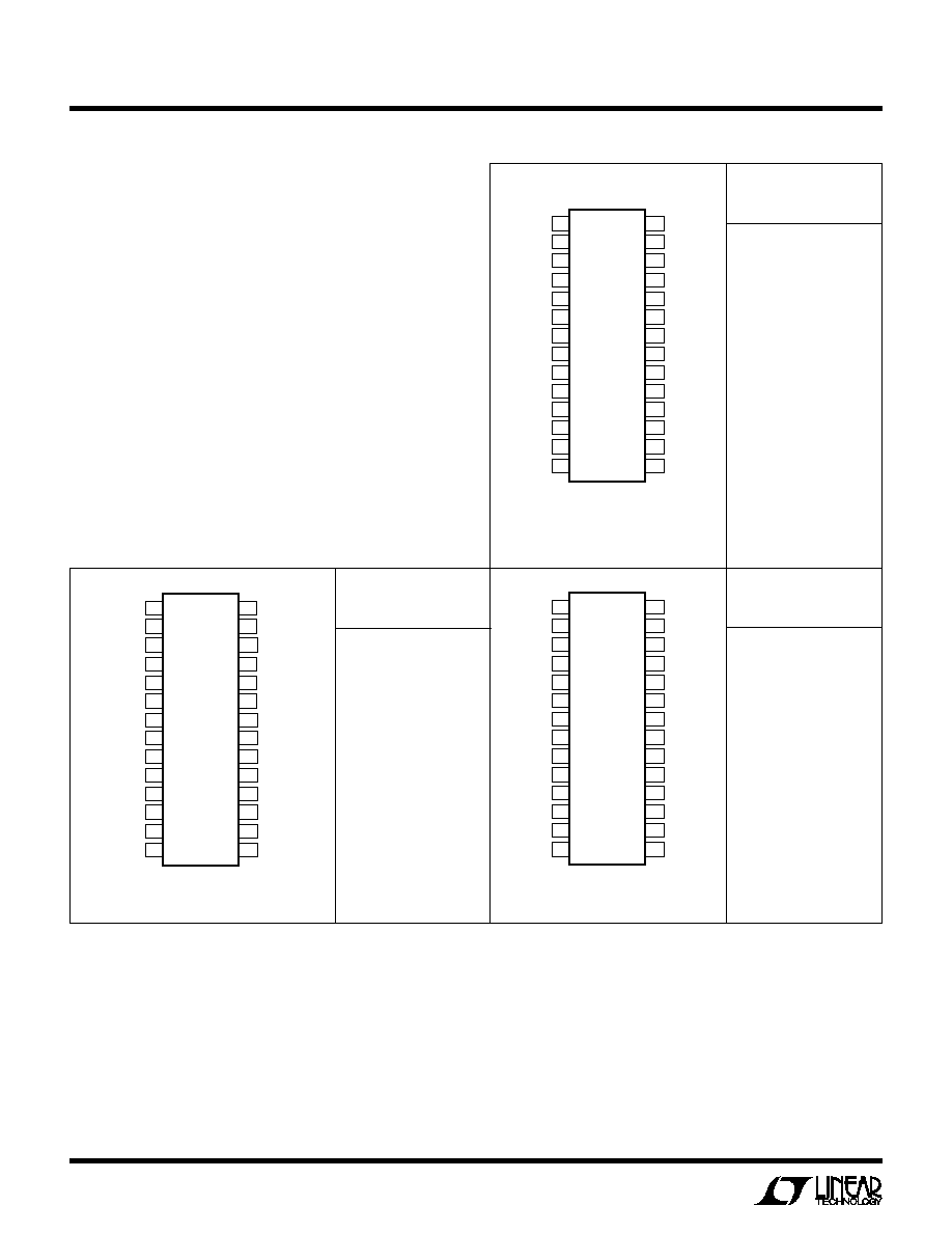
PACKAGE/ORDER I FOR ATIO
ORDER PART
NUMBER
LTC1267CG
ORDER PART
NUMBER
LTC1267CG-ADJ5
ORDER PART
NUMBER
LTC1267CG-ADJ
Consult factory for Industrial and Military grade parts.
The LTC1267 demo circuit board is now available. Consult factory.
1
2
3
4
5
6
7
8
9
10
11
12
13
14
V
CC
V
IN
CAP3
PGATE 3
PDRIVE 3
NGATE 3
PGND3
V
CC3
C
T3
I
TH3
SGND3
SHDN3
SENSE
3
SENSE
+
3
28
27
26
25
24
23
22
21
20
19
18
17
16
15
G PACKAGE
28-LEAD PLASTIC SSOP
T
JMAX
= 125
°
C,
JA
= 95
°
C/W
TOP VIEW
EXT V
CC
MSHDN
CAP5
PGATE 5
PDRIVE 5
NGATE 5
PGND5
V
CC5
SGND5
SHDN5
SENSE
+
5
SENSE
5
C
T5
I
TH5
1
2
3
4
5
6
7
8
9
10
11
12
13
14
V
CC
V
IN
CAP1
PGATE 1
PDRIVE 1
NGATE 1
V
CC1
C
T1
I
TH1
SGND1
SHDN1
SENSE
1
SENSE
+
1
V
FB1
28
27
26
25
24
23
22
21
20
19
18
17
16
15
G PACKAGE
28-LEAD PLASTIC SSOP
T
JMAX
= 125
°
C,
JA
= 95
°
C/W
TOP VIEW
EXT V
CC
MSHDN
CAP5
PGATE 5
PDRIVE 5
NGATE 5
PGND
V
CC5
SGND5
SHDN5
SENSE
+
5
SENSE
5
C
T5
I
TH5
1
2
3
4
5
6
7
8
9
10
11
12
13
14
V
CC
V
IN
CAP1
PGATE 1
PDRIVE 1
NGATE 1
V
CC1
C
T1
I
TH1
SGND1
SHDN1
SENSE
1
SENSE
+
1
V
FB1
28
27
26
25
24
23
22
21
20
19
18
17
16
15
G PACKAGE
28-LEAD PLASTIC SSOP
T
JMAX
= 125
°
C,
JA
= 95
°
C/W
TOP VIEW
EXT V
CC
MSHDN
CAP2
PGATE 2
PDRIVE 2
NGATE 2
PGND
V
CC2
SGND2
V
FB2
SENSE
+
2
SENSE
2
C
T2
I
TH2
3
LTC1267
LTC1267-ADJ/LTC1267-ADJ5
ELECTRICAL C
C
HARA TERISTICS
T
A
= 25
°
C, V
IN
= 12V, V
MSHDN,
V
SHDN1,3,5
= 0V (Note 2), unless otherwise noted.
SYMBOL
PARAMETER
CONDITIONS
MIN
TYP
MAX
UNITS
V
FB1
,
2
Feedback Voltage
LTC1267-ADJ, LTC1267-ADJ5: V
IN
= 9V
q
1.21
1.25
1.29
V
I
FB1
,
2
Feedback Current
LTC1267-ADJ, LTC1267-ADJ5
q
0.2
1
µ
A
V
OUT
Regulated Output Voltage
3.3V Output
LTC1267: V
IN
= 9V, I
LOAD
= 700mA
q
3.23
3.33
3.43
V
5V Output
LTC1267, LTC1267-ADJ5: V
IN
= 9V, I
LOAD
= 700mA
q
4.90
5.05
5.20
V
V
OUT
Output Voltage Line Regulation
V
IN
= 9V to 40V
40
0
40
mV
Output Voltage Load Regulation
Figure 1 Circuit
3.3V Output
5mA < I
LOAD
< 2.0A
q
40
65
mV
5V Output
5mA < I
LOAD
< 2.0A
q
60
100
mV
Burst Mode Output Ripple
I
LOAD
= 0A
50
mV
P-P
V
CC
Internal Regulator Voltage
V
IN
= 12V to 30V, EXT V
CC
= 0V, I
CC
= 10mA
q
4.25
4.5
4.75
V
V
IN
V
CC
V
CC
Dropout Voltage
V
IN
= 4V, EXT V
CC
= Open, I
CC
= 10mA
200
300
mV
I
EXTVCC
EXT V
CC
Pin Current (Note 3)
EXT V
CC
= 5V, Sleep Mode
360
µ
A
I
IN
V
IN
Pin Current (Note 3)
Normal
V
IN
= 12V, EXT V
CC
= 5V
320
µ
A
V
IN
= 40V, EXT V
CC
= 5V
550
µ
A
Shutdown
V
IN
= 12V, V
MSHDN
= 2V
15
µ
A
V
IN
= 40V, V
MSHDN
= 2V
25
µ
A
V
EXTVCC
EXT V
CC
Switch Drop
V
IN
= 12V, EXT V
CC
= 5V, I
SWITCH
= 10mA
200
300
mV
V
CC
V
PGATE
PGate to Source Voltage (Off)
V
IN
= 12V
0.2
0
V
V
IN
V
IN
= 40V
0.2
0
V
V
SENSE
+
1, 2
Current Sense Threshold Voltage
LTC1267-ADJ, LTC1267-ADJ5
V
SENSE
1, 2
V
SENSE
1, 2
= 5.1V, V
FB1, 2
= V
OUT
/4 + 25mV (Forced)
25
mV
V
SENSE
1, 2
= 4.9V, V
FB1, 2
= V
OUT
/4 25mV (Forced)
q
130
155
180
mV
V
SENSE
+
3, 5
Current Sense Threshold Voltage
LTC1267
V
SENSE
3, 5
V
SENSE
3, 5
= V
OUT
+ 100mV (Forced)
25
mV
V
SENSE
3, 5
= V
OUT
100mV (Forced)
q
130
155
180
mV
V
SHDN
Shutdown Threshold
MSHDN
0.8
1.4
2.0
V
SHDN1, 3, 5
0.6
0.8
2.0
V
I
MSHDN
MSHDN Input Current
V
MSHDN
= 5V
12
20
µ
A
I
CT
C
T
Pin Discharge Current
V
OUT
in Regulation
50
70
90
µ
A
V
OUT
= 0V
2
10
µ
A
t
OFF
Off-Time (Note 4)
C
T
= 390pF, I
LOAD
= 700mA, V
IN
= 10V
4
5
6
µ
s
t
r
, t
f
Driver Output Transition Times
C
L
= 3000pF (PDrive and NGate Pins), V
IN
= 6V
100
200
ns
4
LTC1267
LTC1267-ADJ/LTC1267-ADJ5
SYMBOL
PARAMETER
CONDITIONS
MIN
TYP
MAX
UNITS
V
FB1
,
2
Feedback Voltage
LTC1267-ADJ, LTC1267-ADJ5: V
IN
= 9V
1.2
1.25
1.3
V
V
OUT
Regulated Output Voltage
V
IN
= 9V
3.3V Output
I
LOAD
= 700mA
3.17
3.30
3.48
V
5V Output
I
LOAD
= 700mA
4.85
5.05
5.25
V
I
IN
V
IN
Pin Current (Note 3)
Normal
V
IN
= 12V, EXT V
CC
= 5V
320
µ
A
V
IN
= 40V, EXT V
CC
= 5V
550
µ
A
Shutdown
V
IN
= 12V, V
MSHDN
= 2V
15
µ
A
V
IN
= 40V, V
MSHDN
= 2V
25
µ
A
I
EXTVCC
EXT V
CC
Pin Current (Note 3)
EXT V
CC
= 5V, Sleep Mode
360
µ
A
V
CC
Internal Regulator Voltage
V
IN
= 12V to 40V, EXT V
CC
= 0V, I
CC
= 20mA
4.5
V
V
SENSE
+
Current Sense Threshold Voltage
Low Threshold (Forced)
25
mV
V
SENSE
High Threshold (Forced)
130
160
185
mV
V
MSHDN
Shutdown Threshold MSHDN
0.8
1.4
2.0
V
t
OFF
Off-Time (Note 4)
C
T
= 390pF, I
LOAD
= 700mA, V
IN
= 10V
3
5
7
µ
s
ELECTRICAL C
C
HARA TERISTICS
40
°
C
T
A
85
°
C, V
IN
= 12V, V
MSHDN,
V
SHDN1,3,5
= 0V (Notes 2, 5), unless otherwise noted.
The
q
denotes specifications which apply over the full operating
temperature range.
Note 1: T
J
is calculated from the ambient temperature T
A
and power
dissipation P
D
according to the following formula:
LTC1267/LTC1267-ADJ/LTC1267ADJ5: T
J
= T
A
+ (P
D
×
95
°
C/ W)
Note 2: On LTC1267 versions which have MSHDN and SHDN1, 3, 5 pins,
they must be at ground potential for testing.
Note 3: The LTC1267 V
IN
and EXT V
CC
current measurements exclude
MOSFET driver currents. When V
CC
power is derived from the output via
EXT V
CC
, the input current increases by (I
GATECHG
×
Duty Cycle)/Efficiency.
See Typical Performance Characteristics and Applications Information.
Note 4: In applications where R
SENSE
is placed at ground potential, the
off-time increases approximately 40%.
Note 5: The LTC1267/LTC1267-ADJ/LTC1267-ADJ5 are not tested and
quality-assurance sampled at 40
°
C to 85
°
C. These specifications are
guaranteed by design and/or correlation.
Note 6: The logic level power MOSFETs shown in Figure 1 are rated for
V
DS(MAX)
= 30V. For operation at V
IN
> 30V, use standard threshold
MOSFETs with EXT V
CC
powered from a 9V supply. See applications
information.
Note 7: LTC1267-ADJ and LTC1267-ADJ5 are tested at an output of 3.3V
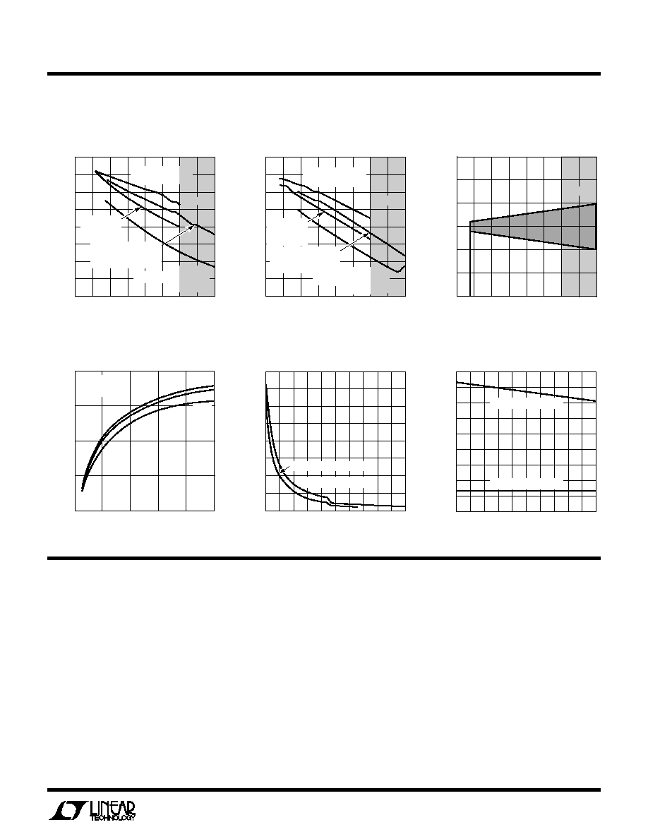
TYPICAL PERFOR
M
A
N
CE CHARACTERISTICS
U
W
LOAD CURRENT (A)
0.01
80
EFFICIENCY (%)
90
100
0.1
1
10
LTC1267 · G01
70
75
85
95
65
60
V
IN
= 10V
V
IN
= 20V
5V Output Efficiency
vs Load Current
LOAD CURRENT
0
60
OUTPUT VOLTAGE (mV)
50
30
20
10
1.0
2.0
2.5
30
LTC1267 · G03
40
0.5
1.5
0
10
20
V
IN
= 10V
V
OUT
= 3.3V
V
IN
= 20V
V
OUT
= 3.3V
V
IN
= 10V
V
OUT
= 5V
V
IN
= 20V
V
OUT
= 5V
Load Regulation
LOAD CURRENT (A)
0.01
80
EFFICIENCY (%)
90
100
0.1
1
10
LTC1267 · G02
70
75
85
95
65
60
V
IN
= 10V
V
IN
= 20V
3.3V Output Efficiency
vs Load Current
5
LTC1267
LTC1267-ADJ/LTC1267-ADJ5
TYPICAL PERFOR
M
A
N
CE CHARACTERISTICS
U
W
5V Output Efficiency
vs Line Voltage
Line Regulation
3.3V Output Efficiency
vs Line Voltage
INPUT VOLTAGE (V)
0
EFFICIENCY (%)
80
85
90
40
LTC1267 · G04
75
70
60
10
20
30
65
100
95
5
15
25
35
LOGIC THRESHOLD
GATE, 1A
STANDARD
THRESHOLD GATE, 1A
V
EXTVCC
= 9V
LOGIC
THRESHOLD
GATE, 0.1A
STANDARD
THRESHOLD GATE, 0.1A
V
EXTVCC
= 9V
NOTE 6
INPUT VOLTAGE (V)
0
EFFICIENCY (%)
80
85
90
40
LTC1267 · G05
75
70
60
10
20
30
65
100
95
5
15
25
35
LOGIC THRESHOLD
GATE, 1A
STANDARD
THRESHOLD GATE, 1A
V
EXTVCC
= 9V
LOGIC
THRESHOLD
GATE, 0.1A
STANDARD
THRESHOLD GATE, 0.1A
V
EXTVCC
= 9V
NOTE 6
INPUT VOLTAGE (V)
0
60
OUTPUT VOLTAGE (mV)
40
20
0
20
10
20
30
40
LT1267 · G06
40
60
5
15
25
35
NOTE 6
Operating Frequency
vs (V
IN
V
OUT
)
Current Sense Threshold Voltage
(V
IN
V
OUT
) VOLTAGE (V)
0
NORMALIZED FREQUENCY (Hz)
1.0
1.5
20
LTC1267 · G07
0.5
0
5
10
15
25
2.0
0
°
C
25
°
C
V
OUT
= 5V
I
LOAD
= 700mA
70
°
C
Off-Time vs Output Voltage
OUTPUT VOLTAGE (V)
0
OFF-TIME (
µ
s)
120
160
4.0
LTC1267 · F08
80
40
100
140
60
20
0
1.0
2.0
3.0
0.5
4.5
1.5
2.5
3.5
5.0
3.3V OUTPUT REGULATOR
5V OUTPUT REGULATOR
TEMPERATURE (
°
C)
0
0
SENSE VOLTAGE (mV)
20
60
80
100
20
180
LTC1267 · G09
40
10
30 40 50 60 70 80 90 100
120
140
160
MINIMUM THRESHOLD
MAXIMUM THRESHOLD
PI FU CTIO S
U
U
U
(Applies to both regulator sections)
V
IN
: Main Supply Input Pin.
EXT V
CC
: External V
CC
Supply for the Regulators. See EXT
V
CC
Pin Connection.
V
CC
: Output of the Internal 4.5V Linear Regulator, EXT V
CC
Switch, and Supply Inputs for Driver and Control Circuits.
The driver and control circuits are powered from the
higher of the 4.5V regulator or EXT V
CC
voltage. Must be
closely decoupled to the power ground.
PGND: Power Ground. Connect to the source of N-channel
MOSFET and the () terminal of C
IN
.
SGND: Small-Signal Ground. Must be routed separately
from other grounds to the () terminal of C
OUT
.
PGATE: Level Shifted Gate Drive for the Top P-channel
MOSFET. The voltage swing at the PGate pin is from V
IN
to
(V
IN
V
CC
).
PDRIVE: High Current Gate Drive for the Top P-channel
MOSFET. The PDrive pin swings from V
CC
to GND.
NGATE: High Current Drive for the Bottom N-channel
MOSFET. The NGate pin swings from GND to V
CC
.