1
LTC1272
12-Bit, 3
µ
s, 250kHz
Sampling A/D Converter
D
U
ESCRIPTIO
s
AD7572 Pinout
s
12-Bit Resolution
s
3
µ
s and 8
µ
s Conversion Times
s
On-Chip Sample-and-Hold
s
Up to 250kHz Sample Rates
s
5V Single Supply Operation
s
No Negative Supply Required
s
On-Chip 25ppm/
∞
C Reference
s
75mW (Typ) Power Consumption
s
24-Pin Narrow DIP and SOL Packages
s
ESD Protected on All Pins
S
FEATURE
s
High Speed Data Acquisition
s
Digital Signal Processing (DSP)
s
Multiplexed Data Acquisition Systems
s
Single Supply Systems
U
S
A
O
PPLICATI
The LTC1272 is a 3
µ
s, 12-bit, successive approximation
sampling A/D converter. It has the same pinout as the
industry standard AD7572 and offers faster conversion
time, on-chip sample-and-hold, and single supply opera-
tion. It uses LTBiCMOS
TM
switched-capacitor technology to
combine a high speed 12-bit ADC with a fast, accurate
sample-and-hold and a precision reference.
The LTC1272 operates with a single 5V supply but can also
accept the 5V/≠15V supplies required by the AD7572 (Pin
23, the negative supply pin of the AD7572, is not connected
on the LTC1272). The LTC1272 has the same 0V to 5V input
range as the AD7572 but, to achieve single supply opera-
tion, it provides a 2.42V reference output instead of the
≠ 5.25V of the AD7572. It plugs in for the AD7572 if the
reference capacitor polarity is reversed and a 1
µ
s sample-
and-hold acquisition time is allowed between conversions.
The output data can be read as a 12-bit word or as two
8-bit bytes. This allows easy interface to both 8-bit and
higher processors. The LTC1272 can be used with a
crystal or an external clock and comes in speed grades of
3
µ
s and 8
µ
s.
FREQUENCY (kHz)
0
≠140
AMPLITUDE (dB)
20
40
60
80
LTC1272 ∑ TA02
≠120
≠100
≠80
≠60
≠40
≠20
0
100
120
S
(N+D)
= 72.1
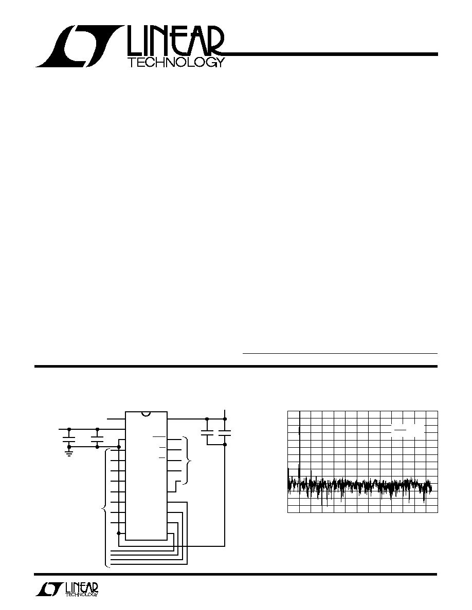
Single 5V Supply, 3
µ
s, 12-Bit Sampling ADC
10 F
µ
IN
REF
D11 (MSB)
D10
D9
D8
D7
CLK IN
CLK OUT
HBEN
RD
CS
BUSY
NC
V
LTC1272
D6
D5
D4
DGND
D3/11
D2/10
D1/9
D0/8
A
V
AGND
DD
P
CONTROL
LINES
µ
µ
0.1 F
5V
8 OR 12-BIT
PARALLEL
BUS
ANALOG INPUT
(0V TO 5V)
10
µ
F
0.1
µ
F
LTC1272 ∑ TA01
+
+
2.42V
V
OUTPUT
REF
U
A
O
PPLICATI
TYPICAL
LTBiCMOS is a trademark of Linear Technology Corporation
1024 Point FFT, f
S
= 250kHz, f
IN
= 10kHz
LTC1272
2
A
U
G
W
A
W
U
W
A
R
BSOLUTE
XI
TI
S
Supply Voltage (V
DD
) ................................................. 6V
Analog Input Voltage (Note 3) ................... ≠ 0.3V to 15V
Digital Input Voltage .................................. ≠ 0.3V to 12V
Digital Output Voltage .................... ≠ 0.3V to V
DD
+ 0.3V
Power Dissipation .............................................. 500mW
Operating Temperature Range
LTC1272-XAC, CC ................................. 0
∞
C to 70
∞
C
Storage Temperature Range ................. ≠ 65
∞
C to 150
∞
C
Lead Temperature (Soldering, 10 sec) .................. 300
∞
C
(Notes 1 and 2)
W
U
U
PACKAGE/ORDER I FOR ATIO
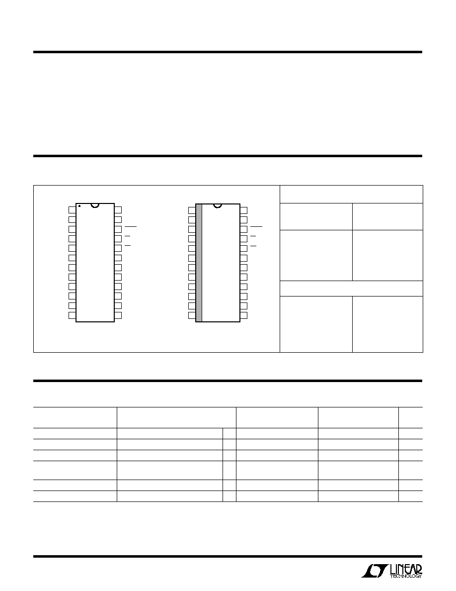
Consult factory for Industrial and Military grade parts.
LTC1272-XA
LTC1272-XC
PARAMETER
CONDITIONS
MIN
TYP
MAX
MIN
TYP
MAX
UNITS
Resolution (No Missing Codes)
q
12
12
Bits
Integral Linearity Error
(Note 5)
q
±
1/2
±
1
LSB
Differential Linearity Error
q
±
1
±
1
LSB
Offset Error
±
3
±
4
LSB
q
±
4
±
6
LSB
Gain Error
±
10
±
15
LSB
Full-Scale Tempco
I
OUT
(Reference) = 0
q
±
5
±
25
±
10
±
45
ppm/
∞
C
C
C
HARA TERISTICS
CO
U
VERTER
With Internal Reference (Note 4)
CONVERSION
CONVERSION
TIME = 3
µ
s
TIME = 8
µ
s
LTC1272-3ACN
LTC1272-8ACN
LTC1272-3CCN
LTC1272-8CCN
S PACKAGE ONLY
LTC1272-3ACS
LTC1272-8ACS
LTC1272-3CCS
LTC1272-8CCS
24
23
22
21
20
19
18
17
8
7
6
5
4
3
2
1
IN
REF
(MSB) D11
D10
D9
D8
D7
CLK IN
CLK OUT
HBEN
RD
CS
BUSY
NC
V
TOP VIEW
16
15
14
13
12
11
10
9
D6
D5
D4
DGND
D3/11
D2/10
D1/9
D0/8
A
V
AGND
DD
S PACKAGE
24-LEAD PLASTIC SOL
T
JMAX
= 110
∞
C,
JA
= 130
∞
C/W
24
23
22
21
20
19
18
17
8
7
6
5
4
3
2
1
IN
REF
(MSB) D11
D10
D9
D8
D7
CLK IN
CLK OUT
HBEN
RD
CS
BUSY
NC
V
TOP VIEW
16
15
14
13
12
11
10
9
D6
D5
D4
DGND
D3/11
D2/10
D1/9
D0/8
A
V
AGND
DD
N PACKAGE
24-LEAD PLASTIC DIP
T
JMAX
= 110
∞
C,
JA
= 100
∞
C/W
ORDER PART NUMBER
3
LTC1272
LTC1272-XA
LTC1272-XC
PARAMETER
CONDITIONS
MIN
TYP
MAX
MIN
TYP
MAX
UNITS
V
REF
Output Voltage (Note 6)
I
OUT
= 0
2.400
2.420
2.440
2.400
2.420
2.440
V
V
REF
Output Tempco
I
OUT
= 0
q
5
25
10
45
ppm/
∞
C
V
REF
Line Regulation
4.75V
V
DD
5.25V, I
OUT
= 0
0.01
0.01
LSB/V
V
REF
Load Regulation (Sourcing Current) 0
I
OUT
1mA
2
2
LSB/mA
LTC1272-XA/C
SYMBOL
PARAMETER
CONDITIONS
MIN
TYP
MAX
UNITS
V
IH
High Level Input Voltage CS, RD, HBEN, CLK IN
V
DD
= 5.25V
q
2.4
V
V
IL
Low Level Input Voltage CS, RD, HBEN, CLK IN
V
DD
= 4.75V
q
0.8
V
I
IN
Input Current CS, RD, HBEN
V
IN
= 0V to V
DD
q
±
10
µ
A
Input Current CLK IN
V
IN
= 0V to V
DD
q
±
20
µ
A
V
OH
High Level Output Voltage All Logic Outputs
V
DD
= 4.75V I
OUT
= ≠ 10
µ
A
4.7
V
I
OUT
= ≠ 200
µ
A
q
4.0
V
V
OL
Low Level Output Voltage All Logic Outputs
V
DD
= 4.75V, I
OUT
= 1.6mA
q
0.4
V
I
OZ
High-Z Output Leakage D11-D0/8
V
OUT
= 0V to V
DD
q
±
10
µ
A
C
OZ
High-Z Output Capacitance (Note 7)
q
15
pF
I
SOURCE
Output Source Current
V
OUT
= 0V
≠ 10
mA
I
SINK
Output Sink Current
V
OUT
= V
DD
10
mA
I
DD
Positive Supply Current
CS = RD = V
DD
, A
IN
= 5V
q
15
30
mA
P
D
Power Dissipation
75
mW
ACCURACY
IC
DY
U
W
A
LTC1272-XA/C
SYMBOL
PARAMETER
CONDITIONS
MIN
TYP
MAX
UNITS
S/(N + D)
Signal-to-Noise Plus Distortion Ratio
10kHz Input Signal
72
dB
THD
Total Harmonic Distortion (Up to 5th Harmonic)
10kHz Input Signal
≠ 82
dB
Peak Harmonic or Spurious Noise
10kHz Input Signal
≠ 82
dB
PUT
U
I
A
A
U
LOG
LTC1272-XA/B/C
SYMBOL
PARAMETER
CONDITIONS
MIN
TYP
MAX
UNITS
V
IN
Input Voltage Range
4.75V
V
DD
5.25V
q
0
5
V
I
IN
Input Current
q
3.5
mA
C
IN
Input Capacitance
50
pF
t
ACQ
Sample-and-Hold Acquisition Time
q
0.45
1
µ
s
I TER AL REFERE CE CHARACTERISTICS
U
U
U
(Note 4)
DIGITAL A
N
D DC ELECTRICAL CHARACTERISTICS
U
(Note 4)
(Note 4) f
SAMPLE
= 250kHz (LTC1272-3), 111kHz (LTC1272-8)
(Note 4)
LTC1272
4
LTC1272-XA/C
SYMBOL
PARAMETER
CONDITIONS
MIN
TYP
MAX
UNITS
t
1
CS to RD Setup Time
q
0
ns
t
2
RD to BUSY Delay
C
L
= 50pF
80
190
ns
COM Grade
q
230
ns
t
3
Data Access Time After RD
C
L
= 20pF
50
90
ns
COM Grade
q
110
ns
C
L
= 100pF
70
125
ns
COM Grade
q
150
ns
t
4
RD Pulse Width
t
3
ns
COM Grade
q
t
3
ns
t
5
CS to RD Hold Time
q
0
ns
t
6
Data Setup Time After BUSY
40
70
ns
COM Grade
q
90
ns
t
7
Bus Relinquish Time
20
30
75
ns
COM Grade
q
20
85
ns
t
8
HBEN to RD Setup Time
q
0
ns
t
9
HBEN to RD Hold Time
q
0
ns
t
10
Delay Between RD Operations
q
200
ns
t
11
Delay Between Conversions
1
µ
s
t
12
Aperture Delay of Sample and Hold
Jitter < 50ps
25
ns
t
13
CLK to BUSY Delay
80
170
ns
COM Grade
q
220
ns
t
CONV
Conversion Time
q
12
13
CLK
CYCLES
C
C
HARA TERISTICS
G
TI
UW
I
The
q
indicates specifications which apply over the full operating
temperature range; all other limits and typicals T
A
= 25
∞
C.
Note 1: Absolute maximum ratings are those values beyond which the life
of a device may be impaired.
Note 2: All voltage values are with respect to ground with DGND and
AGND wired together, unless otherwise noted.
Note 3: When the analog input voltage is taken below ground it will be
clamped by an internal diode. This product can handle, with no external
diode, input currents of greater than 60mA below ground without latch-up.
Note 4: V
DD
= 5V, f
CLK
= 4MHz for LTC1272-3, and 1.6MHz for
LTC1272-8, t
r
= t
f
= 5ns unless otherwise specified. For best analog
performance, the LTC1272 clock should be synchronized to the RD and
CS control inputs with at least 40ns separating convert start from the
nearest clock edge.
Note 5: Linearity error is specified between the actual end points of the
A/D transfer curve.
Note 6: The LTC1272 has the same 0V to 5V input range as the AD7572
but, to achieve single supply operation, it provides a 2.42V reference
output instead of the ≠5.25V of the AD7572. This requires that the polarity
of the reference bypass capacitor be reversed when plugging an LTC1272
into an AD7572 socket.
Note 7: Guaranteed by design, not subject to test.
Note 8: V
DD
= 5V. Timing specifications are sample tested at 25
∞
C to
ensure compliance. All input control signals are specified with t
r
= t
f
= 5ns
(10% to 90% of 5V) and timed from a voltage level of 1.6V. See Figures 13
through 17.
(Note 8)
5
LTC1272
Pin 4
Pin 5
Pin 6
Pin 7
Pin 8
Pin 9
Pin 10
Pin 11
Pin 13
Pin 14
Pin 15
Pin 16
MNEMONIC*
D11
D10
D9
D8
D7
D6
D5
D4
D3/11
D2/10
D1/9
D0/8
HBEN = LOW
DB11
DB10
DB9
DB8
DB7
DB6
DB5
DB4
DB3
DB2
DB1
DB0
HBEN = HIGH
DB11
DB10
DB9
DB8
LOW
LOW
LOW
LOW
DB11
DB10
DB9
DB8
PI
U
FU
U
C
U
S
O
TI
Data Bus Output, CS and RD = LOW
V
REF
(Pin 2): 2.42V Reference Output. When plugging into
an AD7572 socket, reverse the reference bypass capacitor
polarity and short the 10
series resistor.
AGND (Pin 3): Analog Ground.
D11 to D4 (Pins 4-11): Three-State Data Outputs.
DGND (Pin 12): Digital Ground.
D3/11 to D0/8 (Pins 13-16): Three-State Data Outputs.
CLK IN (Pin 17): Clock Input. An external TTL/CMOS
compatible clock may be applied to this pin or a crystal can
be connected between CLK IN and CLK OUT.
CLK OUT (Pin 18): Clock Output. An inverted CLK IN signal
appears at this pin.
A
IN
(Pin 1): Analog Input, 0V to 5V Unipolar Input.
HBEN (Pin 19): High Byte Enable Input. This pin is used to
multiplex the internal 12-bit conversion result into the
lower bit outputs (D7 to D0/8). See table below. HBEN also
disables conversion starts when HIGH.
RD (Pin 20): Read Input. This active low signal starts a
conversion when CS and HBEN are low. RD also enables
the output drivers when CS is low.
CS (Pin 21): The Chip Select Input must be low for the ADC
to recognize RD and HBEN inputs.
BUSY (Pin 22): The BUSY Output is low when a conver-
sion is in progress.
NC (Pin 23): Not Connected Internally. The LTC1272 does
not require negative supply. This pin can accommodate
the ≠15V required by the AD7572 without problems.
V
DD
(Pin 24): Positive Supply, 5V.
*D11...D0/8 are the ADC data output pins.
DB11...DB0 are the 12-bit conversion results, DB11 is the MSB.
C
C
HARA TERISTICS
U
W
A
TYPICAL PERFOR
CE
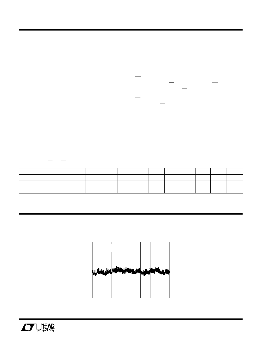
Integral Nonlinearity
CODE
0
INL ERROR (LSBs)
≠1.0
1.0
512
1024
4096
LTC1272 ∑ TPC01
1536
2048
2560
3072
3584
0
V
DD
= 5V
f
CLK
= 4MHz
0
0.5
≠ 0.5