 | –≠–ª–µ–∫—Ç—Ä–æ–Ω–Ω—ã–π –∫–æ–º–ø–æ–Ω–µ–Ω—Ç: LTC1275B | –°–∫–∞—á–∞—Ç—å:  PDF PDF  ZIP ZIP |
1
LTC1273
LTC1275/LTC1276
S
FEATURE
D
U
ESCRIPTIO
s
Single Supply 5V or
±
5V Operation
s
300ksps Sample Rate
s
75mW (Typ) Power Dissipation
s
On-Chip 25ppm/
∞
C Reference
s
Internal Synchronized Clock; No Clock Required
s
High Impedance Analog Input
s
70dB S/(N + D) and 77dB THD at Nyquist
s
±
1/2LSB INL and
±
3/4LSB DNL Max (A Grade)
s
ESD Protected On All Pins
s
24-Pin Narrow DIP and SOL Packages
s
Variety of Input Ranges:
0V to 5V (LTC1273)
±
2.5V (LTC1275)
±
5V (LTC1276)
Effective Bits and Signal to (Noise + Distortion)
vs Input Frequency
LTBiCMOS
TM
is a trademark of Linear Technology Corporation
1
2
3
4
5
6
7
8
9
10
11
12
24
23
22
21
20
19
18
17
16
15
14
13
A
IN
V
REF
AGND
D11
D10
D9
D8
D7
D6
D5
D4
DGND
V
DD
NC
BUSY
CS
RD
HBEN
NC
NC
D0/8
D1/9
D2/10
D3/11
LTC1273
+
0.1
µ
F
10
µ
F
2.42V
V
REF
OUTPUT
ANALOG INPUT
(0V TO 5V)
+
10
µ
F
0.1
µ
F
5V
8- OR 12-BIT
PARALLEL BUS
µ
P CONTROL
LINES
LTC1273/75/76 ∑ TA01
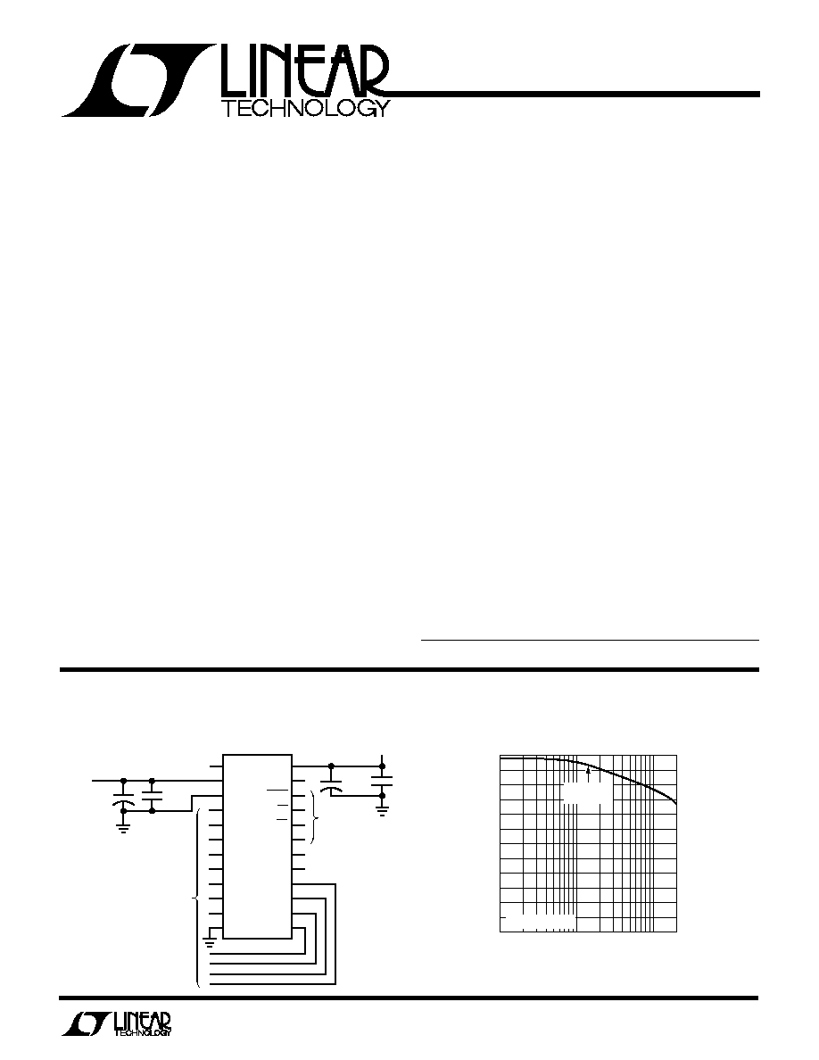
INPUT FREQUENCY (Hz)
10k
0
EFFECTIVE BITS
3
5
7
10
100k
2M
LTC1273/75/76 ∑ TA02
1
4
6
9
12
11
8
2
1M
62
56
74
68
50
S/(N + D) (dB)
f
SAMPLE
= 300kHz
NYQUIST
FREQUENCY
U
S
A
O
PPLICATI
s
High Speed Data Acquisition
s
Digital Signal Processing
s
Multiplexed Data Acquisition Systems
s
Audio and Telecom Processing
s
Spectrum Analysis
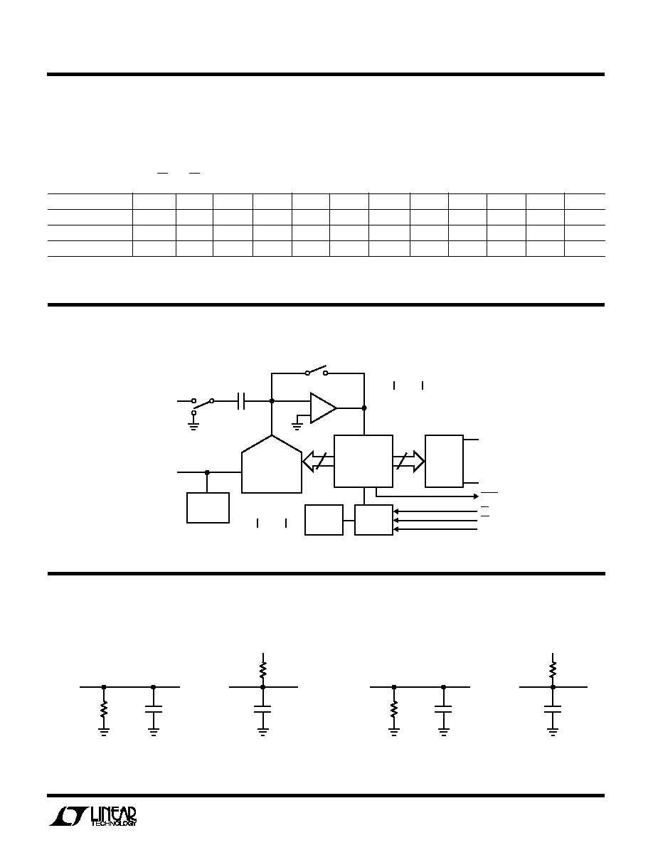
The LTC1273/LTC1275/LTC1276 are 300ksps, sampling
12-bit A/D converters that draw only 75mW from single
5V or
±
5V supplies. These easy-to-use devices come
complete with 600ns sample-and-holds, precision refer-
ences and internally trimmed clocks. Unipolar and bipo-
lar conversion modes provide flexibility for various appli-
cations. They are built with LTBiCMOS
TM
switched ca-
pacitor technology.
These devices have 25ppm/
∞
C (max) internal references.
The LTC1273 converts 0V to 5V unipolar inputs from a
single 5V supply. The LTC1275/LTC1276 convert
±
2.5V
and
±
5V respectively from
±
5V supplies. Maximum DC
specifications include
±
1/2LSB INL,
±
3/4LSB DNL and
25ppm/
∞
C full scale drift over temperature. Outstanding
AC performance includes 70dB S/(N + D) and 77dB THD
at the Nyquist input frequency of 150kHz.
The internal clock is trimmed for 2.7
µ
s maximum conver-
sion time. The clock automatically synchronizes to each
sample command eliminating problems with asynchro-
nous clock noise found in competitive devices. A high
speed parallel interface eases connections to FIFOs, DSPs
and microprocessors.
12-Bit, 300ksps Sampling
A/D Converters with Reference
U
A
O
PPLICATI
TYPICAL
Single 5V Supply, 300ksps, 12-Bit Sampling A/D Converter
2
LTC1273
LTC1275/LTC1276
A
U
G
W
A
W
U
W
A
R
BSOLUTE
XI
TI
S
(Notes 1 and 2)
Supply Voltage (V
DD
) .............................................. 12V
Negative Supply Voltage (V
SS
)
LTC1275/LTC1276.................................. ≠ 6V to GND
Total Supply Voltage (V
DD
to V
SS
)
LTC1275/LTC1276............................................... 12V
Analog Input Voltage (Note 3)
LTC1273 .................................... ≠ 0.3V to V
DD
+ 0.3V
LTC1275/LTC1276.............. V
SS
≠ 0.3V to V
DD
+ 0.3V
Digital Input Voltage (Note 4)
LTC1273 ................................................ ≠ 0.3V to 12V
LTC1275/LTC1276......................... V
SS
≠ 0.3V to 12V
Digital Output Voltage (Note 3)
LTC1273 .................................... ≠ 0.3V to V
DD
+ 0.3V
LTC1275/LTC1276 .............. V
SS
≠ 0.3V to V
DD
+ 0.3V
Power Dissipation ............................................. 500mW
Operating Temperature Range
LTC1273AC, LTC1273BC, LTC1275AC
LTC1275BC, LTC1276AC, LTC1276BC .... 0
∞
C to 70
∞
C
Storage Temperature Range ................ ≠ 65
∞
C to 150
∞
C
Lead Temperature (Soldering, 10 sec) ................. 300
∞
C
W
U
U
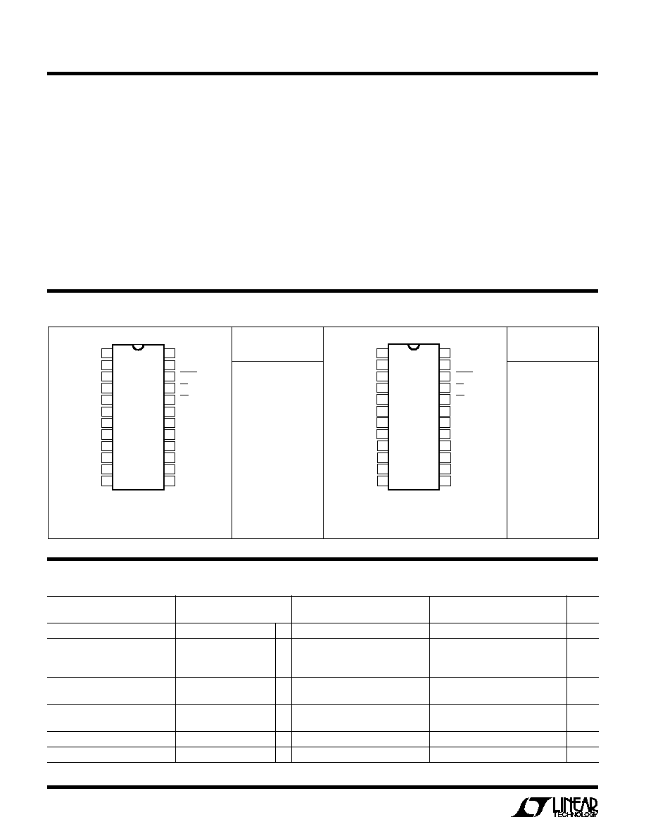
PACKAGE/ORDER I FOR ATIO
ORDER
PART NUMBER
ORDER
PART NUMBER
1
2
3
4
5
6
7
8
9
10
11
12
TOP VIEW
S PACKAGE
24-LEAD PLASTIC SOL
24
23
22
21
20
19
18
17
16
15
14
13
A
IN
V
REF
AGND
D11
D10
D9
D8
D7
D6
D5
D4
DGND
V
DD
NC
BUSY
CS
RD
HBEN
NC
NC
D0/8
D1/9
D2/10
D3/11
N PACKAGE
24-LEAD PLASTIC DIP
1
2
3
4
5
6
7
8
9
10
11
12
TOP VIEW
S PACKAGE
24-LEAD PLASTIC SOL
24
23
22
21
20
19
18
17
16
15
14
13
A
IN
V
REF
AGND
D11
D10
D9
D8
D7
D6
D5
D4
DGND
V
DD
V
SS
BUSY
CS
RD
HBEN
NC
NC
D0/8
D1/9
D2/10
D3/11
N PACKAGE
24-LEAD PLASTIC DIP
T
JMAX
= 110
∞
C,
JA
= 100
∞
C/W (N)
T
JMAX
= 110
∞
C,
JA
= 130
∞
C/W (S)
T
JMAX
= 110
∞
C,
JA
= 100
∞
C/W (N)
T
JMAX
= 110
∞
C,
JA
= 130
∞
C/W (S)
With Internal Reference (Notes 5 and 6)
C
C
HARA TERISTICS
CO
U
VERTER
PARAMETER
CONDITIONS
MIN
TYP
MAX
MIN
TYP
MAX
UNITS
Resolution (No Missing Codes)
q
12
12
Bits
Integral Linearity Error
(Note 7)
±
1/2
±
1
LSB
Commercial
q
±
1/2
±
1
LSB
Military
q
±
3/4
±
1
LSB
Differential Linearity Error
Commercial
q
±
3/4
±
1
LSB
Military
q
±
1
±
1
LSB
Offset Error
(Note 8)
±
3
±
4
LSB
q
±
4
±
6
LSB
Full Scale Error
±
10
±
15
LSB
Full Scale Tempco
I
OUT(REFERENCE)
= 0
q
±
5
±
25
±
10
±
45
ppm/
∞
C
LTC1273A/LTC1275A/LTC1276A
LTC1273B/LTC1275B/LTC1276B
LTC1275ACN
LTC1275BCN
LTC1275ACS
LTC1275BCS
LTC1276ACN
LTC1276BCN
LTC1276ACS
LTC1276BCS
(For MIL Grade:
Contact Factory)
LTC1273ACN
LTC1273BCN
LTC1273ACS
LTC1273BCS
(For MIL Grade:
Contact Factory)
3
LTC1273
LTC1275/LTC1276
SYMBOL
PARAMETER
CONDITIONS
MIN
TYP
MAX
UNITS
S/(N + D) Signal-to-Noise Plus Distortion Ratio
50kHz/150kHz Input Signal
72/70
dB
THD
Total Harmonic Distortion
50kHz/150kHz Input Signal
≠ 83/≠ 74
dB
Up to 5th Harmonic
Peak Harmonic or Spurious Noise
50kHz/150kHz Input Signal
≠ 85/≠ 76
dB
IMD
Intermodulation Distortion
f
IN1
= 29.37kHz, f
IN2
= 32.446kHz
≠ 80
dB
Full Power Bandwidth
4.5
MHz
Full Linear Bandwidth (S/(N + D)
68dB)
200
kHz
SYMBOL
PARAMETER
CONDITIONS
MIN
TYP
MAX
UNITS
V
IN
Analog Input Range (Note 9)
4.95V
V
DD
5.25V (LTC1273)
q
0 to 5
V
4.75V
V
DD
5.25V, ≠ 5.25V
V
SS
≠ 2.45V (LTC1275)
q
±
2.5
V
4.95V
V
DD
5.25V, ≠ 5.25V
V
SS
≠ 4.95V (LTC1276)
q
±
5
V
I
IN
Analog Input Leakage Current
CS = High
q
±
1
µ
A
C
IN
Analog Input Capacitance
Between Conversions (Sample Mode)
50
pF
During Conversions (Hold Mode)
5
pF
t
ACQ
Sample-and-Hold
Commercial
q
600
ns
Acquisition Time
Military
q
1000
ns
(Note 5)
ACCURACY
IC
DY
U
W
A
(Note 5)
LTC1273A/LTC1275A/LTC1276A
LTC1273B/LTC1275B/LTC1276B
PUT
U
I
A
A
U
LOG
LTC1273A/LTC1275A/LTC1276A
LTC1273B/LTC1275B/LTC1276B
PARAMETER
CONDITIONS
MIN
TYP
MAX
MIN
TYP
MAX
UNITS
V
REF
Output Voltage
I
OUT
= 0
2.400
2.420
2.440
2.400
2.420
2.440
V
V
REF
Output Tempco
I
OUT
= 0
q
±
5
±
25
±
10
±
45
ppm/
∞
C
V
REF
Line Regulation
4.95V
V
DD
5.25V
0.01
0.01
LSB/V
≠ 5.25V
V
SS
≠ 4.95V
0.01
0.01
LSB/V
V
REF
Load Regulation
0V
|
I
OUT
|
1mA
2
2
LSB/mA
LTC1273B/LTC1275B/LTC1276B
LTC1273A/LTC1275A/LTC1276A
DIGITAL I PUTS A D DIGITAL OUTPUTS
U
U
LTC1273A/LTC1275A/LTC1276A
LTC1273B/LTC1275B/LTC1276B
SYMBOL
PARAMETER
CONDITIONS
MIN
TYP
MAX
UNITS
V
IH
High Level Input Voltage
V
DD
= 5.25V
q
2.4
V
V
IL
Low Level Input Voltage
V
DD
= 4.95V
q
0.8
V
I
IN
Digital Input Current
V
IN
= 0V to V
DD
q
±
10
µ
A
C
IN
Digital Input Capacitance
5
pF
V
OH
High Level Output Voltage
V
DD
= 4.95V
I
O
= ≠ 10
µ
A
4.7
V
I
O
= ≠ 200
µ
A
q
4.0
V
(Note 5)
I TER AL REFERE CE CHARACTERISTICS
(Note 5)
U
U
U
4
LTC1273
LTC1275/LTC1276
SYMBOL
PARAMETER
CONDITIONS
MIN
TYP
MAX
UNITS
f
SAMPLE(MAX)
Maximum Sampling Frequency
(Note 10)
Commercial
q
300
kHz
Military
q
250
kHz
t
CONV
Conversion Time
Commercial
q
2.7
µ
s
Military
q
3.0
µ
s
t
1
CS to RD Setup Time
q
0
ns
t
2
RD to BUSY Delay
C
L
= 50pF
80
190
ns
Commercial
q
230
ns
Military
q
270
ns
t
3
Data Access Time After RD
C
L
= 20pF
40
90
ns
Commercial
q
110
ns
Military
q
120
ns
C
L
= 100pF
50
125
ns
Commercial
q
150
ns
Military
q
170
ns
t
4
RD Pulse Width
q
t
3
ns
t
5
CS to RD Hold Time
q
0
ns
t
6
Data Setup Time After BUSY
40
70
ns
Commercial
q
90
ns
Military
q
100
ns
DIGITAL I PUTS A D DIGITAL OUTPUTS
U
U
LTC1273A/LTC1275A/LTC1276A
LTC1273B/LTC1275B/LTC1276B
SYMBOL
PARAMETER
CONDITIONS
MIN
TYP
MAX
UNITS
V
OL
Low Level Output Voltage
V
DD
= 4.95V
I
O
= 160
µ
A
0.05
V
I
O
= 1.6mA
q
0.10
0.4
V
I
OZ
High Z Output Leakage D11-D0/8
V
OUT
= 0V to V
DD
, CS High
q
±
10
µ
A
C
OZ
High Z Output Capacitance D11-D0/8
CS High (Note 9 )
q
15
pF
I
SOURCE
Output Source Current
V
OUT
= 0V
≠ 10
mA
I
SINK
Output Sink Current
V
OUT
= V
DD
10
mA
(Note 5)
LTC1273A/LTC1275A/LTC1276A
LTC1273B/LTC1275B/LTC1276B
SYMBOL
PARAMETER
CONDITIONS
MIN
TYP
MAX
UNITS
V
DD
Positive Supply Voltage
LTC1273/LTC1276 (Notes 10, 11)
4.95
5.25
V
LTC1275 (Note 10)
4.75
5.25
V
V
SS
Negative Supply Voltage
LTC1275 (Note 10)
≠ 2.45
≠ 5.25
V
LTC1276 (Notes 10, 11)
≠ 4.95
≠ 5.25
V
I
DD
Positive Supply Current
q
15
25
mA
I
SS
Negative Supply Current
LTC1275/LTC1276
q
0.065
0.200
mA
P
D
Power Dissipation
75
mW
TI I G CHARACTERISTICS
W U
POWER REQUIRE E TS
W U
LTC1273A/LTC1275A/LTC1276A
LTC1273B/LTC1275B/LTC1276B
(Note 5)
See Timing Characteristics Figures (Note 5)
5
LTC1273
LTC1275/LTC1276
SYMBOL
PARAMETER
CONDITIONS
MIN
TYP
MAX
UNITS
t
7
Bus Relinquish Time
20
30
75
ns
Commercial
q
20
85
ns
Military
q
20
90
ns
t
8
HBEN to RD Setup Time
q
0
ns
t
9
HBEN to RD Hold Time
q
0
ns
t
10
Delay Between RD Operations
q
40
ns
t
11
Delay Between Conversions
(Note 10)
500
ns
Commercial
q
600
ns
Military
q
1000
ns
t
12
Aperture Delay of Sample-and-Hold
25
ns
TI I G CHARACTERISTICS
W U
LTC1273A/LTC1275A/LTC1276A
LTC1273B/LTC1275B/LTC1276B
See Timing Characteristics Figures (Note 5)
Note 6: Linearity, offset and full scale specifications apply for unipolar and
bipolar modes.
Note 7: Integral nonlinearity is defined as the deviation of a code from a
straight line passing through the actual endpoints of the transfer curve.
The deviation is measured from the center of the quantization band.
Note 8: Bipolar offset (LTC1275/LTC1276) is the different voltage
measured from ≠ 0.5LSB when the LTC1275/LTC1276 output code flickers
between 0000 0000 0000 and 1111 1111 1111.
Note 9: Guaranteed by design, not subject to test.
Note 10: Recommended operating conditions.
Note11: A
IN
must not exceed V
DD
or fall below V
SS
by more than 50mV for
specified accuracy. Therefore the minimum supply voltage for the
LTC1273 is + 4.95V. The minimum supplies for the LTC1275 are +4.75V
and ≠ 2.45V and the minimum supplies for the LTC1276 are
±
4.95V.
The
q
indicates specifications which apply over the full operating
temperature range; all other limits and typicals T
A
= 25
∞
C.
Note 1: Absolute maximum ratings are those values beyond which the life
of a device may be impaired.
Note 2: All voltage values are with respect to ground with DGND and
AGND wired together (unless otherwise noted).
Note 3: When these pin voltages are taken below V
SS
(ground for
LTC1273) or above V
DD
, they will be clamped by internal diodes. This
product can handle input currents greater than 60mA below V
SS
(ground
for LTC1273) or above V
DD
without latch-up.
Note 4: When these pin voltages are taken below V
SS
(ground for
LTC1273) they will be clamped by internal diodes. This product can handle
input currents greater than 60mA below V
SS
(ground for LTC1273)
without latch-up. These pins are not clamped to V
DD
.
Note 5: V
DD
= 5V (V
SS
= ≠ 5V for LTC1275/LTC1276), 300kHz at 70
∞
C and
250kHz at 125
∞
C, t
r
= t
f
= 5ns unless otherwise specified.
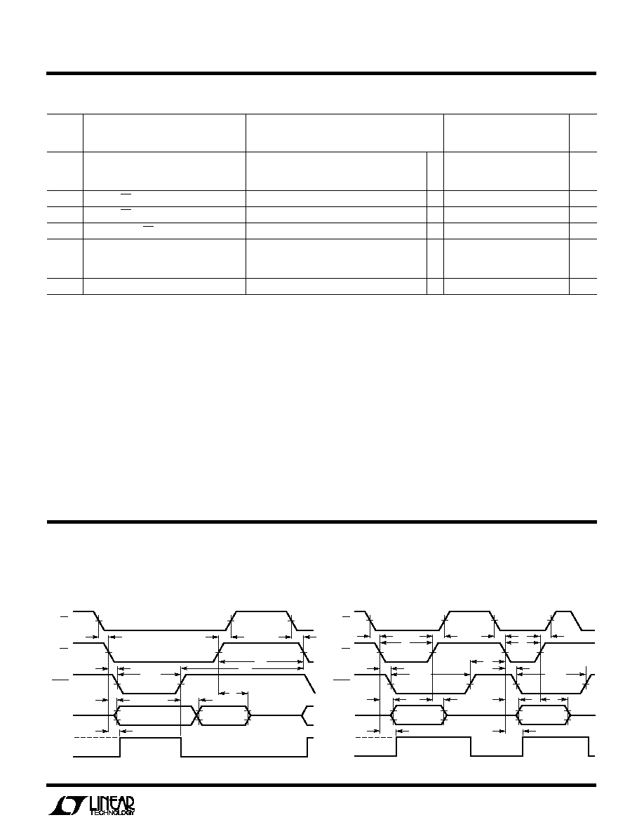
TI I G CHARACTERISTICS
(Note 5)
W U
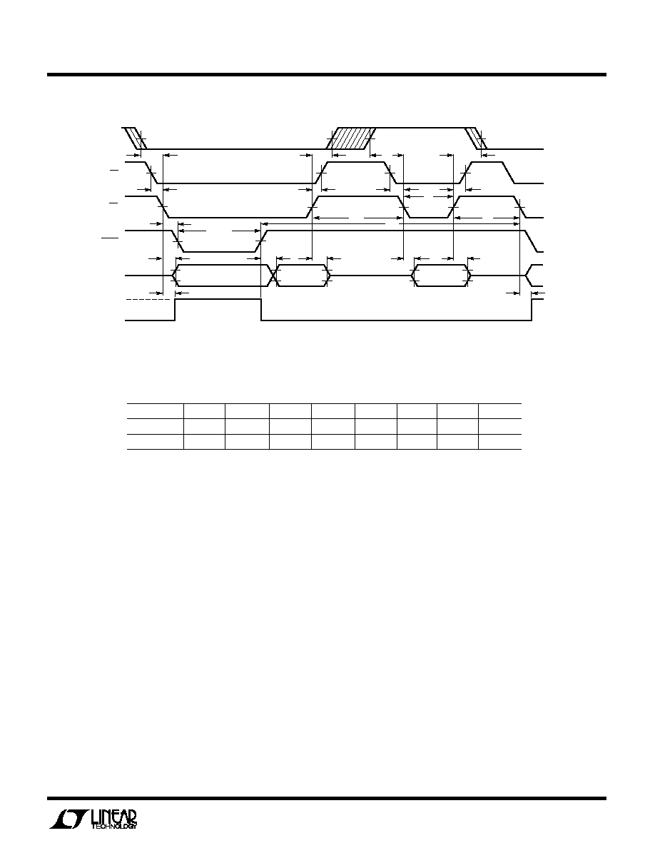
Slow Memory Mode, Parallel Read Timing Diagram
ROM Mode, Parallel Read Timing Diagram
BUSY
DATA
TRACK
OLD DATA
DB11 TO DB0
NEW DATA
DB11 TO DB0
t
1
HOLD
LTC1273/75/76 ∑ TA03
CS
RD
t
5
t
1
t
10
t
11
t
2
t
CONV
t
6
t
3
t
12
t
7
t
1
OLD DATA
DB11 TO DB0
NEW DATA
DB11 TO DB0
DATA
TRACK
HOLD
CS
RD
BUSY
LTC1273/75/76 ∑ TA04
t
5
t
1
t
5
t
4
t
2
t
CONV
t
11
t
2
t
CONV
t
3
t
7
t
3
t
12
t
12
t
4
t
7
6
LTC1273
LTC1275/LTC1276
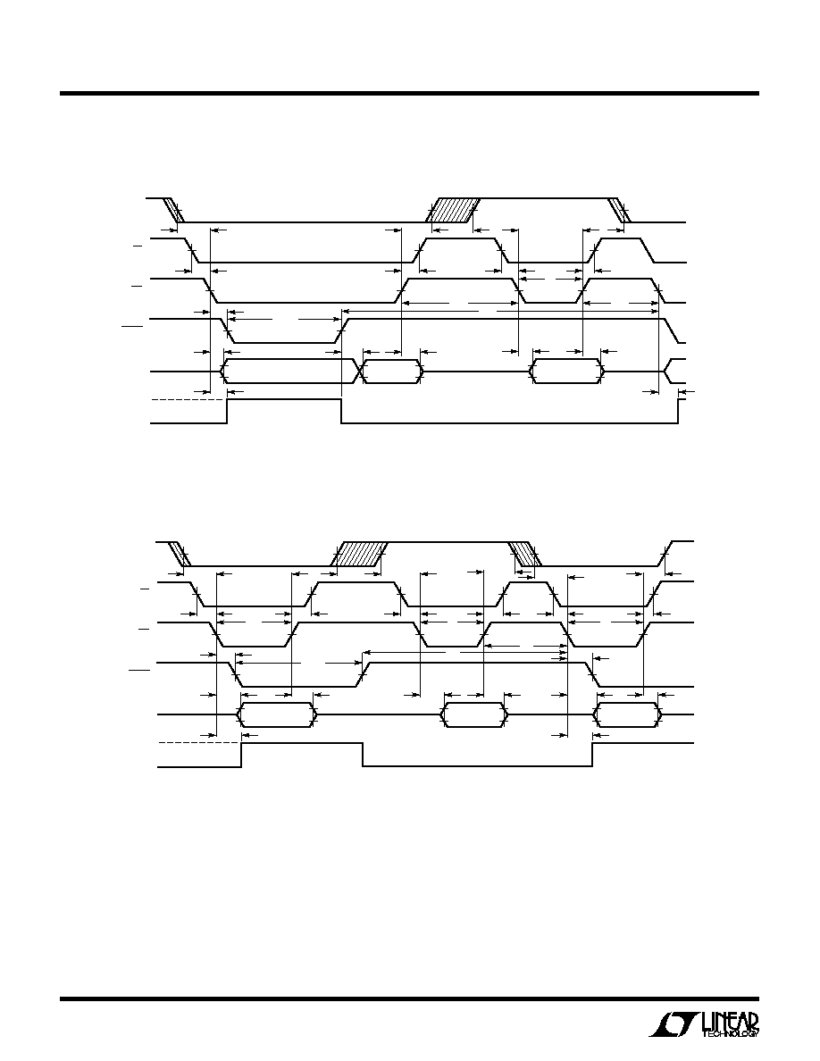
TI I G CHARACTERISTICS
(Note 5)
W U
Slow Memory Mode, Two Byte Read Timing Diagram
CS
RD
BUSY
DATA
TRACK
HOLD
HBEN
OLD DATA
DB7 TO DB0
NEW DATA
DB7 TO DB0
NEW DATA
DB11 TO DB8
LTC1273/75/76 ∑ TA05
t
7
t
8
t
1
t
2
t
3
t
12
t
6
t
7
t
3
t
CONV
t
9
t
8
t
9
t
5
t
4
t
1
t
5
t
10
t
10
t
11
t
12
ROM Mode, Two Byte Read Timing Diagram
CS
RD
BUSY
DATA
TRACK
HOLD
HBEN
OLD DATA
DB7 TO DB0
NEW DATA
DB7 TO DB0
NEW DATA
DB11 TO DB8
LTC1273/75/76 ∑ TA06
t
8
t
9
t
8
t
9
t
8
t
9
t
1
t
4
t
5
t
1
t
4
t
5
t
1
t
5
t
4
t
2
t
CONV
t
11
t
10
t
2
t
7
t
3
t
7
t
3
t
7
t
3
t
12
t
12
7
LTC1273
LTC1275/LTC1276
INPUT FREQUENCY (Hz)
10k
0
EFFECTIVE NUMBER OF BITS
3
5
7
10
100k
2M
LTC1273/75/76 ∑ TPC04
1
4
6
9
12
11
8
2
1M
62
56
74
68
50
S/(N + D) (dB)
f
SAMPLE
= 300kHz
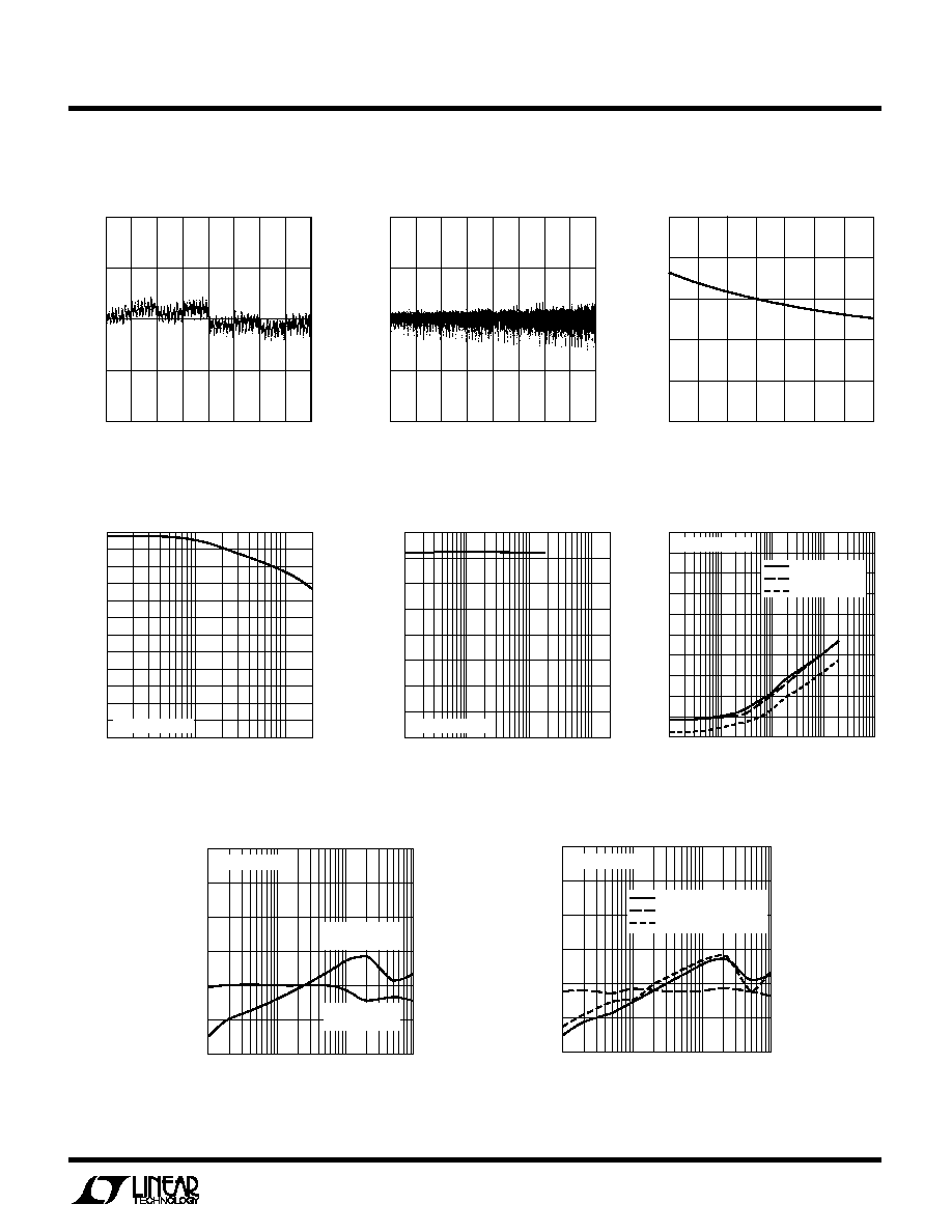
ENOBs and S/(N + D)
vs Input Frequency
INPUT FREQUENCY (Hz)
1k
0
SIGNAL-TO-NOISE RATIO (dB)
10k
1M
LTC1273/75/76 ∑ TPC05
80
100k
f
SAMPLE
= 300kHz
70
60
50
40
30
20
10
Signal-to-Noise Ratio (Without
Harmonics) vs Input Frequency
Distortion vs Input Frequency
C
C
HARA TERISTICS
U
W
A
TYPICAL PERFOR
CE
CODE
0
≠1.0
INL ERROR (LSB)
≠0.5
0
0.5
1.0
512 1024 1536 2048
LTC1273/75/76 ∑ TPC01
2560 3072 3584 4096
Integral Nonlinearity
TEMPERATURE (∞C)
≠50
0
SUPPLY CURRENT (mA)
10
25
0
50
75
LTC1273/75/76 ∑ TPC03
5
20
15
≠25
25
100
125
CODE
0
≠1.0
DNL ERROR (LSB)
≠0.5
0
0.5
1.0
512 1024 1536 2048
LTC1273/75/76 ∑ TPC02
2560 3072 3584 4096
Differential Nonlinearity
Supply Current vs Temperature
Power Supply Feedthrough
vs Ripple Frequency (LTC1273)
RIPPLE FREQUENCY (Hz)
1k
≠120
AMPLITUDE OF POWER SUPPLY FEEDTHROUGH (dB)
≠40
≠20
0
10k
100k
1M
LTC1273/75/76 ∑ TPC07
≠60
≠80
≠100
V
DD
(V
RIPPLE
= 1mV)
DGND
(V
RIPPLE
= 0.1V)
f
SAMPLE
= 300kHz
Power Supply Feedthrough
vs Ripple Frequency (LTC1275/76)
RIPPLE FREQUENCY (Hz)
1k
≠120
AMPLITUDE OF POWER SUPPLY FEEDTHROUGH (dB)
≠40
≠20
0
10k
100k
1M
LTC1273/75/76 ∑ TPC08
≠60
≠80
≠100
f
SAMPLE
= 300kHz
V
DD
(V
RIPPLE
= 1mV)
DGND
(V
RIPPLE
= 0.1V)
V
SS
(V
RIPPLE
= 10mV)
INPUT FREQUENCY (Hz)
≠80
AMPLITUDE (dB BELOW THE FUNDAMENTAL)
≠60
≠40
≠20
0
1k
100k
1M
10M
LTC1273/75/76 ∑ TPC06
≠100
10k
≠90
≠70
≠50
≠30
≠10
f
SAMPLE
= 300kHz
THD
2nd HARMONIC
3rd HARMONIC
8
LTC1273
LTC1275/LTC1276
C
C
HARA TERISTICS
U
W
A
TYPICAL PERFOR
CE
PI FU CTIO S
U
U
U
A
IN
(Pin 1): Analog Input. 0V to 5V (LTC1273),
±
2.5V
(LTC1275) or
±
5V (LTC1276).
V
REF
(Pin 2): +2.42V Reference Output. Bypass to AGND
(10
µ
F tantalum in parallel with 0.1
µ
F ceramic).
AGND (Pin 3): Analog Ground.
D11-D4 (Pins 4 to 11): Three-State Data Outputs.
DGND (Pin 12): Digital Ground.
D3/11-D0/8 (Pins 13 to 16): Three-State Data Outputs.
NC (Pins 17 and 18): No Connection.
HBEN (Pin 19): High Byte Enable Input. This pin is used to
multiplex the internal 12-bit conversion result into the
lower bit outputs (D7-D0/8). See Table 1. HBEN also
disables conversion start when HIGH.
RD (Pin 20): READ Input. This active low signal starts a
conversion when CS and HBEN are low. RD also enables
the output drivers when CS is low.
CS (Pin 21): The CHIP SELECT Input must be low for the
ADC to recognize RD and HBEN inputs.
BUSY (Pin 22): The BUSY Output shows the converter
status. It is low when a conversion is in progress.
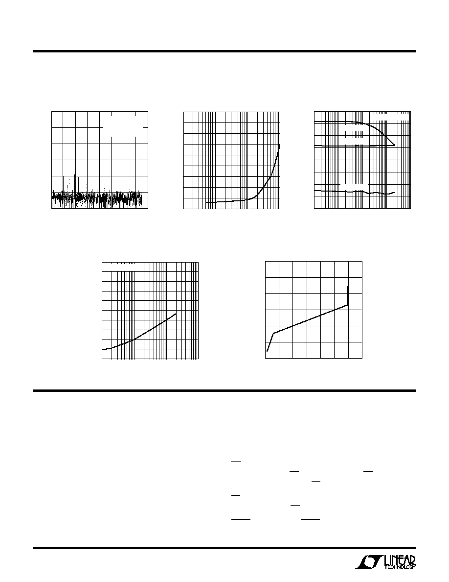
S/(N + D) vs Input Frequency and
Amplitude
Acquisition Time
vs Source Impedance
Intermodulation Distortion Plot
R
SOURCE
(
)
10
2500
ACQUISITION TIME (ns)
3000
3500
4000
4500
100
1k
10k
LTC1273/75/76 ∑ TPC10
2000
1500
500
0
1000
INPUT FREQUENCY (Hz)
20
SIGNAL/(NOISE + DISTORTION) (dB)
40
50
70
80
10k
100k
10M
LTC1273/75/76 ∑ TPC11
0
1k
60
30
10
1M
V
IN
= ≠60dB
V
IN
= ≠20dB
V
IN
= 0dB
f
SAMPLE
= 300kHz
Spurious Free Dynamic Range
vs Input Frequency
Reference Voltage
vs Load Current
LOAD CURRENT (mA)
≠ 5
2.405
REFERENCE VOLTAGE (V)
2.410
2.415
2.420
2.425
2.430
2.435
≠ 4
≠2
≠1
2
LTC1273/75/76 ∑ TPC13
≠3
0
1
INPUT FREQUENCY (Hz)
10k
≠60
SPURIOUS FREE DYNAMIC RANGE (dB)
≠50
≠40
≠30
≠20
100k
1M
10M
LTC1273/75/76 ∑ TPC12
≠70
≠80
≠90
≠100
≠10
0
f
SAMPLE
= 300kHz
FREQUENCY (kHz)
0
≠120
AMPLITUDE (dB)
≠100
≠80
≠60
≠40
40
80
120
160
LTC1273/75/76 ∑ F05
≠20
0
20
60
100
140
f
SAMPLE
= 300kHz
f
IN1
= 29.37kHz
f
IN2
= 32.446kHz
9
LTC1273
LTC1275/LTC1276
PI
U
FU
U
C
U
S
O
TI
V
SS
(Pin 23): Negative Supply. ≠ 5V for LTC1275/LTC1276.
Bypass to AGND with 0.1
µ
F ceramic.
NC (Pin 23): No Connection for LTC1273.
V
DD
(Pin 24): Positive Supply, 5V. Bypass to AGND (10
µ
F
tantalum in parallel with 0.1
µ
F ceramic).
Table 1. Data Bus Output, CS and RD = LOW
Pin 4
Pin 5
Pin 6
Pin 7
Pin 8
Pin 9
Pin 10
Pin 11
Pin 13
Pin 14
Pin 15
Pin 16
MNEMONIC*
D11
D10
D9
D8
D7
D6
D5
D4
D3/11
D2/10
D1/9
D0/8
HBEN = LOW
DB11
DB10
DB9
DB8
DB7
DB6
DB5
DB4
DB3
DB2
DB1
DB0
HBEN = HIGH
DB11
DB10
DB9
DB8
LOW
LOW
LOW
LOW
DB11
DB10
DB9
DB8
*D11...D0/8 are the ADC data output pins.
DB11...DB0 are the 12-bit conversion results, DB11 is the MSB.
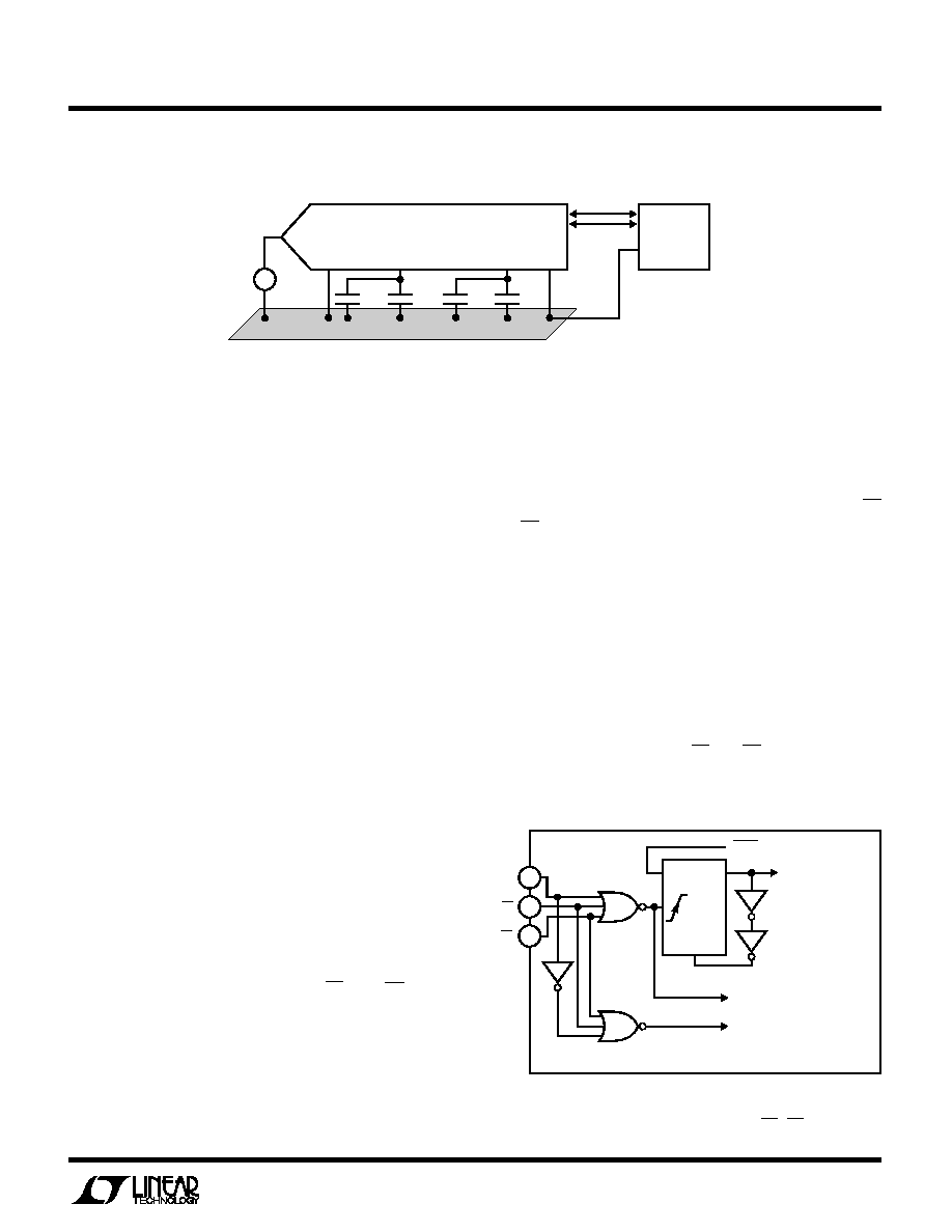
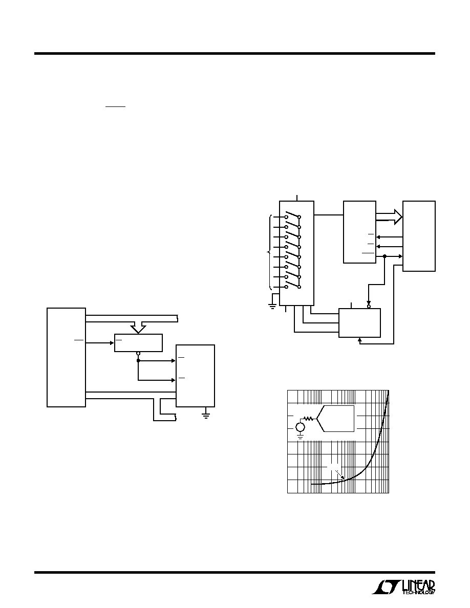
FU TIO AL BLOCK DIAGRA
U
U
W
C
SAMPLE
CONTROL
LOGIC
INTERNAL
CLOCK
SUCCESSIVE
APPROXIMATION
REGISTER
12
12
OUTPUT
LATCHES
∑
∑
∑
D11
D0/8
BUSY
2.42V
REFERENCE
V
REF(OUT)
DGND
AGND
A
IN
SAMPLE
HOLD
SAMPLE
V
SS
(NC ON LTC1273)
V
DD
HBEN
CS
RD
LTC1273/75/76 ∑ FBD
12-BIT
CAPACITIVE
DAC
COMPARATOR
≠
+
TEST CIRCUITS
Load Circuits for Access Time
Load Circuits for Output Float Delay
3k
C
L
DBN
DGND
A) HIGH-Z TO V
OH
(t
3
)
AND V
OL
TO V
OH
(t
6
)
C
L
DBN
3k
5V
B) HIGH-Z TO V
OL
(t
3
)
AND V
OH
TO V
OL
(t
6
)
DGND
1273/75/76 ∑ TA07
3k
10pF
DBN
DGND
A) V
OH
TO HIGH-Z
10pF
DBN
3k
5V
B) V
OL
TO HIGH-Z
DGND
1273/75/76 ∑ TA08
10
LTC1273
LTC1275/LTC1276
U
S
A
O
PPLICATI
W
U
U
I FOR ATIO
CONVERSION DETAILS
The LTC1273/LTC1275/LTC1276 use a successive ap-
proximation algorithm and an internal sample-and-hold
circuit to convert an analog signal to a 12-bit parallel or
2-byte output. The ADCs are complete with a precision
reference and an internal clock. The control logic provides
easy interface to microprocessors and DSPs. (Please refer
to the Digital Interface section for the data format.)
Conversion start is controlled by the CS, RD and HBEN
inputs. At the start of conversion the successive approxi-
mation register (SAR) is reset and the three-state data
outputs are enabled. Once a conversion cycle has begun
it cannot be restarted.
During conversion, the internal 12-bit capacitive DAC
output is sequenced by the SAR from the most significant
bit (MSB) to the least significant bit (LSB). Referring to
Figure 1, the A
IN
input connects to the sample-and-hold
capacitor during the acquire phase, and the comparator
offset is nulled by the feedback switch. In this acquire
phase, a minimum delay of 600ns will provide enough
time for the sample-and-hold capacitor to acquire the
analog signal. During the convert phase, the comparator
feedback switch opens, putting the comparator into the
compare mode. The input switch switches C
SAMPLE
to
ground, injecting the analog input charge onto the sum-
ming junction. This input charge is successively com-
pared with the binary-weighted charges supplied by the
Figure 2. LTC1275 Nonaveraged, 1024 Point FFT Plot
FREQUENCY (kHz)
0
≠120
AMPLITUDE (dB)
≠100
≠80
≠60
≠40
40
80
120
160
LTC1273/75/76 ∑ F02
≠20
0
20
60
100
140
f
SAMPLE
= 300kHz
f
IN
= 29.37kHz
Figure 1. A
IN
Input
V
DAC
LTC1273/75/76 ∑ F01
+
≠
C
DAC
DAC
SAMPLE
HOLD
C
SAMPLE
S
A
R
12-BIT
LATCH
COMPARATOR
SAMPLE
SI
A
IN
capacitive DAC. Bit decisions are made by the high speed
comparator. At the end of a conversion, the DAC output
balances the A
IN
input charge. The SAR contents (a 12-bit
data word) which represent the A
IN
are loaded into the
12-bit output latches.
DYNAMIC PERFORMANCE
The LTC1273/LTC1275/LTC1276 have an exceptionally
high speed sampling capability. FFT (Fast Fourier Trans-
form) test techniques are used to characterize the ADC's
frequency response, distortion and noise at the rated
throughput. By applying a low distortion sine wave and
analyzing the digital output using an FFT algorithm, the
ADC's spectral content can be examined for frequencies
outside the fundamental. Figure 2 shows a typical LTC1275
FFT plot.
Signal-to-Noise Ratio
The Signal-to-Noise plus Distortion Ratio [S/(N + D)] is the
ratio between the RMS amplitude of the fundamental input
frequency to the RMS amplitude of all other frequency
components at the A/D output. The output is band limited
to frequencies from above DC and below half the sampling
frequency. Figure 2 shows a typical spectral content with
a 300kHz sampling rate and a 29kHz input. The dynamic
performance is excellent for input frequencies up to the
Nyquist limit of 150kHz.
11
LTC1273
LTC1275/LTC1276
U
S
A
O
PPLICATI
W
U
U
I FOR ATIO
Effective Number of Bits
The Effective Number of Bits (ENOBs) is a measurement of
the resolution of an ADC and is directly related to the
S/(N + D) by the equation:
N = [S/(N + D) ≠ 1.76]/6.02
where N is the Effective Number of Bits of resolution and
S/(N + D) is expressed in dB. At the maximum sampling
rate of 300kHz the LTC1273/LTC1275/LTC1276 maintain
very good ENOBs up to the Nyquist input frequency of
150kHz. Refer to Figure 3.
INPUT FREQUENCY (Hz)
10k
0
EFFECTIVE BITS
3
5
7
10
100k
2M
LTC1273/75/76 ∑ F03
1
4
6
9
12
11
8
2
1M
62
56
74
68
50
S/(N + D) (dB)
f
SAMPLE
= 300kHz
Figure 3. Effective Bits and Signal to (Noise + Distortion)
vs Input Frequency
Total Harmonic Distortion
Total Harmonic Distortion (THD) is the ratio of the RMS
sum of all harmonics of the input signal to the fundamental
itself. The out-of-band harmonics alias into the frequency
band between DC and half the sampling frequency. THD is
expressed as:
THD = 20log
V
2
2
+ V
3
2
+ V
4
2
... + V
N
2
V
1
where V
1
is the RMS amplitude of the fundamental fre-
quency and V
2
through V
N
are the amplitudes of the
second through Nth harmonics. THD versus input fre-
quency is shown in Figure 4. The LTC1273/LTC1275/
LTC1276 have good distortion performance up to Nyquist
and beyond.
Figure 4. Distortion vs Input Frequency
INPUT FREQUENCY (Hz)
≠80
AMPLITUDE (dB BELOW THE FUNDAMENTAL)
≠60
≠40
≠20
0
1k
100k
1M
10M
LTC1273/75/76 ∑ F04
≠100
10k
≠90
≠70
≠50
≠30
≠10
f
SAMPLE
= 300kHz
THD
2nd HARMONIC
3rd HARMONIC
Intermodulation Distortion
If the ADC input signal consists of more than one spectral
component, the ADC transfer function nonlinearity can
produce intermodulation distortion (IMD) in addition to
THD. IMD is the change in one sinusoidal input caused by
the presence of another sinusoidal input at a different
frequency.
If two pure sine waves of frequencies fa and fb are applied
to the ADC input, nonlinearities in the ADC transfer func-
tion can create distortion products at sum and difference
frequencies of mfa
±
nfb, where m and n = 0, 1, 2, 3, etc.
For example, the 2nd order IMD terms include (fa + fb) and
(fa ≠ fb) while the 3rd order IMD terms include (2fa + fb),
(2fa ≠ fb), (fa + 2fb), and (fa ≠ 2fb). If the two input sine
waves are equal in magnitude, the value (in decibels) of the
2nd order IMD products can be expressed by the following
formula:
IMD (fa ± fb) = 20log
Amplitude at (fa ± fb)
Amplitude at fa
12
LTC1273
LTC1275/LTC1276
U
S
A
O
PPLICATI
W
U
U
I FOR ATIO
Figure 5 shows the IMD performance at a 30kHz input.
FREQUENCY (kHz)
0
≠120
AMPLITUDE (dB)
≠100
≠80
≠60
≠40
40
80
120
160
LTC1273/75/76 ∑ F05
≠20
0
20
60
100
140
f
SAMPLE
= 300kHz
f
IN1
= 29.37kHz
f
IN2
= 32.446kHz
Figure 5. Intermodulation Distortion Plot
Peak Harmonic or Spurious Noise
The peak harmonic or spurious noise is the largest spec-
tral component excluding the input signal and DC. This
value is expressed in decibels relative to the RMS value of
a full scale input signal.
Full Power and Full Linear Bandwidth
The full power bandwidth is that input frequency at which
the amplitude of the reconstructed fundamental is re-
duced by 3dB for a full scale input signal.
The full linear bandwidth is the input frequency at which
the S/(N + D) has dropped to 68dB (11 effective bits). The
LTC1273/LTC1275/LTC1276 have been designed to opti-
mize input bandwidth, allowing ADCs to undersample
input signals with frequencies above the converters' Nyquist
Frequency. The noise floor stays very low at high frequen-
cies; S/(N + D) becomes dominated by distortion at
frequencies far beyond Nyquist.
Driving the Analog Input
The analog inputs of the LTC1273/LTC1275/LTC1276 are
easy to drive. They draw only one small current spike while
charging the sample-and-hold capacitor at the end of
conversion. During conversion the analog input draws no
current. The only requirement is that the amplifier driving
the analog input must settle after the small current spike
before the next conversion starts. Any op amp that settles
in 600ns to small current transients will allow maximum
speed operation. If slower op amps are used, more settling
time can be provided by increasing the time between
conversions. Suitable devices capable of driving the ADCs'
A
IN
input include the LT1190/LT1191, LT1007, LT1220,
LT1223 and LT1224 op amps.
The analog input tolerates source resistance very well.
Here again, the only requirement is that the analog input
must settle before the next conversion starts. For larger
source resistance, full DC accuracy can be obtained if
more time is allowed between conversions. For more
information, see the Acquisition Time vs Source Resis-
tance curve in the Typical Performance Characteristics
section. For optimum frequency domain performance
[e.g., S/(N + D)], keep the source resistance below 100
.
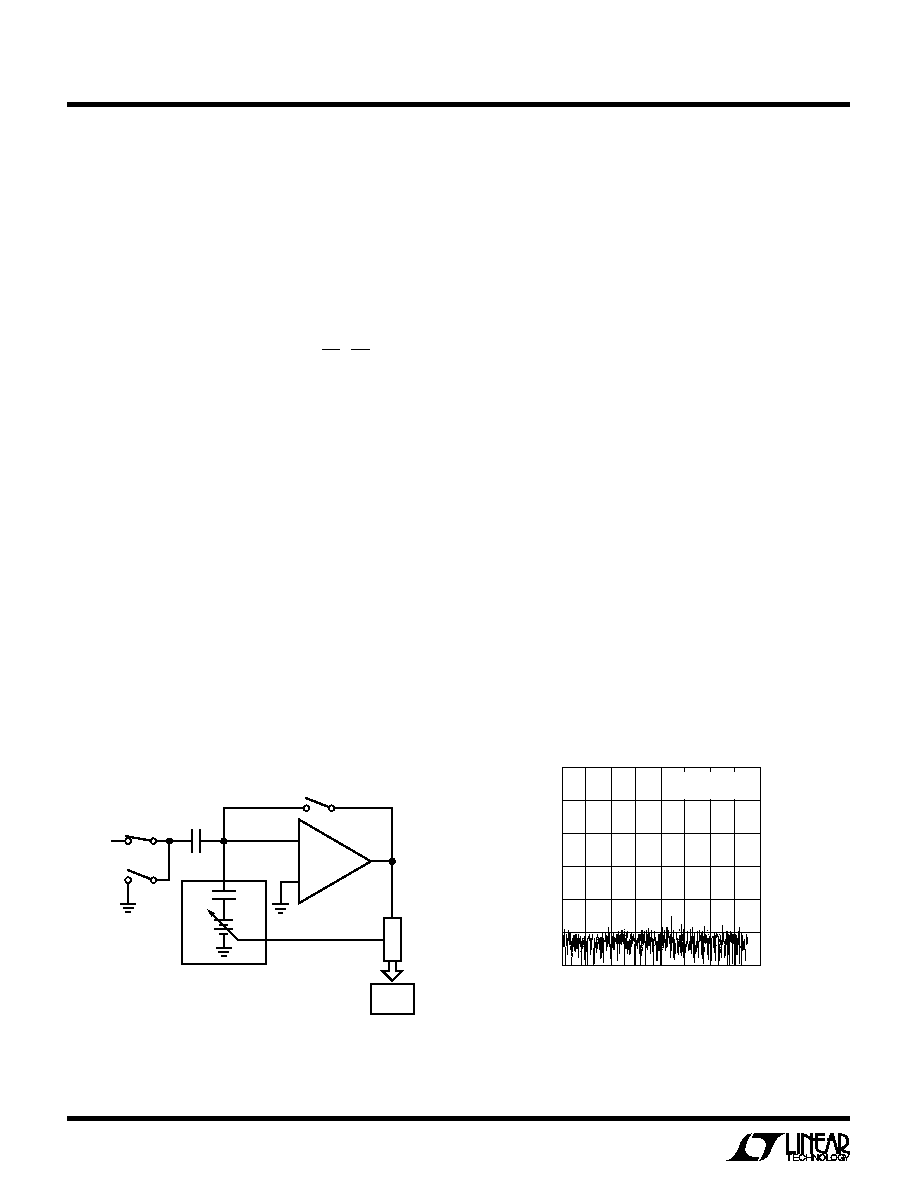
Internal Reference
The LTC1273/LTC1275/LTC1276 have an on-chip, tem-
perature compensated, curvature corrected, bandgap ref-
erence which is factory trimmed to 2.42V. It is internally
connected to the DAC and is available at pin 2 to provide
up to 1mA current to an external load.
For minimum code transition noise the reference output
should be decoupled with a capacitor to filter wideband
noise from the reference (10
µ
F tantalum in parallel with a
0.1
µ
F ceramic).
In the LTC1275, the V
REF
pin can be driven above its
normal value with a DAC or other means to provide input
span adjustment or to improve the reference temperature
drift. Figure 6 shows an LT1006 op amp driving the
V
REF(OUT)
2.45V
3
INPUT RANGE
±1.033V
REF(OUT)
≠
+
LT1006
LTC1275
A
IN
AGND
V
REF
10
µ
F
LTC1273/75/76 ∑ F06
Figure 6. Driving the V
REF
with the LT1006 Op Amp
13
LTC1273
LTC1275/LTC1276
U
S
A
O
PPLICATI
W
U
U
I FOR ATIO
reference pin. The V
REF
pin must be driven to at least
2.45V to prevent conflict with the internal reference. The
reference should be driven to no more than 4.8V to keep
the input span within the
±
5V supplies. In the LTC1273/
LT1276, the input spans are 0V to 5V and
±
5V respec-
tively with the internal reference. Driving the reference is
not recommended on the LTC1273/LTC1276 since the
input spans will exceed the supplies and codes will be lost
at full scale.
Figure 7 shows a typical reference, the LT1019A-2.5
connected to the LTC1275. This will provide an improved
drift (equal to the maximum 5ppm/
∞
C of the LT1019A-2.5)
and a
±
2.582V full scale.
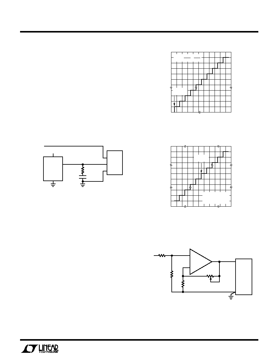
Figure 8. LTC1273 Unipolar Transfer Characteristic
INPUT VOLTAGE (V)
0V
OUTPUT CODE
FS ≠ 1LSB
LTC1273/75/76 ∑ F08
111...111
111...110
111...101
111...100
000...000
000...001
000...010
000...011
1
LSB
1LSB =
FS
4096
=
5V
4096
UNIPOLAR
ZERO
Figure 9. LTC1275/LTC1276 Bipolar Transfer Characteristic
INPUT VOLTAGE (V)
0V
OUTPUT CODE
≠1
LSB
LTC1273/75/76 ∑ F09
011...111
011...110
000...101
000...000
100...000
100...001
111...110
1
LSB
BIPOLAR
ZERO
111...111
FS/2 ≠ 1LSB
≠FS/2
FS = 5V (LTC1275)
FS = 10V (LTC1276)
1LSB = FS/4096
LTC1273
LTC1275
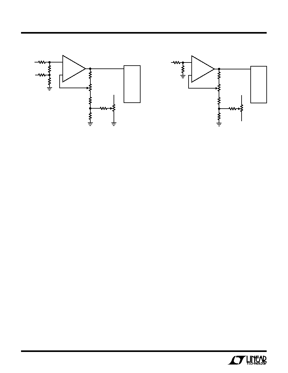
LTC1276
A
IN
AGND
LTC1273/75/76 ∑ F10a
R4
100
FULL SCALE
ADJUST
R3
10k
R2
10k
R1
50
V
1
≠
+
A1
ADDITIONAL PINS OMITTED FOR CLARITY
±20LSB TRIM RANGE
Figure 10a. Full Scale Adjust Circuit
Figure 7. Supplying a 2.5V Reference Voltage
to the LTC1275 with the LT1019A-2.5
3
INPUT RANGE
±2.58V
LTC1275
A
IN
AGND
V
REF
10
µ
F
LTC1273/75/76 ∑ F07
LT1019A-2.5
V
IN
GND
V
OUT
5V
UNIPOLAR/BIPOLAR OPERATION AND ADJUSTMENT
Figure 8 shows the ideal input/output characteristics for
the LTC1273. The code transitions occur midway between
successive integer LSB values (i.e., 1/2LSB, 1 1/2LSBs,
2 1/2LSBs, ... FS ≠ 1 1/2LSBs). The output code is natural
binary with 1LSB = FS/4096 = 5V/4096 = 1.22mV. Figure
9 shows the input/output transfer characteristics for the
LTC1275/LTC1276 in 2's complement format. As stated in
the figure, 1LSB for LTC1275/LTC1276 are 1.22mV and
2.44mV respectively.
Unipolar Offset and Full Scale Adjustment (LTC1273)
In applications where absolute accuracy is important,
offset and full scale errors can be adjusted to zero. Figure
10a shows the extra components required for full scale
error adjustment. If both offset and full scale adjustments
are needed, the circuit in Figure 10b can be used. Offset
14
LTC1273
LTC1275/LTC1276
U
S
A
O
PPLICATI
W
U
U
I FOR ATIO
should be adjusted before full scale. To adjust offset, apply
0.61mV (i.e., 1/2LSB) at the input and adjust the offset trim
until the LTC1273 output code flickers between 0000 0000
0000 and 0000 0000 0001. To adjust full scale, apply an
analog input of 4.99817V (i.e., FS ≠ 1 1/2LSBs or last code
transition) at the input and adjust the full scale trim until
the LTC1273 output code flickers between 1111 1111
1110 and 1111 1111 1111. It should be noted that if
negative ADC offsets need to be adjusted or if an output
swing to ground is required, the op amp in Figure 10b
requires a negative power supply.
Bipolar Offset and Full Scale Adjustment
(LTC1275/LTC1276)
Bipolar offset and full scale errors are adjusted in a similar
fashion to the unipolar case. Figure 10a shows the extra
components required for full scale error adjustment. If both
offset and full scale adjustments are needed, the circuit in
Figure 10c can be used. Again, bipolar offset must be
adjusted before full scale error. Bipolar offset adjustment is
achieved by trimming the offset adjustment of Figure 10c
while the input voltage is 1/2LSB below ground. This is done
by applying an input voltage of ≠ 0.61mV or ≠ 1.22mV
(≠ 0.5LSB for LTC1275 or LTC1276) to the input in Figure
10c and adjusting R8 until the ADC output code flickers
between 0000 0000 0000 and 1111 1111 1111. For full
scale adjustment, an input voltage of 2.49817V or 4.99636V
(FS ≠ 1 1/2LSBs for LTC1275 or LTC1276) is applied to the
Figure 10c. LTC1275/LTC1276 Offset and
Full Scale Adjust Circuit
A
IN
LTC1273/75/76 ∑ F10c
R2
10k
R4
100k
R1
10k
ANALOG
INPUT
±2.5V (LTC1275)
±5V (LTC1276)
R3
100k
5V
R8
20k
OFFSET
ADJUST
R6
200
R5
4.3k
FULL SCALE
ADJUST
R7
100k
≠
+
LTC1275
LTC1276
≠5V
A
IN
LTC1273/75/76 ∑ F10b
R2
10k
R4
100k
R1
10k
10k
5V
R9
20
ANALOG
INPUT
0V TO 5V
R3
100k
5V
R8
10k
OFFSET
ADJUST
R6
400
R5
4.3k
FULL SCALE
ADJUST
R7
100k
≠
+
LTC1273
Figure 10b. LTC1273 Offset and Full Scale Adjust Circuit
input and R5 is adjusted until the output code flickers
between 0111 1111 1110 and 0111 1111 1111.
BOARD LAYOUT AND BYPASSING
The LTC1273/LTC1275/LTC1276 are easy to use. To ob-
tain the best performance from the devices a printed
circuit board is required. Layout for the printed circuit
board should ensure that digital and analog signal lines are
separated as much as possible. In particular, care should
be taken not to run any digital track alongside an analog
signal track. The analog input should be screened by
AGND.
High quality tantalum and ceramic bypass capacitors
should be used at the V
DD
and V
REF
pins as shown in Figure
11. For the LTC1275/LTC1276 a 0.1
µ
F ceramic provides
adequate bypassing for the V
SS
pin. The capacitors must
be located as close to the pins as possible. The traces
connecting the pins and the bypass capacitors must be
kept short and should be made as wide as possible.
Noise: Input signal leads to A
IN
and signal return leads
from AGND (Pin 3) should be kept as short as possible to
minimize input noise coupling. In applications where this
is not possible, a shielded cable between source and ADC
is recommended. Also, since any potential difference in
grounds between the signal source and ADC appears as an
15
LTC1273
LTC1275/LTC1276
U
S
A
O
PPLICATI
W
U
U
I FOR ATIO
Figure 11. Power Supply Grounding Practice
LTC1273/75/76 ∑ F11
A
IN
AGND
V
REF
V
DD
DGND
LTC1273
DIGITAL
SYSTEM
0.1
µ
F
+
≠
ANALOG GROUND PLANE
GROUND CONNECTION
TO DIGITAL CIRCUITRY
ANALOG
INPUT
CIRCUITRY
3
2
24
12
1
0.1
µ
F
10
µ
F
10
µ
F
error voltage in series with the input signal, attention
should be paid to reducing the ground circuit impedances
as much as possible.
A single point analog ground plane separate from the logic
system ground should be established at Pin 3 (AGND) or
as close as possible to the ADC, as shown in Figure 11. Pin
12 (DGND) and all other analog grounds should be con-
nected to this single analog ground point. No other digital
grounds should be connected to this analog ground point.
Low impedance analog and digital power supply common
returns are essential to low noise operation of the ADC and
the width for these traces should be as wide as possible.
In applications where the ADC data outputs and control
signals are connected to a continuously active micropro-
cessor bus, it is possible to get errors in conversion
results. These errors are due to feedthrough from the
microprocessor to the ADC. The problem can be elimi-
nated by forcing the microprocessor into a WAIT state
during conversion or by using three-state buffers to iso-
late the ADC data bus.
DIGITAL INTERFACE
The ADCs are designed to interface with microprocessors
as a memory mapped device. The CS and RD control
inputs are common to all peripheral memory interfacing.
The HBEN input serves as a data byte select for 8-bit
processors and is normally either connected to the micro-
processor address bus or grounded.
Internal Clock
These ADCs have an internal clock that eliminates the need
for synchronization between an external clock and the CS
and RD signals found in other ADCs. The internal clock is
factory trimmed to achieve a typical conversion time of
2.45
µ
s, and a maximum conversion time over the full
operating temperature range of 2.7
µ
s. No external adjust-
ments are required and, with the guaranteed maximum
acquisition time of 600ns, throughput performance of
300ksps is assured.
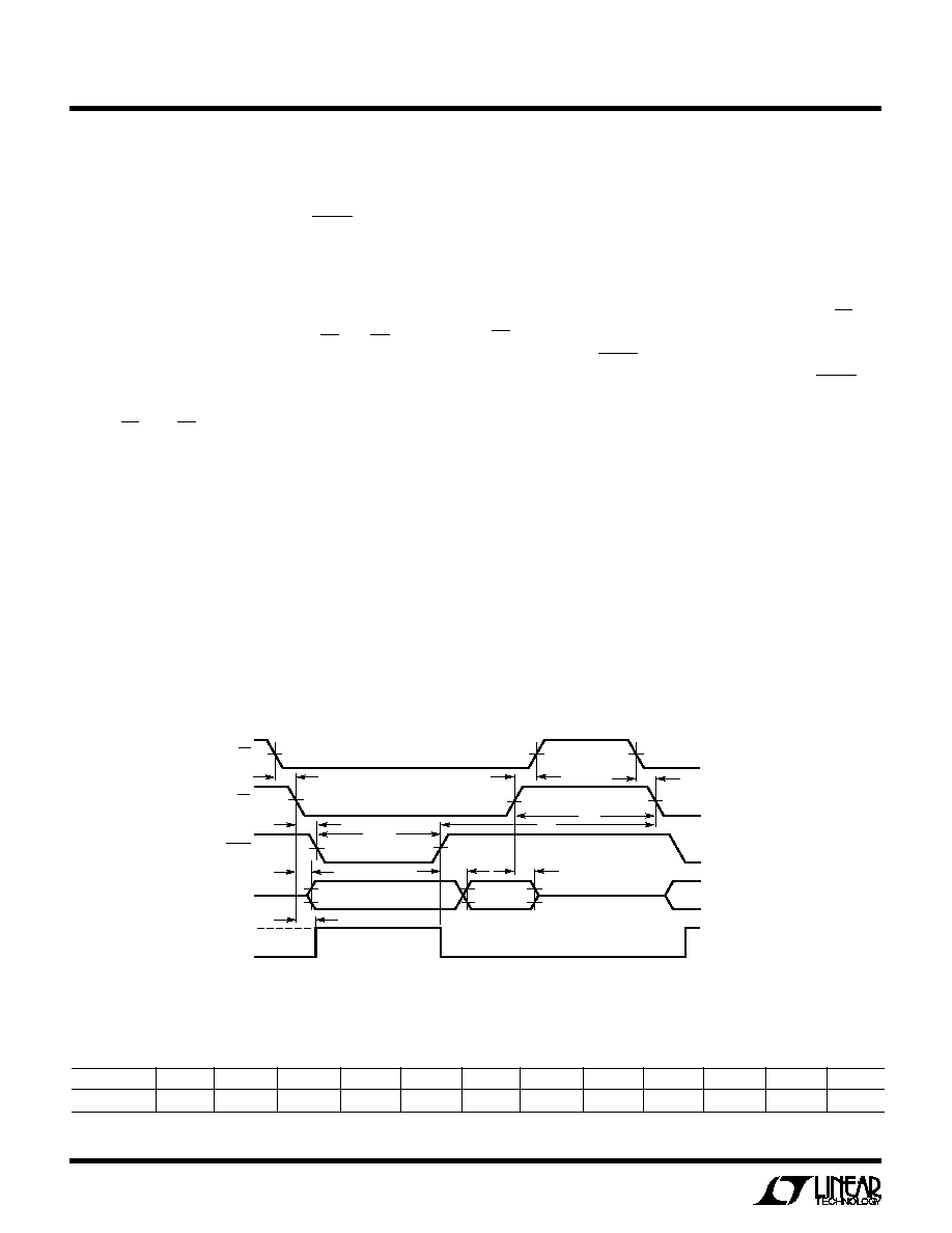
Timing and Control
Conversion start and data read operations are controlled
by three digital inputs: HBEN, CS and RD. Figure 12 shows
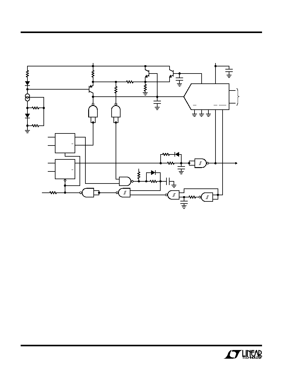
the logic structure associated with these inputs. The three
signals are internally gated so that a logic "0" is required
CONVERSION
START (RISING
EDGE TRIGGER)
LTC1273/75/76 ∑ F12
BUSY
FLIP
FLOP
CLEAR
Q
D
19
21
20
ACTIVE HIGH
ACTIVE HIGH
ENABLE THREE-STATE OUTPUTS
D11....D0/8 = DB11....DB0
ENABLE THREE-STATE OUTPUTS
D11....D8 = DB11....DB8
D7....D4 = LOW
D3/11....D0/8 = DB11....DB8
HBEN
CS
RD
LTC1273/75/76
D11....D0/8 ARE THE ADC DATA OUTPUT PINS
DB11....DB0 ARE THE 12-BIT CONVERSION RESULTS
*
Figure 12. Internal Logic for Control Inputs CS, RD and HBEN
16
LTC1273
LTC1275/LTC1276
U
S
A
O
PPLICATI
W
U
U
I FOR ATIO
t
1
t
2
t
11
t
10
t
6
t
7
t
5
t
1
t
3
t
12
t
CONV
OLD DATA
DB11-DB0
NEW DATA
DB11-DB0
TRACK
HOLD
DATA
BUSY
RD
CS
RD
LTC1273/75/76 ∑ F13
Figure 13. Slow Memory Mode, Parallel Read Timing Diagram
Table 2. Slow Memory Mode, Parallel Read Data Bus Status
Data Outputs
D11
D10
D9
D8
D7
D6
D5
D4
D3/11
D2/10
D1/9
D0/8
Read
DB11
DB10
DB9
DB8
DB7
DB6
DB5
DB4
DB3
DB2
DB1
DB0
8MSBs) where it can be read in two read cycles. The
4MSBs always appear on D11...D8 whenever the three-
state output drivers are turned on.
Slow Memory Mode, Parallel Read (HBEN = LOW)
Figure 13 and Table 2 show the timing diagram and data
bus status for Slow Memory Mode, Parallel Read. CS and
RD going low trigger a conversion and the ADC acknowl-
edges by taking BUSY low. Data from the previous conver-
sion appears on the three-state data outputs. BUSY re-
turns high at the end of conversion when the output
latches have been updated and the conversion result is
placed on data outputs D11...D0/8.
Slow Memory Mode, Two Byte Read
For a two byte read, only 8 data outputs D7...D0/8 are used.
Conversion start procedure and data output status for the
first read operation are identical to Slow Memory Mode,
Parallel Read. See Figure 14 timing diagram and Table 3
data bus status. At the end of the conversion, the low data
byte (D7...D0/8) is read from the ADC. A second READ
operation, with the HBEN high, places the high byte on data
outputs D3/11...D0/8 and disables conversion start. Note
on all three inputs to initiate a conversion. Once initiated it
cannot be restarted until the conversion is complete.
Converter status is indicated by the BUSY output, and this
is low while conversion is in progress.
There are two modes of operation as outlined by the timing
diagrams of Figures 13 to 16. Slow Memory Mode is
designed for microprocessors which can be driven into a
WAIT state. A READ operation brings CS and RD low which
initiates a conversion and data is read when conversion is
complete. The second is the ROM Mode which does not
require microprocessor WAIT states. A READ operation
brings CS and RD low which initiates a conversion and
reads the previous conversion result.
Data Format
The output format can be either a complete parallel load for
16-bit microprocessors or a two byte load for 8-bit micro-
processors. Data is always right justified (i.e., LSB is the
most right-hand bit in a 16-bit word). For a two byte read,
only data outputs D7...D0/8 are used. Byte selection is
governed by the HBEN input which controls an internal
digital multiplexer. This multiplexes the 12-bits of conver-
sion data onto the lower D7...D0/8 outputs (4MSBs or
17
LTC1273
LTC1275/LTC1276
U
S
A
O
PPLICATI
W
U
U
I FOR ATIO
OLD DATA
DB7-DB0
NEW DATA
DB7-DB0
TRACK
HOLD
DATA
BUSY
RD
CS
RD
LTC1273/75/76 ∑ F14
t
8
t
1
t
2
t
3
t
CONV
t
11
t
9
t
8
t
9
t
5
t
1
t
4
t
5
t
10
t
10
t
6
t
7
t
3
t
7
t
12
t
12
HBEN
NEW DATA
DB11-DB8
Figure 14. Slow Memory Mode, Two Byte Read Timing Diagram
Table 3. Slow Memory Mode, Two Byte Read Data Bus Status
Data Outputs
D7
D6
D5
D4
D3/11
D2/10
D1/9
D0/8
First Read
DB7
DB6
DB5
DB4
DB3
DB2
DB1
DB0
Second Read
Low
Low
Low
Low
DB11
DB10
DB9
DB8
that the 4MSBs appear on data output D11...D8 during
both READ operations.
ROM Mode, Parallel Read (HBEN = LOW)
The ROM Mode avoids placing a microprocessor into a
WAIT state. A conversion is started with a READ opera-
tion, and the 12 bits of data from the previous conversion
are available on data outputs D11...D0/8 (see Figure 15
and Table 4). This data may be disregarded if not re-
quired. A second READ operation reads the new data
(DB11...DB0) and starts another conversion. A delay at
least as long as the ADC's conversion time plus the 600ns
minimum delay between conversions must be allowed
between READ operations.
ROM Mode, Two Byte Read
As previously mentioned for a two byte read, only data
outputs D7...D0/8 are used. Conversion is started in the
normal way with a READ operation and the data output
status is the same as the ROM mode, Parallel Read (see
Figure 16 timing diagram and Table 5 data bus status).
Two more READ operations are required to access the new
conversion result. A delay equal at the ADCs' conversion
time must be allowed between conversion start and the
third data READ operation. The second READ operation
with HBEN high disables conversion start and places the
high byte (4MSBs) on data outputs D3/11...D0/8. A third
read operation accesses the low data byte (DB7...DB0)
and starts another conversion. The 4MSBs appear on data
outputs D11...D8 during all three read operations.
MICROPROCESSOR INTERFACING
The LTC1273/LTC1275/LTC1276 allow easy interfac-
ing to digital signal processors as well as modern high
speed, 8-bit or 16-bit microprocessors. Here are sev-
eral examples.
18
LTC1273
LTC1275/LTC1276
U
S
A
O
PPLICATI
W
U
U
I FOR ATIO
OLD DATA
DB7-DB0
NEW DATA
DB11-DB8
TRACK
HOLD
DATA
BUSY
RD
CS
RD
LTC1272 ∑ TA16
t
8
t
1
t
2
t
3
t
CONV
t
11
t
9
t
8
t
9
t
5
t
1
t
4
t
5
t
10
t
3
t
7
t
3
t
7
t
12
t
12
HBEN
t
7
t
4
t
1
t
8
t
9
NEW DATA
DB7-DB0
t
2
t
4
t
5
Figure 16. ROM Mode Two Byte Read Timing Diagram
Table 5. ROM Mode, Two Byte Read Data Bus Status
Data Outputs
D7
D6
D5
D4
D3/11
D2/10
D1/9
D0/8
First Read (Old Data)
DB7
DB6
DB5
DB4
DB3
DB2
DB1
DB0
Second Read (New Data)
Low
Low
Low
Low
DB11
DB10
DB9
DB8
Third Read (New Data)
DB7
DB6
DB5
DB4
DB3
DB2
DB1
DB0
HOLD
t
12
t
7
TRACK
DATA
t
3
t
7
t
3
t
2
t
CONV
t
CONV
t
11
t
1
t
4
t
5
t
4
t
1
t
5
t
2
t
12
OLD DATA
DB11-DB0
NEW DATA
DB11-DB0
BUSY
RD
CS
LTC1273/75/76 ∑ F15
Table 4. ROM Mode, Parallel Read Data Bus Status
Data Outputs
D11
D10
D9
D8
D7
D6
D5
D4
D3/11
D2/10
D1/9
D0/8
First Read (Old Data)
DB11
DB10
DB9
DB8
DB7
DB6
DB5
DB4
DB3
DB2
DB1
DB0
Second Read
DB11
DB10
DB9
DB8
DB7
DB6
DB5
DB4
DB3
DB2
DB1
DB0
Figure 15. ROM Mode, Parallel Read Timing Diagram (HBEN = LOW)

19
LTC1273
LTC1275/LTC1276
U
S
A
O
PPLICATI
W
U
U
I FOR ATIO
TMS320C25
Figure 17 shows an interface between the LTC1273 and
the TMS320C25.
The W/R signal of the DSP initiates a conversion and
conversion results are read from the LTC1273 using the
following instruction:
IN
D, PA
where D is Data Memory Address and PA is the PORT
ADDRESS.
Figure 17. TMS320C25 Interface
DATA BUS
LTC1273/75/76 ∑ F17
ADDRESS BUS
D0
D16
R/W
READY
IS
A1
A16
TMS320C25
ADDRESS
DECODE
EN
D0/8
D11
RD
BUSY
CS
HBEN
LTC1273/75/76
ADDITIONAL PINS OMITTED FOR CLARITY
DATA BUS
LTC1273/75/76 ∑ F18
ADDRESS BUS
D0
D11
R/W
DTACK
AS
A1
A23
MC68000
ADDRESS
DECODE
EN
D0/8
D11
RD
BUSY
CS
HBEN
LTC1273/75/76
ADDITIONAL PINS OMITTED FOR CLARITY
Figure 18. MC68000 Interface
8085A/Z80 Microprocessor
Figure 19 shows an LTC1273 interface for the Z80/8085A.
The LTC1273 is operating in the Slow Memory Mode and
a two byte read is required. Not shown in the figure is the
8-bit latch required to demultiplex the 8085A common
address/data bus. A0 is used to assert HBEN so that an
even address (HBEN = LOW) to the LTC1273 will start a
conversion and read the low data byte. An odd address
(HBEN = HIGH) will read the high data byte. This is
accomplished with the single 16-bit LOAD instruction
below.
For the 8085A
LHLD (B000)
For the Z80
LDHL, (B000)
Figure 19. 8085A and Z80 Interface
DATA BUS
LTC1273/75/76 ∑ F19
ADDRESS BUS
D0
D7
RD
WAIT
MREQ
A0
A15
Z80
8085A
ADDRESS
DECODE
EN
D0/8
D7
RD
BUSY
CS
HBEN
ADDITIONAL PINS OMITTED FOR CLARITY
LTC1273/75/76
A0
MC68000 Microprocessor
Figure 18 shows a typical interface for the MC68000. The
LTC1273 is operating in the Slow Memory Mode. Assum-
ing the LTC1273 is located at address C000, then the
following single 16-bit MOVE instruction both starts a
conversion and reads the conversion result:
Move.W $C000,D0
At the beginning of the instruction cycle when the ADC
address is selected, BUSY and CS assert DTACK so that
the MC68000 is forced into a WAIT state. At the end of
conversion, BUSY returns high and the conversion result
is placed in the D0 register of the microprocessor.
20
LTC1273
LTC1275/LTC1276
U
S
A
O
PPLICATI
W
U
U
I FOR ATIO
This is a two byte read instruction which loads the ADC
data (address B000) into the HL register pair. During the
first read operation, BUSY forces the microprocessor to
WAIT for the LTC1273 conversion. No WAIT states are
inserted during the second read operation when the mi-
croprocessor is reading the high data byte.
TMS32010 Microcomputer
Figure 20 shows an LTC1273/TMS32010 interface. The
LTC1273 is operating in the ROM Mode.
The LTC1273 is mapped at a port address. The following
I/O instruction starts a conversion and reads the previous
conversion result into data memory.
IN A,PA
(PA = PORT ADDRESS)
When conversion is complete, a second I/O instruction
reads the up-to-date data into memory and starts another
conversion. A delay at least as long as the ADC conversion
time must be allowed between I/O instructions.
MUXing with CD4051
The high input impedance of the LTC1273/LTC1275/
LTC1276 provides an easy, cheap, fast, and accurate way
to multiplex many channels of data through one con-
verter. Figure 21 shows a low cost CD4051 connected to
the LTC1275. The LTC1275's input draws no DC input
Figure 20. TMS32010 Interface
DATA BUS
LTC1273/75/76 ∑ F20
PORT ADDRESS BUS
D0
D11
DEN
PA0
PA2
TMS32010
ADDRESS
DECODE
EN
D0/8
D11
RD
CS
HBEN
LTC1273/75/76
LINEAR CIRCUITRY OMITTED FOR CLARITY
current so it can be accurately driven by the unbuffered
MUX. The CD4520 counter increments the MUX channel
after each sample is taken. Figure 22 shows the acquisi-
tion time of LTC1275 vs the source resistance. For a
500
maximum "on" resistance of the CD4051, the
acquisition time of the ADC is not greatly affected. For
larger source resistances, modest increases in acquisi-
tion time must be allowed.
V
DD
5V
V
SS
V
EE
A
B C
≠5V
8 INPUT
CHANNELS
±2.8V
INPUT
VARIES
NO
BUFFER
REQUIRED
D11
D0
∑
∑
∑
CS
RD
BUSY
LTC1275
A
IN
µ
P
OR
DSP
ENABLE
RESET
Q2
Q1
Q0
CD4520
COUNTER
5V
LTC1273/75/76 ∑ F21
CD4051
Figure 21. MUXing the LTC1275 with CD4051
SOURCE RESISTANCE (
)
10
2
ACQUISITION TIME (
µ
s)
3
4
100
1k
10k
LTC1273/75/76 ∑ F22
1
0
LTC1275
A
IN
R
SOURCE
V
IN
500
Figure 22. Acqusition Time of LTC1275 vs Source Resistance
21
LTC1273
LTC1275/LTC1276
U
S
A
O
PPLICATI
W
U
U
I FOR ATIO
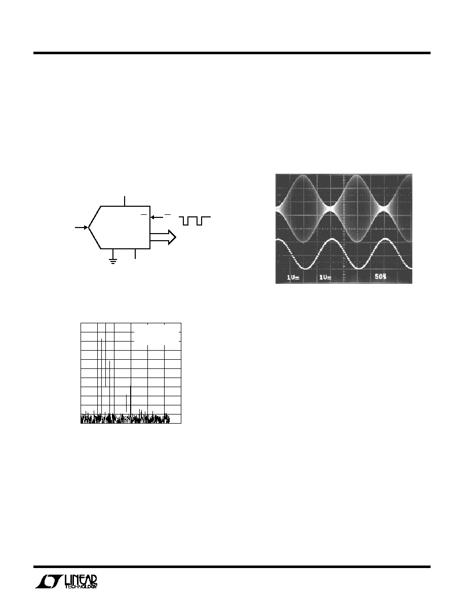
Demodulating a Signal by Undersampling
with LTC1275
Figure 23 shows a 455kHz amplitude modulated input
undersampled by the LTC1275. With a 227.5kHz sample
rate, the converter provides a 100dB noise floor and 68dB
distortion when digitizing the 455kHz AM input.
Figure 24 shows an FFT of the AM signal digitized at
212.5kHz.
A
IN
LTC1275
D11
D0
455kHz
AMPLITUDE
MODULATED
INPUT
RD
RD
≠5V
227.5kHz
SAMPLE RATE
5V
LTC1273/75/76 ∑ F23
DATA OUTPUT
Figure 23. A 455kHz Amplitude Modulated Input
Undersampled by the LTC1275
FREQUENCY (kHz)
0
≠110
AMPLITUDE (dB)
≠90
≠70
≠50
≠30
20
40
60
80
LTC1273/75/76 ∑ F24
100
120
≠10
≠100
≠80
≠60
≠40
≠20
0
f
SAMPLE
= 212.5kHz
f
IN
= 454.8kHz
f
MOD
= 5.03kHz
Figure 24. 455kHz Input Voltage Modulated by a 5kHz Signal
A time domain view of the demodulation is shown in Figure
25. The top trace shows the 455kHz waveform modulated
by a ≠ 6dB, 5kHz signal. The bottom trace shows the
demodulated signal produced by the LTC1275 recon-
structed through a 12-bit DAC. The resultant frequency is
5kHz with a sample rate of 227.5kHz. There are roughly 45
points per cycle.
Figure 25. 455kHz AM Signal Demodulated to 10.5 ENOBs
DEMODULATED
5kHz OUTPUT
455kHz
AM SIGNAL
50
µ
s/DIV
LTC1273/75/76 ∑ F27
1V/DIV
1V/DIV
100ps Resolution
Time Measurement with LTC1273
Figure 26 shows a circuit that precisely measures the
difference in time between two events. It has a 400ns full
scale and 100ps resolution. The start signal releases the
ramp generator made up of the PNP current source and
the 250pF capacitor. The circuit ramps until the stop
signal shuts off the current source. The final value of the
ramp represents the time between the start and stop
events. The LTC1273 digitizes this final value and outputs
the digital data.
22
LTC1273
LTC1275/LTC1276
U
S
A
O
PPLICATI
W
U
U
I FOR ATIO
Figure 26.
Time Measurement with the LTC1273
V
SS
GND
A
IN
REF
OUT
V
DD
LTC1273
CS
RD BUSY
12-BIT
DATA OUTPUT
10
µ
F
2N2369
20k
400k
250pF
POLYSTYRENE
620
2N5771
65
7V
5V
74HC03
65
45.3
45.3
1N457
LM134
D
CLK
Q
Q
CLR
D
CLK
Q
Q
CLR
1k
5V
5V
START
5V
STOP
DATA LATCH
SIGNAL
10
µ
F
1k
5V
100k
1N4148
0.001
µ
F
10k
1N457
74HC74
10pF
1k
1N4148
100pF
10k
LTC1273/75/76 ∑ F26
2N2369
23
LTC1273
LTC1275/LTC1276
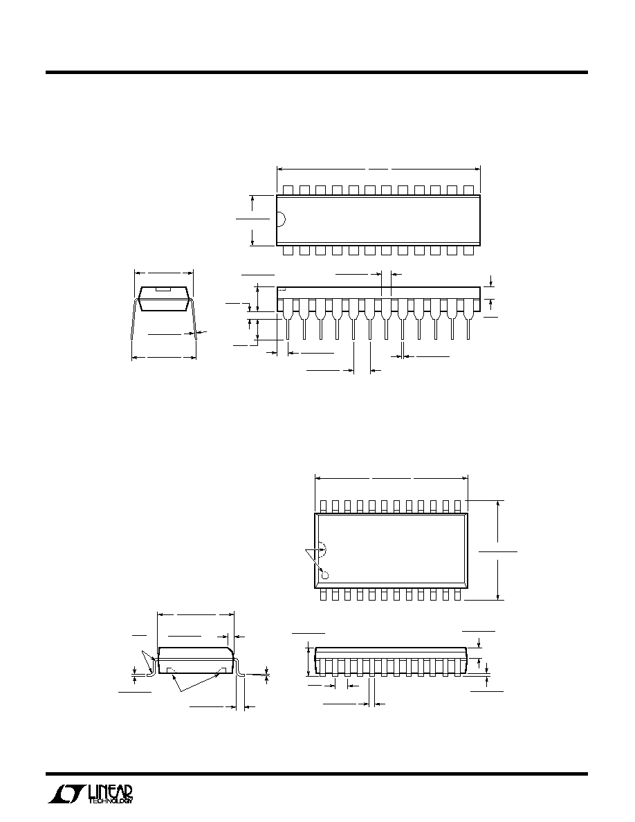
N Package
24-Lead Plastic DIP
U
PACKAGE DESCRIPTIO
Dimensions in inches (millimeters) unless otherwise noted.
NOTE 1
0.598 ≠ 0.614
(15.190 ≠ 15.600)
(NOTE 2)
22
21
20
19
18
17
16
15
1
2
3
4
5
6
7
8
0.394 ≠ 0.419
(10.007 ≠ 10.643)
9
10
13
14
11
12
23
24
0.037 ≠ 0.045
(0.940 ≠ 1.143)
0.004 ≠ 0.012
(0.102 ≠ 0.305)
0.093 ≠ 0.104
(2.362 ≠ 2.642)
0.050
(1.270)
TYP
0.014 ≠ 0.019
(0.356 ≠ 0.482)
0∞ ≠ 8∞ TYP
NOTE 1
0.009 ≠ 0.013
(0.229 ≠ 0.330)
0.016 ≠ 0.050
(0.406 ≠ 1.270)
0.291 ≠ 0.299
(7.391 ≠ 7.595)
(NOTE 2)
◊
45
∞
0.010 ≠ 0.029
(0.254 ≠ 0.737)
0.005
(0.127)
RAD MIN
NOTE:
1. PIN 1 IDENT, NOTCH ON TOP AND CAVITIES ON THE BOTTOM OF PACKAGES ARE THE MANUFACTURING OPTIONS.
THE PART MAY BE SUPPLIED WITH OR WITHOUT ANY OF THE OPTIONS.
2. THESE DIMENSIONS DO NOT INCLUDE MOLD FLASH OR PROTRUSIONS.
MOLD FLASH OR PROTRUSIONS SHALL NOT EXCEED 0.006 INCH (0.15mm).
S Package
24-Lead Plastic SOL
0.260 ± 0.010
(6.604 ± 0.254)
1.265
(32.131)
1
2
3
4
5
6
7
8
9
10
19
11
12
13
14
16
15
17
18
20
21
22
23
24
0.015
(0.381)
MIN
0.125
(3.175)
MIN
0.130 ± 0.005
(3.302 ± 0.127)
0.065
(1.651)
TYP
0.045 ≠ 0.065
(1.143 ≠ 1.651)
0.018 ± 0.003
(0.457 ± 0.076)
0.050 ≠ 0.085
(1.27 ≠ 2.159)
0.100 ± 0.010
(2.540 ± 0.254)
0.009 ≠ 0.015
(0.229 ≠ 0.381)
0.300 ≠ 0.325
(7.620 ≠ 8.255)
0.325
+0.025
≠0.015
+0.635
≠0.381
8.255
(
)
Information furnished by Linear Technology Corporation is believed to be accurate and reliable.
However, no responsibility is assumed for its use. Linear Technology Corporation makes no represen-
tation that the interconnection of its circuits as described herein will not infringe on existing patent rights.

24
LTC1273
LTC1275/LTC1276
Linear Technology Corporation
1630 McCarthy Blvd., Milpitas, CA 95035-7487
(408) 432-1900
q
FAX
: (408) 434-0507
q
TELEX
: 499-3977
©
LINEAR TECHNOLOGY CORPORATION 1993
LT/GP 0893 10K REV 0
World Headquarters
Linear Technology Corporation
1630 McCarthy Blvd.
Milpitas, CA 95035-7487
Phone: (408) 432-1900
FAX: (408) 434-0507
U.S. Area Sales Offices
NORTHEAST REGION
Linear Technology Corporation
One Oxford Valley
2300 E. Lincoln Hwy.,Suite 306
Langhorne, PA 19047
Phone: (215) 757-8578
FAX: (215) 757-5631
Linear Technology Corporation
266 Lowell St., Suite B-8
Wilmington, MA 01887
Phone: (508) 658-3881
FAX: (508) 658-2701
SOUTHWEST REGION
Linear Technology Corporation
22141 Ventura Blvd.
Suite 206
Woodland Hills, CA 91364
Phone: (818) 703-0835
FAX: (818) 703-0517
NORTHWEST REGION
Linear Technology Corporation
782 Sycamore Dr.
Milpitas, CA 95035
Phone: (408) 428-2050
FAX: (408) 432-6331
SOUTHEAST REGION
Linear Technology Corporation
17060 Dallas Parkway
Suite 208
Dallas, TX 75248
Phone: (214) 733-3071
FAX: (214) 380-5138
CENTRAL REGION
Linear Technology Corporation
Chesapeake Square
229 Mitchell Court, Suite A-25
Addison, IL 60101
Phone: (708) 620-6910
FAX: (708) 620-6977
International Sales Offices
FRANCE
Linear Technology S.A.R.L.
Immeuble "Le Quartz"
58 Chemin de la Justice
92290 Chatenay Malabry
France
Phone: 33-1-41079555
FAX: 33-1-46314613
GERMANY
Linear Techonolgy GMBH
Untere Hauptstr. 9
D-85386 Eching
Germany
Phone: 49-89-3197410
FAX: 49-89-3194821
JAPAN
Linear Technology KK
5F YZ Bldg.
Iidabashi, Chiyoda-Ku
Tokyo, 102 Japan
Phone: 81-3-3237-7891
FAX: 81-3-3237-8010
KOREA
Linear Technology Korea Branch
Namsong Building, #505
Itaewon-Dong 260-199
Yongsan-Ku, Seoul
Korea
Phone: 82-2-792-1617
FAX: 82-2-792-1619
SINGAPORE
Linear Technology Pte. Ltd.
101 Boon Keng Road
#02-15 Kallang Ind. Estates
Singapore 1233
Phone: 65-293-5322
FAX: 65-292-0398
TAIWAN
Linear Technology Corporation
Rm. 801, No. 46, Sec. 2
Chung Shan N. Rd.
Taipei, Taiwan, R.O.C.
Phone: 886-2-521-7575
FAX: 886-2-562-2285
UNITED KINGDOM
Linear Technology (UK) Ltd.
The Coliseum, Riverside Way
Camberley, Surrey GU15 3YL
United Kingdom
Phone: 44-276-677676
FAX: 44-276-64851
06/24/93