 | ÐлекÑÑоннÑй компоненÑ: LTC1282B | СкаÑаÑÑ:  PDF PDF  ZIP ZIP |
/home/web/doc/html/liner/177715
1
LTC1282
S
FEATURE
D
U
ESCRIPTIO
The LTC
®
1282 is a 6
µ
s, 140ksps, sampling 12-bit A/D
converter that draws only 12mW from a single 3V or dual
±
3V supply. This easy-to-use device comes complete with
1.14
µ
s sample-and-hold, precision reference and inter-
nally trimmed clock. Unipolar and bipolar conversion
modes provide flexibility for various applications. They are
built with LTBiCMOS
TM
switched capacitor technology.
The LTC1282 has a 25ppm/
°
C (max) internal reference
and converts 0V to 2.5V unipolar inputs from a single 3V
supply. With
±
3V supplies its input range is
±
1.25V with
two's complement output format. Maximum DC specifica-
tions include
±
0.5LSB INL,
±
0.75LSB DNL and 25ppm/
°
C
full-scale drift over temperature. Outstanding AC perfor-
mance includes 69dB S/(N + D) and 77dB THD at the
Nyquist input frequency of 70kHz.
The internal clock is trimmed for 6
µ
s maximum conver-
sion time. The clock automatically synchronizes to each
sample command eliminating problems with asynchro-
nous clock noise found in competitive devices. A high
speed parallel interface eases connections to FIFOs, DSPs
and microprocessors.
3V 140ksps 12-Bit
Sampling A/D Converter
with Reference
s
Single Supply 3V or
±
3V Operation
s
140ksps Throughput Rate
s
12mW (Typ) Power Dissipation
s
On-Chip 25ppm/
°
C Reference
s
Internal Synchronized Clock; No Clock Required
s
High Impedance Analog Input
s
69dB S/(N + D) and 77dB THD at Nyquist
s
±
0.5LSB INL and
±
0.75LSB DNL Max (A Grade)
s
2.7V Guaranteed Minimum Supply Voltage
s
ESD Protected On All Pins
s
24-Pin Narrow PDIP and SW Packages
s
0V to 2.5V or
±
1.25V Input Ranges
U
S
A
O
PPLICATI
s
3V Powered Systems
s
High Speed Data Acquisition
s
Digital Signal Processing
s
Multiplexed Data Acquisition Systems
s
Audio and Telecom Processing
s
Spectrum Analysis
INPUT FREQUENCY (Hz)
1k
0
ENOBs (EFFECTIVE NUMBER OF BITS)
3
5
7
10
10k
LTC1282 · TA02
1
4
6
9
12
11
8
2
100k
62
56
74
68
50
S/(N + D) (dB)
f
SAMPLE
= 140kHz
NYQUIST
FREQUENCY
Effective Bits and Signal-to-(Noise + Distortion)
vs Input Frequency
, LTC and LT are registered trademarks of Linear Technology Corporation.
LTBiCMOS is a trademark of Linear Technology Corporation
1
2
3
4
5
6
7
8
9
10
11
12
24
23
22
21
20
19
18
17
16
15
14
13
A
IN
V
REF
AGND
D11(MSB)
D10
D9
D8
D7
D6
D5
D4
DGND
V
DD
V
SS
BUSY
CS
RD
HBEN
NC
NC
D0/8
D1/9
D2/10
D3/11
LTC1282
+
0.1
µ
F
10
µ
F
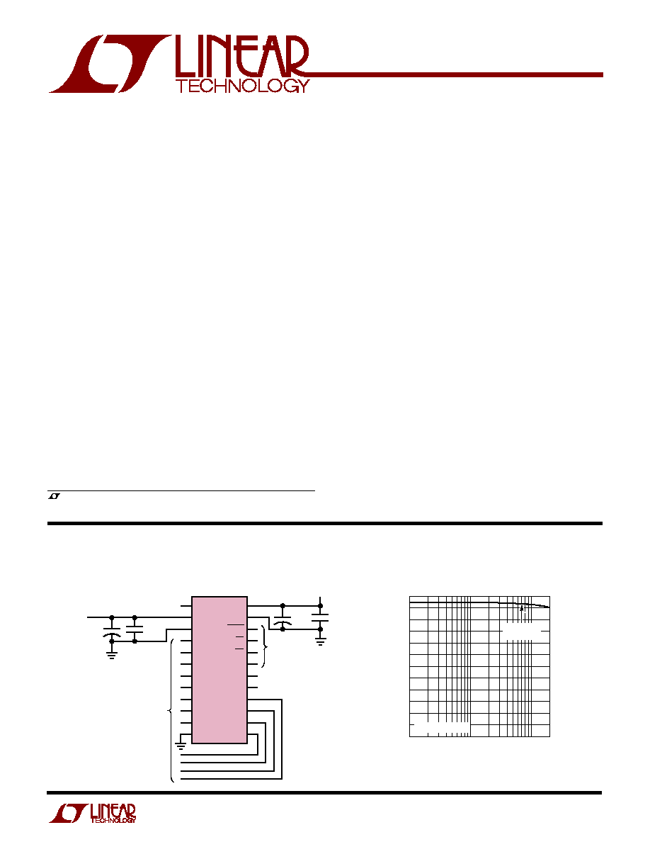
1.20V
V
REF
OUTPUT
ANALOG INPUT
(0V TO 2.5V)
+
10
µ
F
0.1
µ
F
3V
8- OR 12-BIT
PARALLEL BUS
µ
P CONTROL
LINES
1282 TA01
Single 3V Supply, 140ksps, 12-Bit Sampling A/D Converter
U
A
O
PPLICATI
TYPICAL
2
LTC1282
A
U
G
W
A
W
U
W
A
R
BSOLUTE
XI
TI
S
(Notes 1 and 2)
Supply Voltage (V
DD
) .............................................. 12V
Negative Supply Voltage (V
SS
)................... 6V to GND
Total Supply Voltage (V
DD
to V
SS
) .......................... 12V
Analog Input Voltage
(Note 3) .............................. V
SS
0.3V to V
DD
+ 0.3V
Digital Input Voltage (Note 4) ........... V
SS
0.3V to 12V
Digital Output Voltage
(Note 3) .............................. V
SS
0.3V to V
DD
+ 0.3V
Power Dissipation ............................................. 500mW
Specified Temperature Range (Note 14) ..... 0
°
C to 70
°
C
Operating Temperature Range
LTC1282AC, LTC1282BC ......................... 0
°
C to 70
°
C
Storage Temperature Range ................ 65
°
C to 150
°
C
Lead Temperature (Soldering, 10 sec)................. 300
°
C
W
U
U
PACKAGE/ORDER I FOR ATIO
T
JMAX
= 110
°
C,
JA
= 100
°
C/W (N)
T
JMAX
= 110
°
C,
JA
= 130
°
C/W (SW)
ORDER
PART NUMBER
LTC1282ACN
LTC1282BCN
LTC1282ACSW
LTC1282BCSW
Consult factory for Industrial and Military grade parts. (Note 14)
SYMBOL
PARAMETER
CONDITIONS
MIN
TYP
MAX
UNITS
S/(N + D)
Signal-to-Noise Plus Distortion Ratio
10kHz/70kHz Input Signal
71/69
dB
THD
Total Harmonic Distortion
10kHz/70kHz Input Signal, Up to 5th Harmonic
82/ 77
dB
Peak Harmonic or Spurious Noise
10kHz/70kHz Input Signal
82/ 77
dB
IMD
Intermodulation Distortion
f
IN1
= 19.0kHz, f
IN2
= 20.6kHz
78
dB
Full Power Bandwidth
4
MHz
Full Linear Bandwidth (S/(N + D)
68dB)
200
kHz
With Internal Reference (Notes 5 and 6)
C
C
HARA TERISTICS
CO
U
VERTER
PARAMETER
CONDITIONS
MIN
TYP
MAX
MIN
TYP
MAX
UNITS
Resolution (No Missing Codes)
q
12
12
Bits
Integral Linearity Error
(Note 7)
±
1/2
±
1
LSB
Commercial
q
±
1/2
±
1
LSB
Military
q
±
3/4
±
1
LSB
Differential Linearity Error
Commercial
q
±
3/4
±
1
LSB
Military
q
±
1
±
1
LSB
Offset Error
(Note 8)
±
3
±
4
LSB
q
±
4
±
6
LSB
Gain Error
±
10
±
15
LSB
Gain Error Tempco
I
OUT(REF)
= 0
q
±
5
±
25
±
10
±
45
ppm/
°
C
Power Supply Rejection
(Note 9) V
DD
±
10%
±
0.3
±
0.3
LSB
(Note 10) V
SS
±
10%
±
0.1
±
0.1
LSB
LTC1282A
LTC1282B
ACCURACY
IC
DY
U
W
A
LTC1282A/LTC1282B
(Note 5)
1
2
3
4
5
6
7
8
9
10
11
12
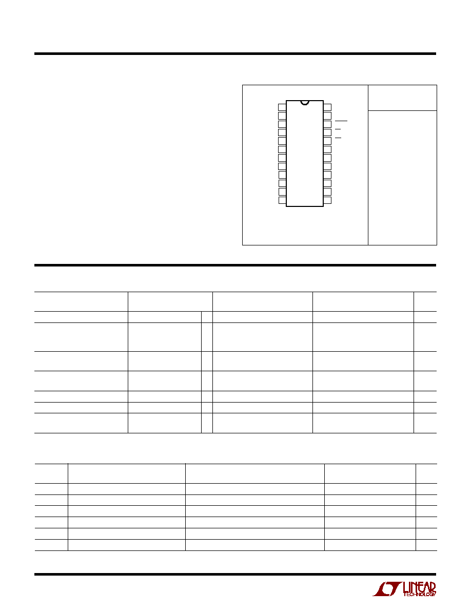
TOP VIEW
SW PACKAGE
24-LEAD PLASTIC SO WIDE
24
23
22
21
20
19
18
17
16
15
14
13
A
IN
V
REF
AGND
D11 (MSB)
D10
D9
D8
D7
D6
D5
D4
DGND
V
DD
V
SS
BUSY
CS
RD
HBEN
NC
NC
D0/8
D1/9
D2/10
D3/11
N PACKAGE
24-LEAD PDIP
3
LTC1282
SYMBOL
PARAMETER
CONDITIONS
MIN
TYP
MAX
UNITS
V
IN
Analog Input Range (Note 11)
2.7V
V
DD
3.6V (Unipolar Mode)
0 to 2.5
V
3V
V
DD
3.6V, 3.3V
V
SS
2.5V (Bipolar Mode)
±
1.25
V
I
IN
Analog Input Leakage Current
CS = High
q
±
1
µ
A
C
IN
Analog Input Capacitance
Between Conversions (Sample Mode)
63
pF
During Conversions (Hold Mode)
5
pF
t
ACQ
Sample-and-Hold
Commercial
q
0.45
1.14
µ
s
Acquisition Time
Military
q
1.5
µ
s
(Note 5)
PUT
U
I
A
A
U
LOG
LTC1282A/LTC1282B
PARAMETER
CONDITIONS
MIN
TYP
MAX
MIN
TYP
MAX
UNITS
V
REF
Output Voltage
I
OUT
= 0
1.1900
1.200
1.210
1.190
1.200
1.210
V
V
REF
Output Tempco
I
OUT
= 0
q
±
5
±
25
±
10
±
45
ppm/
°
C
V
REF
Line Regulation
2.7V
V
DD
3.6V
0.55
0.55
LSB/V
3.6V
V
SS
2.7V
0.02
0.02
LSB/V
V
REF
Load Regulation
0V
|
I
OUT
|
1mA
3
3
LSB/mA
LTC1282B
LTC1282A
I TER AL REFERE CE CHARACTERISTICS
(Note 5)
U
U
U
SYMBOL
PARAMETER
CONDITIONS
MIN
TYP
MAX
UNITS
V
IH
High Level Input Voltage
V
DD
= 3.6V
q
1.9
V
V
IL
Low Level Input Voltage
V
DD
= 2.7V
q
0.45
V
I
IN
Digital Input Current
V
IN
= 0V to V
DD
q
±
10
µ
A
C
IN
Digital Input Capacitance
5
pF
V
OH
High Level Output Voltage
V
DD
= 2.7V
I
O
= 10
µ
A
2.6
V
I
O
= 200
µ
A
q
2.3
V
V
OL
Low Level Output Voltage
V
DD
= 2.7V
I
O
= 160
µ
A
0.05
V
I
O
= 1.6mA
q
0.10
0.4
V
I
OZ
High Z Output Leakage D11-D0/8
V
OUT
= 0V to V
DD
, CS High
q
±
10
µ
A
C
OZ
High Z Output Capacitance D11-D0/8
CS High (Note 12 )
q
15
pF
I
SOURCE
Output Source Current
V
OUT
= 0V
4.5
mA
I
SINK
Output Sink Current
V
OUT
= V
DD
4.5
mA
LTC1282A/LTC1282B
(Note 5)
DIGITAL I PUTS A D DIGITAL OUTPUTS
U
U
SYMBOL
PARAMETER
CONDITIONS
MIN
TYP
MAX
UNITS
V
DD
Positive Supply Voltage
Unipolar Mode (Note 13)
2.7
3.6
V
Bipolar Mode (Note 13)
3.0
3.6
V
V
SS
Negative Supply Voltage
Bipolar Operation (Note 13)
3.6
2.5
V
I
DD
Positive Supply Current
f
SAMPLE
= 140ksps
q
4
7.8
mA
I
SS
Negative Supply Current
f
SAMPLE
= 140ksps
q
0.03
0.15
mA
P
D
Power Dissipation
f
SAMPLE
= 140ksps
q
12
24
mW
(Note 5)
LTC1282A/LTC1282B
POWER REQUIRE E TS
W U
4
LTC1282
SYMBOL
PARAMETER
CONDITIONS
MIN
TYP
MAX
UNITS
f
SAMPLE(MAX)
Maximum Sampling Frequency
Commercial (Note 13)
q
140
kHz
Military (Note 13)
q
120
kHz
t
CONV
Conversion Time
Commercial
q
6.0
µ
s
Military
q
6.5
µ
s
t
1
CS to RD Setup Time
q
0
ns
t
2
RD
to BUSY
Delay
C
L
= 50pF
140
200
ns
Commercial
q
230
ns
Military
q
260
ns
t
3
Data Access Time After RD
C
L
= 20pF (Note 13)
100
180
ns
Commercial
q
200
ns
Military
q
220
ns
C
L
= 100pF (Note 13)
110
200
ns
Commercial
q
240
ns
Military
q
260
ns
t
4
RD Pulse Width
(Note 13)
q
t
3
ns
t
5
CS to RD Hold Time
(Note 13)
q
0
ns
t
6
Data Setup Time After BUSY
(Note 13)
60
85
ns
Commercial
q
110
ns
Military
q
120
ns
t
7
Bus Relinquish Time
(Note 13)
40
60
120
ns
Commercial
q
40
130
ns
Military
q
40
150
ns
t
8
HBEN to RD Setup Time
(Note 13)
q
0
ns
t
9
HBEN to RD Hold Time
(Note 13)
q
0
ns
t
10
Delay Between RD Operations
q
40
ns
t
11
Delay Between Conversions
Commercial (Note 13)
q
1140
450
ns
Military (Note 13)
q
1500
ns
t
12
Aperture Delay of Sample-and-Hold
30
ns
TI I G CHARACTERISTICS
W U
(Note 5)
LTC1282A/LTC1282B
Note 8: Bipolar offset is the different voltage measured from 0.5LSB
when the output code flickers between 0000 0000 0000 and 1111 1111
1111.
Note 9: Full-scale change when V
SS
= 0V (Unipolar Mode) or
3V (Bipolar Mode).
Note 10: Full-scale change when V
DD
= 3V.
Note 11: The LTC1282 can perform unipolar and bipolar conversions.
When V
SS
is grounded (i.e. 0.1V
V
SS
), the ADC will convert in unipolar
mode with input voltage of 0V to 2.5V. When V
SS
is taken negative (i.e. V
SS
2.5V), the ADC will convert in bipolar mode with an input voltage of
±
1.25V. A
IN
must not exceed V
DD
or fall below V
SS
by more than 50mV for
specified accuracy.
Note 12: Guaranteed by design, not subject to test.
Note 13: Recommended operating conditions.
Note 14: Commercial grade parts are designed to operate over the
temperature range of 40
°
C to 85
°
C but are neither tested nor guaranteed
beyond 0
°
C to 70
°
C. Industrial grade parts specified and tested over
40
°
C to 85
°
C are available on special request. Consult factory.
The
q
indicates specifications which apply over the full operating
temperature range; all other limits and typicals T
A
= 25
°
C.
Note 1: Absolute Maximum Ratings are those values beyond which the life
of a device may be impaired.
Note 2: All voltage values are with respect to ground with DGND and
AGND wired together (unless otherwise noted).
Note 3: When these pin voltages are taken below V
SS
or above V
DD
, they
will be clamped by internal diodes. This product can handle input currents
greater than 60mA below V
SS
or above V
DD
without latchup.
Note 4: When these pin voltages are taken below V
SS
they will be clamped
by internal diodes. This product can handle input currents greater than
60mA below V
SS
without latchup. These pins are not clamped to V
DD
.
Note 5: V
DD
= 3V, V
SS
= 0V for unipolar mode and V
SS
= 3V for bipolar
mode, f
SAMPLE
= 140kHz, t
r
= t
f
= 5ns unless otherwise specified.
Note 6: Linearity, offset and full-scale specifications apply for unipolar and
bipolar modes.
Note 7: Integral nonlinearity is defined as the deviation of a code from a
straight line passing through the actual endpoints of the transfer curve.
The deviation is measured from the center of the quantization band.
5
LTC1282
TI I G CHARACTERISTICS
(Note 5)
W U
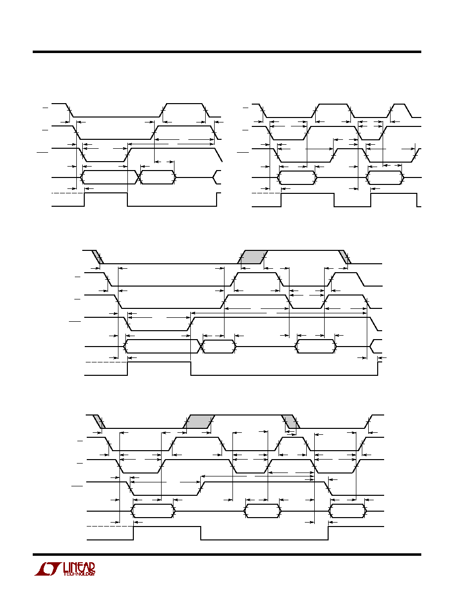
Slow Memory Mode, Parallel Read Timing Diagram
ROM Mode, Parallel Read Timing Diagram
Slow Memory Mode, Two Byte Read Timing Diagram
BUSY
DATA
TRACK
OLD DATA
DB11 TO DB0
NEW DATA
DB11 TO DB0
t
1
HOLD
LTC1282 · TC01
CS
RD
t
5
t
1
t
10
t
11
t
2
t
CONV
t
7
t
6
t
3
t
12
t
1
OLD DATA
DB11 TO DB0
NEW DATA
DB11 TO DB0
DATA
TRACK
HOLD
CS
RD
BUSY
LTC1282 · TC02
t
5
t
1
t
5
t
4
t
2
t
CONV
t
11
t
2
t
CONV
t
3
t
7
t
3
t
7
t
12
t
12
t
4
ROM Mode, Two Byte Read Timing Diagram
CS
RD
BUSY
DATA
TRACK
HOLD
HBEN
OLD DATA
DB7 TO DB0
NEW DATA
DB7 TO DB0
NEW DATA
DB11 TO DB8
LTC1282 · TC03
t
7
t
8
t
1
t
2
t
3
t
12
t
6
t
7
t
3
t
CONV
t
9
t
8
t
9
t
5
t
4
t
1
t
5
t
10
t
10
t
11
t
12
CS
RD
BUSY
DATA
TRACK
HOLD
HBEN
OLD DATA
DB7 TO DB0
NEW DATA
DB7 TO DB0
NEW DATA
DB11 TO DB8
LTC1282 · TC04
t
8
t
9
t
8
t
9
t
8
t
9
t
1
t
4
t
5
t
1
t
4
t
5
t
1
t
5
t
4
t
2
t
CONV
t
11
t
10
t
2
t
7
t
3
t
7
t
3
t
7
t
3
t
12
t
12