 | –≠–ª–µ–∫—Ç—Ä–æ–Ω–Ω—ã–π –∫–æ–º–ø–æ–Ω–µ–Ω—Ç: LTC1283CN | –°–∫–∞—á–∞—Ç—å:  PDF PDF  ZIP ZIP |
1
LTC1283
3V Single Chip 10-Bit Data
Acquisition System
D
U
ESCRIPTIO
S
FEATURE
s
Single Supply 3.3V or
±
3.3V Operation
s
Software Programmable Features:
Unipolar/Bipolar Conversions
4 Differential/8 Single-Ended Inputs
MSB- or LSB-First Data Sequence
Variable Data Word Length
s
Built-In Sample-and-Hold
s
Direct 4-Wire Interface to Most MPU Serial Ports
and all MPU Parallel Ports
s
15kHz Maximum Throughput Rate
U
A
O
PPLICATI
TYPICAL
Linearity Plot
KEY SPECIFICATIO S
U
s
Minimum Guaranteed Supply Voltage: 3V
s
Resolution: 10 Bits
s
Offset Error:
±
0.5LSB Max
s
Linearity Error:
±
0.5LSB Max
s
Gain Error (LTC1283A):
±
1LSB Max
s
Conversion Time: 44
µ
s
s
Supply Current: 350
µ
A Max, 150
µ
A Typ
OUTPUT CODE
0
ERROR (LSBs)
0
0.5
1024
LTC1283 ∑ TA02
≠0.5
≠ 1.0
512
1.0
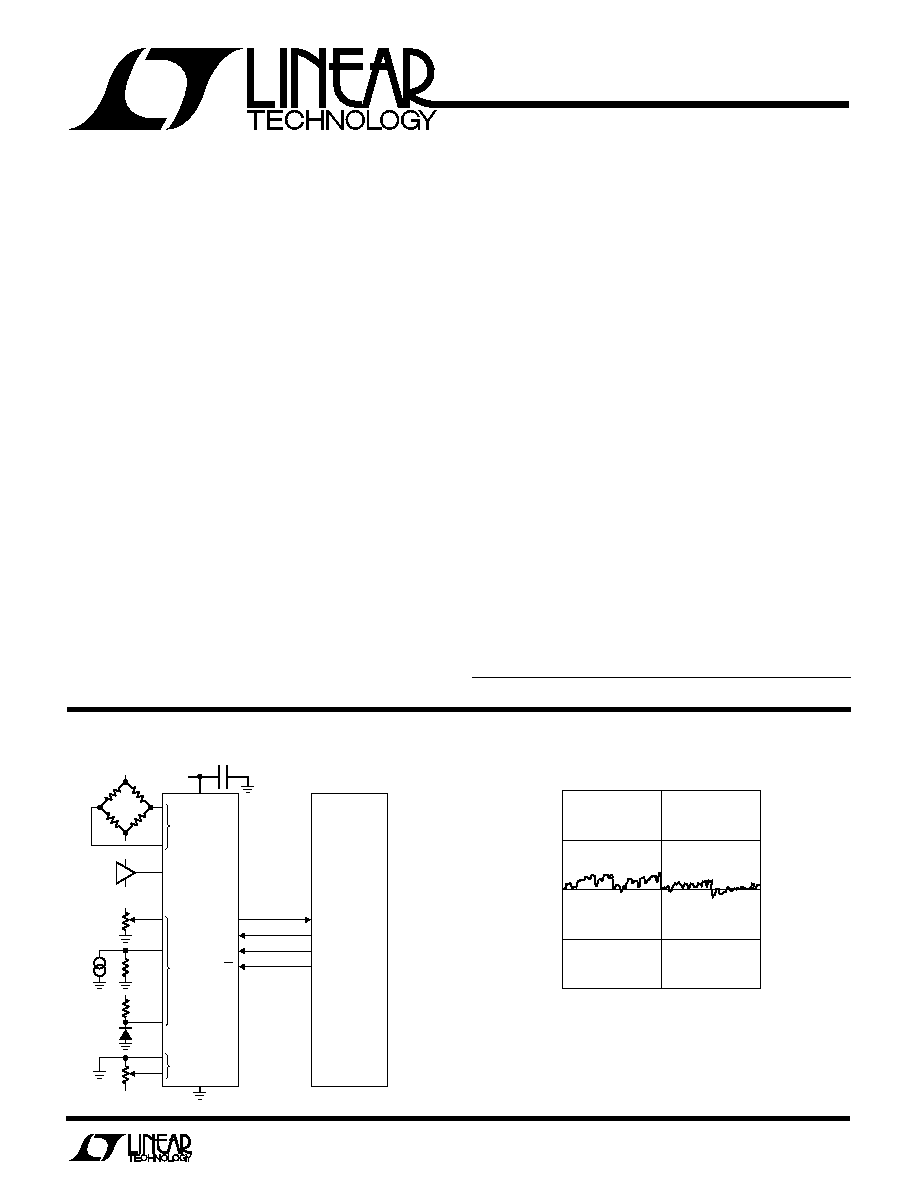
The LTC1283 is a 3V data acquisition component which
contains a serial I/O successive approximation A/D con-
verter. It uses LTCMOS
TM
switched capacitor technology
to perform either 10-bit unipolar, or 9-bit plus sign bipolar
A/D conversions. The 8-channel input multiplexer can be
configured for either single-ended or differential inputs (or
combinations thereof). An on-chip sample-and-hold is
included for all single-ended input channels.
The serial I/O is designed to be compatible with industry-
standard full-duplex serial interfaces. It allows either MSB-
or LSB-first data and automatically provides 2's comple-
ment output coding in the bipolar mode. The output data
word can be programmed for a length of 8-, 10-, 12-, or
16-bit. This allows easy interface to shift registers and a
variety of processors.
Both the LTC1283A and LTC1283 are specified with offset
and linearity errors less than
±
0.5LSB. The LTC1283A has
a gain error limit of
±
1LSB. The 1283 is specified with a
gain error limit of
±
2LSB for applications where gain is
adjustable or less critcial.
LTCMOS is a trademark of Linear Technology Corp.
DIFFERENTIAL
INPUT
LTC1283
3V
BIPOLAR
INPUT
≠3V
3V
T
≠3V
UNIPOLAR
INPUTS
(+)
(≠)
≠UNIPOLAR
INPUT
MPU
(e.g., 83CL410)
P1.1
P1.2
P1.3
P1.4
SERIAL DATA LINK
FOR 83CL410 CODE SEE
APPLICATIONS INFORMATION SECTION
LTC1283 ∑ TA01
D
OUT
D
IN
SCLK
CS
4.7
µ
F
3V

2
LTC1283
A
U
G
W
A
W
U
W
A
R
BSOLUTE
XI
TI
S
SYMBOL
PARAMETER
CONDITIONS
MIN
TYP
MAX
UNITS
V
CC
Positive Supply Voltage
V
≠
= 0V
3.0
3.6
V
V
≠
Negative Supply Voltage
V
CC
= 3.3V
≠ 3.6
0
V
f
SCLK
Shift Clock Frequency
V
CC
= 3V
0
500
kHz
f
ACLK
A/D Clock Frequency
V
CC
= 3V
T
A
25
∞
C
0.01
1.00
MHz
T
A
70
∞
C
0.05
1.00
MHz
t
CYC
Total Cycle Time
See Operating Sequence
10 SCLK +
Cycles
48 ACLK
t
hCS
Hold Time, CS Low After Last SCLK
V
CC
= 3V
0
ns
t
hDI
Hold Time, D
IN
After SCLK
V
CC
= 3V
200
ns
t
suCS
Setup Time CS
Before Clocking in First Address Bit (Note 8)
V
CC
= 3V
2 ACLK Cycles
+ 1
µ
s
t
suDI
Setup Time, D
IN
Stable Before SCLK
V
CC
= 3V
400
ns
t
WHACLK
ACLK High Time
V
CC
= 3V
250
ns
t
WLACLK
ACLK Low Time
V
CC
= 3V
400
ns
t
WHCS
CS High Time During Conversion
V
CC
= 3V
44
ACLK
Cycles
LTC1283/LTC1283A
Supply Voltage (V
CC
) to GND or V
≠
......................... 12V
Voltage
Analog and Reference
Inputs ................................. (V
≠
) ≠0.3V to V
CC
+ 0.3V
Digital Inputs ......................................... ≠0.3V to 12V
Digital Outputs ........................... ≠0.3V to V
CC
+ 0.3V
(Notes 1 and 2)
Negative Supply Voltage (V≠) ..................... ≠6V to GND
Power Dissipation .............................................. 500mW
Operating Temperature
LTC1283AC, LTC1283C ......................... 0
∞
C to 70
∞
C
Storage Temperature Range ................. ≠ 65
∞
C to 150
∞
C
Lead Temperature (Soldering, 10 sec)................. 300
∞
C
RECO E DED OPERATI G CO DITIO S
W
U
W
U
U
U
W
U
U
PACKAGE/ORDER I FOR ATIO
ORDER PART
NUMBER
LTC1283ACN
LTC1283CN
ORDER PART
NUMBER
LTC1283ACS
LTC1283CS
1
2
3
4
5
6
7
8
9
10
TOP VIEW
N PACKAGE
20-LEAD PLASTIC DIP
20
19
18
17
16
15
14
13
12
11
CH0
CH1
CH2
CH3
CH4
CH5
CH6
CH7
COM
DGND
V
CC
ACLK
SCLK
D
IN
D
OUT
CS
REF
+
REF
≠
V
≠
AGND
T
J MAX
= 150
∞
C,
JA
= 100
∞
C/W
1
2
3
4
5
6
7
8
9
10
TOP VIEW
S PACKAGE
20-LEAD PLASTIC SOL
20
19
18
17
16
15
14
13
12
11
CH0
CH1
CH2
CH3
CH4
CH5
CH6
CH7
COM
DGND
V
CC
ACLK
SCLK
D
IN
D
OUT
CS
REF
+
REF
≠
V
≠
AGND
T
J MAX
= 150
∞
C,
JA
= 130
∞
C/W
Consult factory for Industrial and Military grade parts
3
LTC1283
LTC1283A
LTC1283
PARAMETER
CONDITIONS
MIN
TYP
MAX
MIN
TYP
MAX
UNITS
Offset Error
(Note 4)
q
±
0.5
±
0.5
LSB
Linearity Error
(Notes 4 and 5)
q
±
0.5
±
0.5
LSB
Gain Error
(Note 4)
q
±
1.0
±
2.0
LSB
Minimum Resolution for Which No
q
10
10
Bits
Missing Codes are Guaranteed
Reference Input Resistance
10
10
k
Analog and REF Input Range
(Note 6)
V
On Channel Leakage Current
On Channel = 3V
q
1
1
µ
A
(Note 7)
Off Channel = 0V
On Channel = 0V
q
≠ 1
≠ 1
µ
A
Off Channel = 3V
Off Channel Leakage Current
On Channel = 3V
q
≠ 1
≠ 1
µ
A
(Note 7)
Off Channel = 0V
On Channel = 0V
q
1
1
µ
A
Off Channel = 3V
(V
≠
) ≠ 0.05V to V
CC
+ 0.05V
AC CHARACTERISTICS
CO VERTER A D ULTIPLEXER CHARACTERISTICS
U
U W
(Note 3)
(Note 3)
ELECTRICAL C
C
HARA TER STICS
DIGITAL A D
U
I
DC
SYMBOL
PARAMETER
CONDITIONS
MIN
TYP
MAX
UNITS
t
ACC
Delay Time From CS
to D
OUT
Data Valid
(Note 8)
2
ACLK Cycles
t
SMPL
Analog Input Sample Time
See Operating Sequence
5
SCLK Cycles
t
CONV
Conversion Time
See Operating Sequence
44
ACLK Cycles
t
dDO
Delay Time, SCLK
to D
OUT
Data Valid
See Test Circuts
q
400
900
ns
t
dis
Delay Time, CS
to D
OUT
Hi-Z
See Test Circuits
q
240
500
ns
t
en
Delay Time, 2nd CLK
to D
OUT
Enabled
See Test Circuits
q
300
800
ns
t
hDO
Time Output Data Remains Valid After SCLK
75
ns
t
f
D
OUT
Fall Time
See Test Circuits
q
90
300
ns
t
r
D
OUT
Rise Time
See Test Circuits
q
80
300
ns
C
IN
Input Capacitance
Analog Inputs On Channel
65
pF
Off Channel
5
pF
Digital Inputs
5
pF
LTC1283/LTC1283A
SYMBOL
PARAMETER
CONDITIONS
MIN
TYP
MAX
UNITS
V
IH
High Level Input Voltage
V
CC
= 3.6V
q
1.7
V
V
IL
Low Level Input Voltage
V
CC
= 3V
q
0.45
V
I
IH
High Level Input Current
V
IN
= V
CC
q
2.5
µ
A
I
IL
Low Level Input Current
V
IN
= 0V
q
≠ 2.5
µ
A
V
OH
High Level Output Voltage
V
CC
= 3V, I
O
= ≠ 20
µ
A
2.6
2.8
V
I
O
= ≠ 200
µ
A
q
2.0
V
V
OL
Low Level Output Voltage
V
CC
= 3V, I
O
= 20
µ
A
0.05
V
I
O
= 400
µ
A
q
0.10
0.30
V
LTC1283/LTC1283A
(Note 3)
4
LTC1283
ELECTRICAL C
C
HARA TER STICS
DIGITAL A D
U
I
DC
SYMBOL
PARAMETER
CONDITIONS
MIN
TYP
MAX
UNITS
I
OZ
Hi-Z Output Leakage
V
OUT
= V
CC
, CS High
q
3
µ
A
V
OUT
= 0V, CS High
q
≠ 3
µ
A
I
SOURCE
Output Source Current
V
OUT
= 0V
≠ 4.5
mA
I
SINK
Output Sink Current
V
OUT
= V
CC
4.5
mA
I
CC
Positive Supply Current
CS High, REF
+
Open
q
150
350
µ
A
I
REF
Reference Current
V
REF
= 2.5V
q
250
500
µ
A
I
≠
Negative Supply Current
CS High, V
≠
= ≠ 3V
q
≠1
≠ 50
µ
A
LTC1283/LTC1283A
(Note 3)
The
q
denotes specifications which apply over the operating temperature
range; all other limits and typicals T
A
= 25
∞
C.
Note 1: Absolute maximum ratings are those values beyond which the life
of a device may be impaired.
Note 2: All voltage values are with respect to ground with DGND, AGND
and REF
≠
wired together (unless otherwise noted).
Note 3: V
CC
= 3V, V
REF
+
= 2.5V, V
REF
≠
= 0V, V
≠
= 0V for unipolar mode
and ≠ 3V for bipolar mode, ACLK = 1MHz, SCLK = 0.25MHz unless
otherwise specified.
Note 4: These specifications apply for both unipolar and bipolar modes. In
bipolar mode, one LSB is equal to the bipolar input span (2V
REF
) divided
by 1024. For example, when V
REF
= 2.5V, 1LSB (bipolar) = 2(2.5V)/1024 =
4.88mV.
Note 5: Linearity error is the deviation from ideal of the slope between the
two end points of the transfer curve.
Note 6: Two on-chip diodes are tied to each reference and analog input
which will conduct for reference or analog input voltages one diode drop
below V
≠
or one diode drop above V
CC
. Be careful during testing at low
V
CC
levels, as high level reference or analog inputs can cause this input
diode to conduct, especially at elevated temperatures, and cause errors for
inputs near full scale. This spec allows 50mV forward bias of either diode.
This means that as long as the reference or analog input does not exceed
the supply voltage by more than 50mV, the output code will be correct.
Note 7: Channel leakage current is measured after the channel selection.
Note 8: To minimize errors caused by noise at the chip select input, the
internal circuitry waits for two ACLK falling edges after a chip select falling
edge is detected before responding to control input signals. Therefore, no
attempt should be made to clock an address in or data out until the
minimum chip select setup time has elapsed.
C
C
HARA TERISTICS
U
W
A
TYPICAL PERFOR
CE
Supply Current vs Temperature
Reference Current vs Temperature
AMBIENT TEMPERATURE (∞C)
≠50
0
SUPPLY CURRENT, I
CC
(
µ
A)
100
250
0
50
75
LTC1283 ∑ G01
50
200
150
≠25
25
100
125
REF
+
OPEN
ACLK = 500kHz
V
CC
= CS = 3V
REFERENCE VOLTAGE (V)
0
6
8
10
2.0
LTC1283 ∑ G03
4
2
0
0.5
1.0
1.5
2.5
5
7
9
3
1
V
CC
= 3V
ACLK = 500kHz
OFFSET ERROR (LSBs =
1
1024
◊
V
REF
)
Unadjusted Offset Error
vs Reference Voltage
TEMPERATURE (∞C)
≠50
0
I
REF
(
µ
A)
200
500
0
50
75
LTC1283 ∑ G02
100
400
300
≠25
25
100
125
V
CC
= 3V
V
REF
= 2.5V
5
LTC1283
C
C
HARA TERISTICS
U
W
A
TYPICAL PERFOR
CE
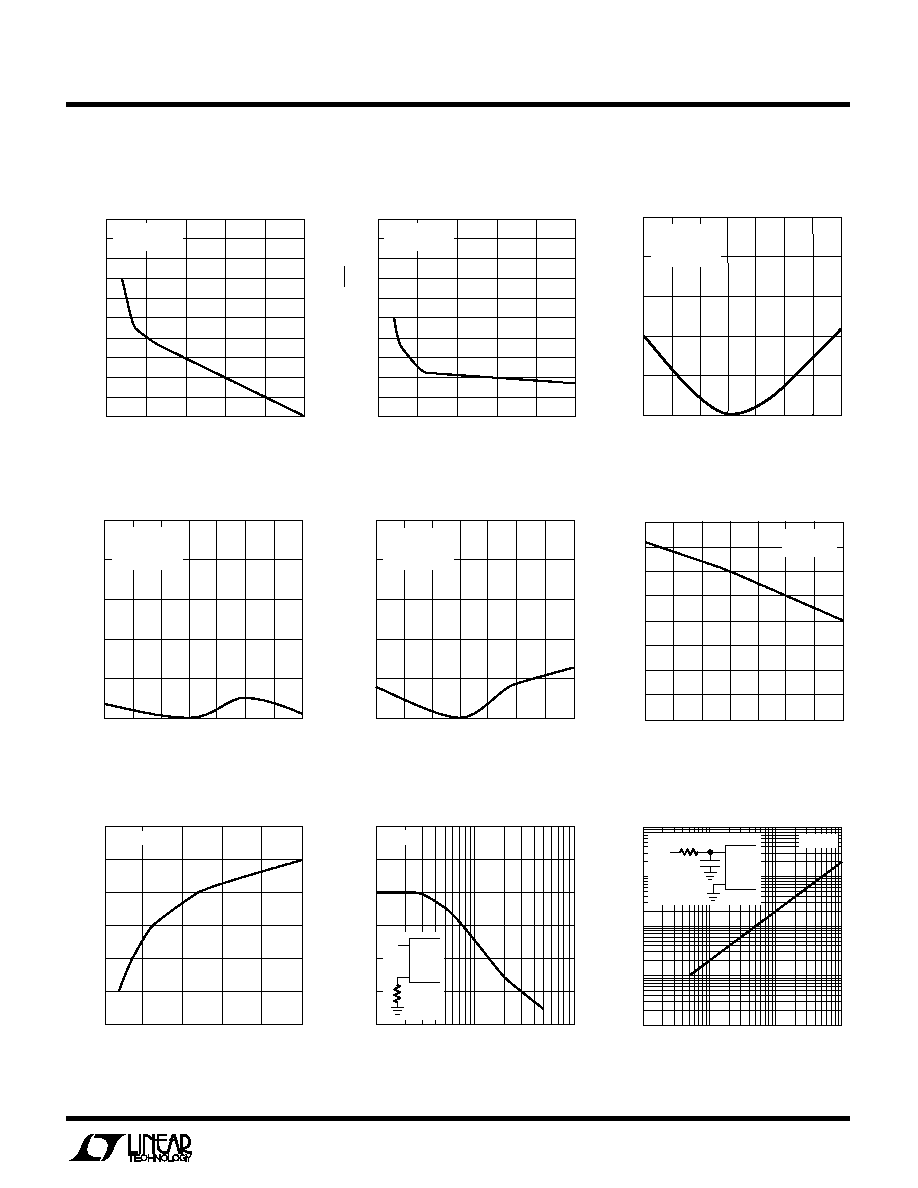
Linearity Error
vs Reference Voltage
Change in Linearity Error
vs Temperature
Maximum Conversion Clock Rate
vs Temperature
Change in Gain Error
vs Temperature
Maximum Conversion Clock Rate
vs Source Resistance
Maximum Conversion Clock Rate
vs Reference Voltage
Change in Full-Scale Error
vs Reference Voltage
Change in Offset Error
vs Temperature
AMBIENT TEMPERATURE (∞C)
≠50
MAXIMUM ACLK FREQUENCY* (MHz)
1.75
25
LTC1283 ∑ G09
1.0
0.5
≠25
0
50
0.25
0
2.0
1.5
1.25
0.75
75
100
125
V
CC
= 3V
V
REF
= 2.5V
R
SOURCE
(k
)
1
0
MAXIMUM ACLK FREQUENCY* (kHz)
250
500
750
1000
1500
10
100
LTC1283 ∑ G11
1250
V
CC
= 3V
+ INPUT
≠ INPUT
R
SOURCE
≠
V
IN
REFERENCE VOLTAGE (V)
0
CHANGE IN GAIN ERROR (LSB)
0.6
0.8
1.0
2.0
LTC1283 ∑ G04
0.4
0.2
0
0.5
1.0
1.5
2.5
0.5
0.7
0.9
0.3
0.1
V
CC
= 3V
ACLK = 500kHz
REFERENCE VOLTAGE (V)
0
0.6
0.8
1.0
2.0
LTC1283 ∑ G05
0.4
0.2
0
0.5
1.0
1.5
2.5
0.5
0.7
0.9
0.3
0.1
V
CC
= 3V
ACLK = 500kHz
LINEARITY ERROR (LSBs =
1
1024
◊
V
REF
)
AMBIENT TEMPERATURE (∞C)
≠50
0
MAGNITUDE OF OFFSET CHANGE,
OFFSET
(LSB)
0.2
0.5
0
50
75
LTC1283 ∑ G06
0.1
0.4
0.3
≠25
25
100
125
V
CC
= 3V
V
REF
= 2.5V
ACLK = 500kHz
AMBIENT TEMPERATURE (∞C)
≠50
0
MAGNITUDE OF LINEARITY CHANGE,
LINEARITY
(LSB)
0.2
0.5
0
50
75
LTC1283 ∑ G07
0.1
0.4
0.3
≠25
25
100
125
V
CC
= 3V
V
REF
= 2.5V
ACLK = 500kHz
TEMPERATURE (∞C)
≠50
0
MAGNITUDE OF GAIN CHANGE,
GAIN
(LSB)
0.2
0.5
0
50
75
LTC1283 ∑ G08
0.1
0.4
0.3
≠25
25
100
125
V
CC
= 3V
V
REF
= 2.5V
ACLK = 500kHz
REFERENCE VOLTAGE (V)
0
0
MAXIMUM ACLK FREQUENCY* (kHz)
250
500
750
1000
1250
1500
0.5
1.0
1.5
2.0
LTC1283 ∑ G10
2.5
V
CC
= 3V
*Maximum ACLK frequency represents the ACLK frequency at which a 0.1LSB shift in the error at
any code transition from its 100kHz value is first detected.
**Maximum R
FILTER
represents the filter resistor value at which a 0.1LSB change in full-scale error
from its value at R
FILTER
= 0 is first detected.
Maximum Filter Resistor
vs Cycle Time
CYCLE TIME (
µ
s)
100
MAXIMUM R
FILTER
** (
)
1k
10k
100k
10
1000
10000
LTC1283 ∑ G12
10
100
+
≠
V
IN
R
FILTER
C
FILTER
1
µ
F
V
CC
= 3V