 | –≠–ª–µ–∫—Ç—Ä–æ–Ω–Ω—ã–π –∫–æ–º–ø–æ–Ω–µ–Ω—Ç: LTC1286C | –°–∫–∞—á–∞—Ç—å:  PDF PDF  ZIP ZIP |
1
LTC1286/LTC1298
Micropower Sampling
12-Bit A/D Converters In
S0-8 Packages
s
12-Bit Resolution
s
8-Pin SOIC Plastic Package
s
Low Cost
s
Low Supply Current: 250
µ
A Typ.
s
Auto Shutdown to 1nA Typ.
s
Guaranteed
±
3/4LSB Max DNL
s
Single Supply 5V to 9V Operation
s
On-Chip Sample-and-Hold
s
60
µ
s Conversion Time
s
Sampling Rates:
12.5 ksps (LTC1286)
11.1 ksps (LTC1298)
s
I/O Compatible with SPI, Microwire, etc.
s
Differential Inputs (LTC1286)
s
2-Channel MUX (LTC1298)
s
3V Versions Available: LTC1285/LTC1288
The LTC1286/LTC1298 are micropower, 12-bit, succes-
sive approximation sampling A/D converters. They typi-
cally draw only 250
µ
A of supply current when converting
and automatically power down to a typical supply current
of 1nA whenever they are not performing conversions.
They are packaged in 8-pin SO packages and operate on
5V to 9V supplies. These 12-bit, switched-capacitor, suc-
cessive approximation ADCs include sample-and-holds.
The LTC1286 has a single differential analog input. The
LTC1298 offers a software selectable 2-channel MUX.
On-chip serial ports allow efficient data transfer to a wide
range of microprocessors and microcontrollers over three
wires. This, coupled with micropower consumption, makes
remote location possible and facilitates transmitting data
through isolation barriers.
These circuits can be used in ratiometric applications or
with an external reference. The high impedance analog
inputs and the ability to operate with reduced spans (to
1.5V full scale) allow direct connection to sensors and
transducers in many applications, eliminating the need for
gain stages.
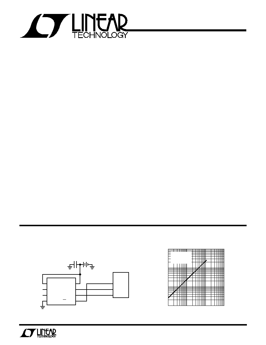
5V
4.7
µ
F
ANALOG INPUT
≠IN
GND
V
CC
CLK
D
OUT
V
REF
LTC1286
MPU
(e.g., 8051)
P1.4
P1.3
P1.2
+IN
0V TO 5V RANGE
LTC1286/98 ∑ TA01
CS/SHDN
6
5
8
7
3
4
1
2
SERIAL DATA LINK
s
Battery-Operated Systems
s
Remote Data Acquisition
s
Battery Monitoring
s
Handheld Terminal Interface
s
Temperature Measurement
s
Isolated Data Acquisition
SAMPLE FREQUENCY (Hz)
0.1k
1
SUPPLY CURRENT (
µ
A)
10
100
1000
1k
10k
100k
LTC1286/98 ∑ TA02
T
A
= 25∞C
V
CC
= V
REF
= 5V
f
CLK
= 200kHz
DESCRIPTIO
N
U
25
µ
W, S0-8 Package, 12-Bit ADC
Samples at 200Hz and Runs Off a 5V Supply
Supply Current vs Sample Rate
FEATURES
APPLICATIO
N
S
U
TYPICAL APPLICATIO
N
S
N
U
2
LTC1286/LTC1298
1298C
1298I
ORDER PART
NUMBER
LTC1286CN8
LTC1286IN8
T
JMAX
= 150
∞
C,
JA
= 130
∞
C/W
T
JMAX
= 150
∞
C,
JA
= 175
∞
C/W
ORDER PART
NUMBER
PACKAGE/ORDER I
N
FOR
M
ATIO
N
W
U
U
ABSOLUTE
M
AXI
M
U
M
RATINGS
W
W
W
(Notes 1 and 2)
Power Dissipation .............................................. 500mW
Operating Temperature Range
LTC1286C/LTC1298C ............................. 0
∞
C to 70
∞
C
LTC1286I/LTC1298I ........................... ≠40
∞
C to 85
∞
C
Storage Temperature Range ................. ≠ 65
∞
C to 150
∞
C
Lead Temperature (Soldering, 10 sec.) ................ 300
∞
C
Supply Voltage (V
CC
) to GND ................................... 12V
Voltage
Analog and Reference ................ ≠0.3V to V
CC
+ 0.3V
Digital Inputs ......................................... ≠0.3V to 12V
Digital Output ............................. ≠0.3V to V
CC
+ 0.3V
PART MARKING
1286C
1286I
ORDER PART
NUMBER
LTC1298CN8
LTC1298IN8
ORDER PART
NUMBER
PART MARKING
LTC1298CS8
LTC1298IS8
LTC1286CS8
LTC1286IS8
SYMBOL
PARAMETER
CONDITIONS
MIN
TYP
MAX
UNITS
V
CC
Supply Voltage (Note 3)
LTC1286
4.5
9.0
V
LTC1298
4.5
5.5
V
f
CLK
Clock Frequency
V
CC
= 5V
(Note 4)
200
kHz
t
CYC
Total Cycle Time
LTC1286, f
CLK
= 200kHz
80
µ
s
LTC1298, f
CLK
= 200kHz
90
µ
s
t
hDI
Hold Time, D
IN
After CLK
V
CC
= 5V
150
ns
t
suCS
Setup Time CS
Before First CLK
(See Operating Sequence)
LTC1286, V
CC
= 5V
2
µ
s
LTC1298, V
CC
= 5V
2
µ
s
t
suDI
Setup Time, D
IN
Stable Before CLK
V
CC
= 5V
400
ns
t
WHCLK
CLK High Time
V
CC
= 5V
2
µ
s
t
WLCLK
CLK Low Time
V
CC
= 5V
2
µ
s
t
WHCS
CS High Time Between Data Transfer Cycles
V
CC
= 5V
2
µ
s
t
WLCS
CS Low Time During Data Transfer
LTC1286, f
CLK
= 200kHz
75
µ
s
LTC1298, f
CLK
= 200kHz
85
µ
s
RECO
M
E
N
DED OPERATI
N
G CO
N
DITIO
N
S
U
U
U
U
W
W
Consult factory for military grade parts.
1
2
3
4
8
7
6
5
TOP VIEW
V
REF
+IN
≠IN
GND
V
CC
CLK
D
OUT
N8 PACKAGE
8-LEAD PLASTIC DIP
CS/SHDN
1
2
3
4
8
7
6
5
TOP VIEW
CH0
CH1
GND
V
CC
(V
REF
)
CLK
D
OUT
D
IN
N8 PACKAGE
8-LEAD PLASTIC DIP
CS/SHDN
1
2
3
4
8
7
6
5
TOP VIEW
V
CC
(V
REF
)
CLK
D
OUT
D
IN
CH0
CH1
GND
S8 PACKAGE
8-LEAD PLASTIC SOIC
CS/SHDN
1
2
3
4
8
7
6
5
TOP VIEW
V
CC
CLK
D
OUT
V
REF
+IN
≠IN
GND
S8 PACKAGE
8-LEAD PLASTIC SOIC
CS/SHDN
T
JMAX
= 150
∞
C,
JA
= 130
∞
C/W
T
JMAX
= 150
∞
C,
JA
= 175
∞
C/W
3
LTC1286/LTC1298
SYMBOL
PARAMETER
CONDITIONS
MIN
TYP
MAX
UNITS
S/(N +D)
Signal-to-Noise Plus Distortion Ratio
1kHz/7kHz Input Signal
71/68
dB
THD
Total Harmonic Distortion (Up to 5th Harmonic)
1kHz/7kHz Input Signal
≠ 84/≠80
dB
SFDR
Spurious-Free Dynamic Range
1kHz/7kHz Input Signal
90/86
dB
Peak Harmonic or Spurious Noise
1kHz/7kHz Input Signal
≠ 90/≠86
dB
f
SMPL
= 12.5kHz (LTC1286), f
SMPL
= 11.1kHz (LTC1298) (Note 5)
CO
N
VERTER A
N
D
M
ULTIPLEXER CHARACTERISTICS
U
W
U
(Note 5)
DY
N
A
M
IC ACCURACY
U
W
SYMBOL
PARAMETER
CONDITIONS
MIN
TYP
MAX
UNITS
V
IH
High Level Input Voltage
V
CC
= 5.25V
q
2
V
V
IL
Low Level Input Voltage
V
CC
= 4.75V
q
0.8
V
I
IH
High Level Input Current
V
IN
= V
CC
q
2.5
µ
A
I
IL
Low Level Input Current
V
IN
= 0V
q
≠ 2.5
µ
A
V
OH
High Level Output Voltage
V
CC
= 4.75V, I
O
= 10
µ
A
q
4.0
4.64
V
V
CC
= 4.75V, I
O
= 360
µ
A
q
2.4
4.62
V
V
OL
Low Level Output Voltage
V
CC
= 4.75V, I
O
= 1.6mA
q
0.4
V
I
OZ
Hi-Z Output Leakage
CS = High
q
±
3
µ
A
I
SOURCE
Output Source Current
V
OUT
= 0V
≠ 25
mA
I
SINK
Output Sink Current
V
OUT
= V
CC
45
mA
R
REF
Reference Input Resistance
CS = V
CC
5000
M
(LTC1286)
CS = GND
55
k
I
REF
Reference Current (LTC1286)
CS = V
CC
q
0.001
2.5
µ
A
t
CYC
640
µ
s, f
CLK
25kHz
q
90
140
µ
A
t
CYC
= 80
µ
s, f
CLK
= 200kHz
q
90
140
µ
A
I
CC
Supply Current
CS = V
CC
q
0.001
±
3.0
µ
A
LTC1286, t
CYC
640
µ
s, f
CLK
25kHz
q
200
400
µ
A
LTC1286, t
CYC
= 80
µ
s, f
CLK
= 200kHz
q
250
500
µ
A
LTC1298, t
CYC
720
µ
s, f
CLK
25kHz
q
290
490
µ
A
LTC1298, t
CYC
= 90
µ
s, f
CLK
= 200kHz
q
340
640
µ
A
(Note 5)
1.5V to V
CC
+ 0.05V
1.5V to 5.55V
≠0.05V to V
CC
+ 0.05V
LTC1286
LTC1298
PARAMETER
CONDITIONS
MIN
TYP
MAX
MIN
TYP
MAX
UNITS
Resolution (No Missing Codes)
q
12
12
Bits
Integral Linearity Error
(Note 6)
q
±
3/4
±
2
±
3/4
±
2
LSB
Differential Linearity Error
q
±
1/4
±
3/4
±
1/4
±
3/4
LSB
Offset Error
q
3/4
±
3
3/4
±
3
LSB
Gain Error
q
±
2
±
8
±
2
±
8
LSB
Analog Input Range
(Note 7 and 8)
q
V
REF Input Range (LTC1286)
4.5
V
CC
5.5V
V
(Notes 7, 8, and 9)
5.5V < V
CC
9V
V
Analog Input Leakage Current (Note 10)
q
±
1
±
1
µ
A
DIGITAL A
N
D DC ELECTRICAL CHARACTERISTICS
U
4
LTC1286/LTC1298
SYMBOL
PARAMETER
CONDITIONS
MIN
TYP
MAX
UNITS
t
SMPL
Analog Input Sample Time
See Operating Sequence
1.5
CLK Cycles
f
SMPL (MAX)
Maximum Sampling Frequency
LTC1286
q
12.5
kHz
LTC1298
q
11.1
kHz
t
CONV
Conversion Time
See Operating Sequence
12
CLK Cycles
t
dDO
Delay Time, CLK
to D
OUT
Data Valid
See Test Circuits
q
250
600
ns
t
dis
Delay Time, CS
to D
OUT
Hi-Z
See Test Circuits
q
135
300
ns
t
en
Delay Time, CLK
to D
OUT
Enable
See Test Circuits
q
75
200
ns
t
hDO
Time Output Data Remains Valid After CLK
C
LOAD
= 100pF
230
ns
t
f
D
OUT
Fall Time
See Test Circuits
q
20
75
ns
t
r
D
OUT
Rise Time
See Test Circuits
q
20
75
ns
C
IN
Input Capacitance
Analog Inputs, On Channel
20
pF
Analog Inputs, Off Channel
5
pF
Digital Input
5
pF
AC CHARACTERISTICS
(Note 5)
The
q
denotes specifications which apply over the full operating
temperature range.
Note 1: Absolute maximum ratings are those values beyond which the life
of a device may be impaired.
Note 2: All voltage values are with respect to GND.
Note 3: These devices are specified at 5V. For 3V specified devices, see
LTC1285 and LTC1288.
Note 4: Increased leakage currents at elevated temperatures cause the S/H
to droop, therefore it is recommended that f
CLK
120kHz at 85
∞
C, f
CLK
75kHz at 70
∞
and f
CLK
1kHz at 25
∞
C.
Note 5: V
CC
= 5V, V
REF
= 5V and CLK = 200kHz unless otherwise specified.
Note 6: Linearity error is specified between the actual end points of the
A/D transfer curve.
Note 7: Two on-chip diodes are tied to each reference and analog input
which will conduct for reference or analog input voltages one diode drop
below GND or one diode drop above V
CC
. This spec allows 50mV forward
bias of either diode for 4.5V
V
CC
5.5V. This means that as long as the
reference or analog input does not exceed the supply voltage by more than
50mV the output code will be correct. To achieve an absolute 0V to 5V
input voltage range will therefore require a minimum supply voltage of
4.950V over initial tolerance, temperature variations and loading. For 5.5V
< V
CC
9V, reference and analog input range cannot exceed 5.55V. If
reference and analog input range are greater than 5.55V, the output code
will not be guaranteed to be correct.
Note 8: The supply voltage range for the LTC1286 is from 4.5V to 9V, but
the supply voltage range for the LTC1298 is only from 4.5V to 5.5V.
Note 9: Recommended operating conditions
Note 10: Channel leakage current is measured after the channel selection.
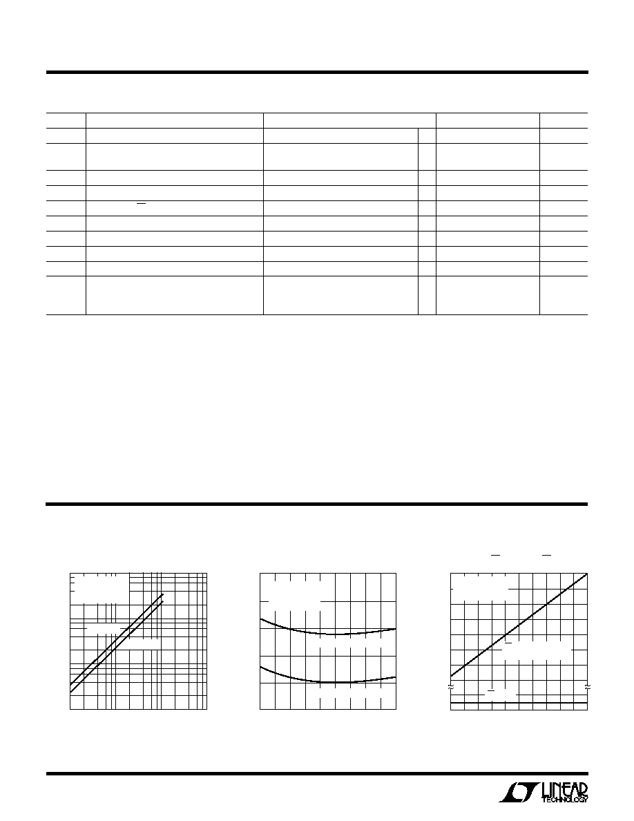
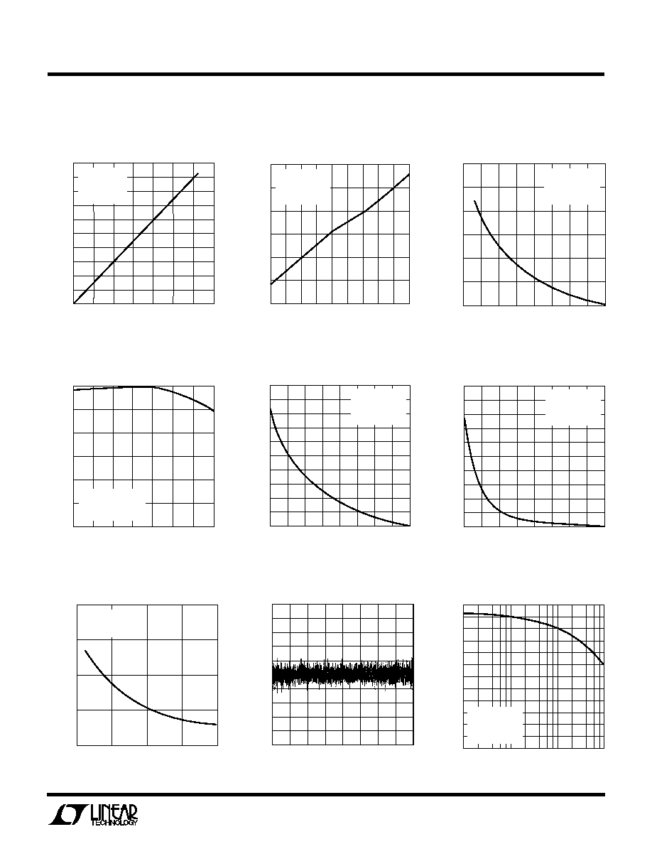
TYPICAL PERFOR
M
A
N
CE CHARACTERISTICS
U
W
Shutdown Supply Current vs Clock
Rate with CS High and CS Low
Supply Current vs Sample Rate
SAMPLE RATE (kHz)
0.1k
1
10
100
1000
1k
10k
100k
LT1286/98 G03
SUPPLY CURRENT (µA)
T
A
= 25∞C
V
CC
= V
REF
= 5V
f
CLK
= 200kHz
LTC1286
LTC1298
Supply Current vs Temperature
TEMPERATURE (∞C)
≠55
200
SUPPLY CURRENT (µA)
250
350
400
450
≠15
25
45
125
LT1286/98 G04
300
≠35
5
65
85 105
T
A
= 25∞C
V
CC
= V
REF
= 5V
f
CLK
= 200kHz
LTC1298 f
SMPL
=11.1kHz
LTC1286 f
SMPL
=12.5kHz
FREQUENCY (kHz)
1
0.002
SUPPLY CURRENT (µA)
5
1
0
15
20
25
35
20
100
140
LT1286/98 G01
10
30
80
180 200
40 60
120
160
CS = 0
(AFTER CONVERSION)
T
A
= 25∞C
V
CC
= V
REF
= 5V
CS = V
CC
5
LTC1286/LTC1298
TYPICAL PERFOR
M
A
N
CE CHARACTERISTICS
U
W
0
≠ 0 .05
≠ 0 .15
≠ 0 .2
≠ .25
≠ 0 .3
≠ 0 .5
≠ 0 .35
≠ 0 .1
≠ 0 .4
≠ 0 .45
REFERENCE VOLTAGE (V)
1
CHANGE IN LINEARITY (LSB)
2
3
4
5
LT1286/98 G10
1.5
2.5
3.5
4.5
T
A
= 25∞C
V
CC
= 5V
f
CLK
= 200kHz
f
SMPL
= 12.5kHz
FREQUENCY (kHz)
0
0
REFERENCE CURRENT (
µ
A)
10
30
40
50
100
70
4
8
10
LT1286/98 G06
20
80
90
60
2
6
12
14
T
A
= 25∞C
V
CC
= 5V
V
REF
= 5V
f
CLK
= 200kHz
TEMPERATURE (∞C)
≠55
92
REFERENCE CURRENT (µA)
92.5
93.5
94
94.5
≠15
25
45
125
LT1286/98 G07
93
≠35
5
65
85 105
95
V
CC
= V
REF
= 5V
f
SMPL
= 12.5kHz
f
CLK
= 200kHz
T
A
= 25∞C
Reference Current vs Temperature
REFERENCE VOLTAGE (V)
1
0
CHANGE IN OFFSET (LSB = 1/4096 V
REF
)
0.5
1
1.5
2
2
3
4
5
LT1286/98 G08
2.5
3
1.5
2.5
3.5
4.5
T
A
= 25∞C
V
CC
= 5V
f
CLK
= 200kHz
f
SMPL
= 12.5kHz
Change in Offset vs
Reference Voltage
Change in Offset vs Temperature
TEMPERATURE (∞C)
-55
-3
CHANGE IN OFFSET (LSB)
-2.5
-2
1.5
-1
-15
25
65
LT1286/98 G09
-0.5
0
-35
5
45
85
V
CC
= V
REF
= 5V
f
CLK
= 200kHz
f
SMPL
= f
SMPL
(MAX)
Change In Linearity vs
Reference Voltage
Change In Gain vs
Reference Voltage
Reference Current vs
Sample Rate (LTC1286)
0
≠1
≠3
≠4
≠5
≠6
≠10
≠7
≠2
≠8
≠9
REFERENCE VOLTAGE (V)
1
CHANGE IN GAIN (LSB)
2
3
4
5
LT1286/98 G11
1.5
2.5
3.5
4.5
T
A
= 25∞C
V
CC
= 5V
f
CLK
= 200kHz
f
SMPL
= 12.5kHz
INPUT FREQUENCY (kHz)
1
0
EFFECTIVE NUMBER OF BITS (ENOBs)
8
7
10
9
12
11
10
100
1000
LTC 1286/98 G20
6
50
44
62
56
74
68
38
5
4
3
2
1
T
A
= 25∞C
V
CC
= 5V
f
CLK
= 200kHz
f
SMPL
= 12.5kHz
Effective Bits and S/(N + D)
vs Input Frequency
Differential Nonlinearity vs Code
Peak-to-Peak ADC Noise vs
Reference Voltage
REFERENCE VOLTAGE (V)
1
ADC NOISE IN LBSs
1
1.5
5
LT1286/98 G15
0.5
0
2
3
4
2
T
A
= 25∞C
V
CC
= 5V
f
CLK
= 200kHz
CODE
0
DIFFERENTIAL NONLINEARITY ERROR (LBS)
≠1.0
≠0.80
≠0.60
≠0.40
≠0.20
0.40
0.60
0.80
1.0
0.20
0.00
2048
4096