 | ÐлекÑÑоннÑй компоненÑ: LTC1320C | СкаÑаÑÑ:  PDF PDF  ZIP ZIP |
/home/web/doc/html/liner/177723
1
LTC1320
D
U
ESCRIPTIO
S
FEATURE
AppleTalk
©
Transceiver
s
Single Chip Provides Complete
LocalTalk
©
/AppleTalk
©
Port
s
Low Power: I
CC
= 1.2mA Typ
s
Shutdown Pin Reduces I
CC
to 30
µ
A Typ
s
Drivers Maintain High Impedance in Three-State
or with Power Off
s
30ns Driver Propagation Delay Typ
s
5ns Driver Skew Typ
s
Thermal Shutdown Protection
s
Drivers are Short-Circuit Protected
The LTC1320 is an RS422/RS562 line transceiver de-
signed to operate on LocalTalk networks. It provides one
differential RS422 driver, one single-ended RS562 driver,
two single-ended RS562 receivers, and one differential
RS422 receiver. The LTC1320 draws only 1.2mA quies-
cent current when active and 30
µ
A in shutdown, making
it ideal for use in battery-powered devices and other
systems where power consumption is a primary concern.
The LTC1320 drivers are specified to drive
±
2V into 100
.
Additionally, the driver outputs three-state when disabled,
during shutdown, or when the power is off; they maintain
high impedance even with output common-mode volt-
ages beyond the power supply rails. Both the driver
outputs and receiver inputs are protected against ESD
damage to beyond 5kV.
The LTC1320 is available in the 18-pin SOL package.
U
S
A
O
PPLICATI
s
LocalTalk Peripherals
s
Notebook/Palmtop Computers
s
Battery-Powered Systems
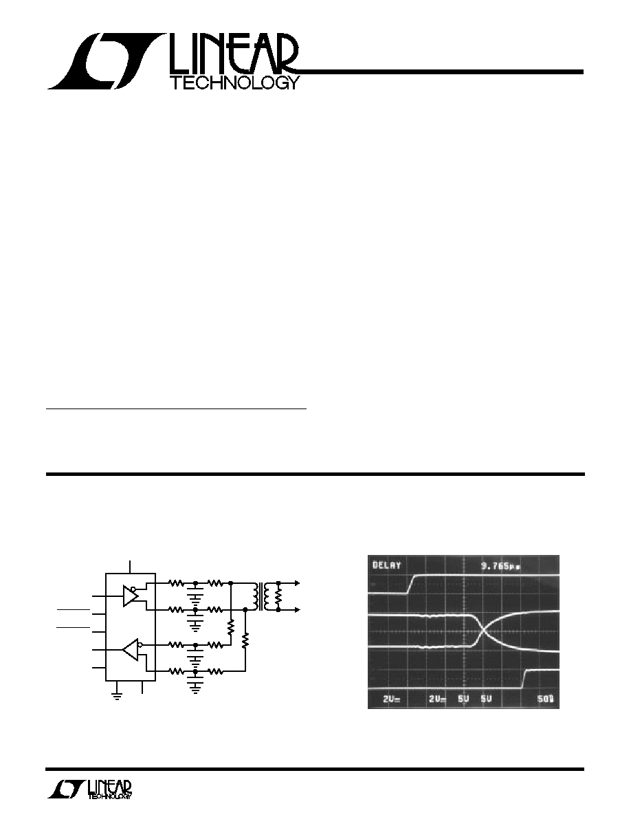
Typical LocalTalk Connection
Output Waveforms
2V/DIV
2V/DIV
5V/DIV
5V/DIV
DATA IN
SIGNALS
ON LINE
DATA OUT
(REMOTE
RECEIVER)
50ns/DIV
U
A
O
PPLICATI
TYPICAL
17 22
100pF
22
16 22
22
11
10
1
3
8
18
5V
5V
9
14
LTC1320
#1
LTC1320 · TA01
100pF
120
LocalTalk
TRANSFORMER
DATA IN
5
4
22
22
22
100pF
22
100pF
1k
1k
DATA OUT
SHUTDOWN
TX ENABLE
RX ENABLE
AppleTalk and LocalTalk are registered trademarks of Apple Computer, Inc.
2
LTC1320
A
U
G
W
A
W
U
W
A
R
BSOLUTE
XI
TI
S
Supply Voltage (V
DD
) ................................................ 7V
Supply Voltage (V
SS
) .............................................. 7V
Input Voltage (Logic Inputs) ......... 0.3V to V
DD
+ 0.3V
Input Voltage (Receiver Inputs) ............................
±
15V
Driver Output Voltage (Forced) .............................
±
15V
Output Short-Circuit Duration ......................... Indefinite
Operating Temperature Range ................... 0
°
C ot 70
°
C
Storage Temperature Range ................ 65
°
c to 150
°
C
Lead Temperature (Soldering, 10 sec)................ 300
°
C
W
U
U
PACKAGE/ORDER I FOR ATIO
ORDER PART
NUMBER
LTC1320CS
SYMBOL
PARAMETER
CONDITIONS
MIN
TYP
MAX
UNITS
V
OD
Differential Driver Output Voltage
No Load
q
8.0
V
R
L
= 100
(Figure 1)
q
2.0
V
Change in Magnitude of Driver
R
L
= 100
(Figure 1)
0.2
V
Differential Output Voltage
V
OC
Driver Common-Mode Output Voltage
R
L
= 100
(Figure 1)
3
V
Output Common-Mode Range
SD = 5V or Power Off
q
±
10
V
Single-Ended Driver Output Voltage
No Load
q
±
4.0
V
R
L
= 400
q
±
3.4
V
Input High Voltage
All Logic Input Pins
q
2.0
V
Input Low Voltage
All Logic Input Pins
q
0.8
V
Input Current
All Logic Input Pins
q
±
1
±
20
µ
A
Three-State Output Current
SD = 5V or Power Off, 10V < V
O
< 10V
q
±
2
±
100
µ
A
Driver Short-Circuit Current
5V < V
O
< 5V
q
35
350
500
mA
Receiver Input Resistance
7V < V
IN
< 7V
q
12
k
V
OH
Receiver Output High Voltage
I
O
= 4mA
q
3.5
V
V
OL
Receiver Output Low Voltage
I
O
= 4mA
q
0.4
V
Receiver Output Short-Circuit Current
0V < V
O
< 5V
q
7
85
mA
Receiver Output Three-State Current
0V < V
O
< 5V
q
±
2
±
100
µ
A
Differential Receiver Threshold Voltage
7V < V
CM
< 7V
q
200
200
mV
Differential Receiver Input Hysteresis
7V < V
CM
< 7V
70
mV
Single-Ended Receiver Input Low Voltage
q
0.8
V
Single-Ended Receiver Input High Voltage
q
2
V
I
DD
Supply Current
No Load, SD = 0V
q
1.2
3.0
mA
No Load, SD = 5V
q
30
350
µ
A
I
SS
Supply Current
No Load, SD = 5V
q
2
350
µ
A
DC ELECTRICAL CHARACTERISTICS
V
S
=
±
5V
±
5%, T
A
= 0
°
C to 70
°
C (Notes 2, 3)
1
2
3
4
5
6
7
8
9
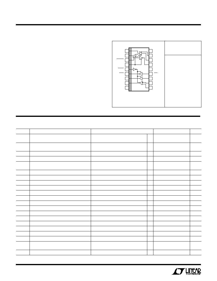
TOP VIEW
18
17
16
15
14
13
12
11
10
TXD
TXI
TXDEN
SD
RXEN
RXO
RXO
RXDO
GND
V
DD
TXD
TXD
+
TXO
V
SS
RXI
RXI
RXD
RXD
+
S PACKAGE
18-LEAD PLASTIC SOL
LTC1320 · PO01
T
JMAX
= 150
°
C,
JA
= 100
°
C/W
Consult factory for Industrial and Military grade parts.
3
LTC1320
SWITCHI G CHARACTERISTICS
U
SYMBOL
PARAMETER
CONDITIONS
MIN
TYP
MAX
UNITS
t
PLH, HL
Differential Driver Propagation Delay
R
L
= 100
, C
L
= 100pF (Figures 2, 8)
q
40
120
ns
t
SKEW
Differential Driver Output to Output
R
L
= 100
, C
L
= 100pF (Figures 2, 8)
q
10
50
ns
t
r, f
Differential Driver Rise/Fall Time
R
L
= 100
, C
L
= 100pF (Figures 2, 8)
q
15
80
ns
t
ENH, L
Driver Enable to Output Active
C
L
= 100pF (Figures 3, 4, 10)
q
50
150
ns
t
H, Ldis
Driver Output Active to Disable
C
L
= 15pF (Figures 3, 4, 10)
q
50
150
ns
t
PLH, HL
Single-Ended Driver Propagation Delay
R
L
= 450
, C
L
= 100pF (Figures 5, 11)
q
40
120
ns
t
r, f
Single-Ended Driver Rise/Fall Time
R
L
= 450
, C
L
= 100pF (Figures 5, 12)
q
15
80
ns
t
PLH, HL
Receiver Propagation Delay
C
L
= 15pF (Figures 13, 14)
q
60
160
ns
t
ENH, L
Receiver Enable to Output Active
C
L
= 100pF (Figures 6, 7, 15)
q
30
100
ns
t
H, Ldis
Receiver Output Active to Disable
C
L
= 15pF (Figures 6, 7, 15)
q
30
100
ns
V
S
=
±
5V
±
5%, T
A
= 0
°
C to 70
°
C (Notes 2, 3)
Note 2: All currents into device pins are positive; all currents out of
device pins are negative. All voltages are referenced to ground unless
otherwise specified.
Note 3: All typicals are given at V
S
=
±
5V, T
A
= 25
°
C.
The
q
denotes specifications which apply over the full operating
temperature range.
Note 1: Absolute Maximum Ratings are those values beyond which the life
of a device may be impaired.
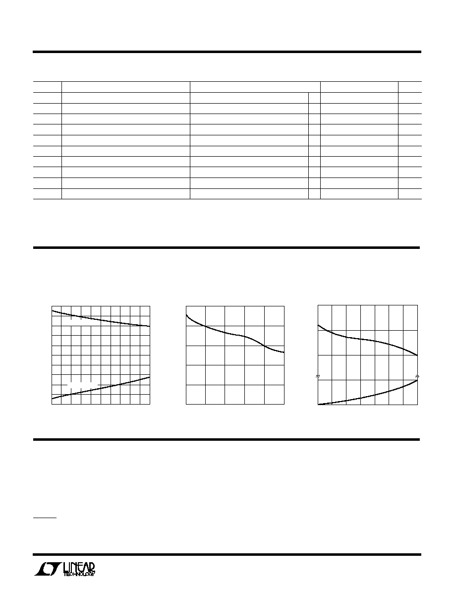
Differential Output Swing vs
Load Current
Output Swing vs Load Current
OUTPUT CURRENT (mA)
0
DIFFERENTIAL OUTPUT SWING (V)
6
8
10
80
LTC1320 · G02
4
2
0
20
40
60
100
Supply Current vs Temperature
C
C
HARA TERISTICS
U
W
A
TYPICAL PERFOR
CE
PI FU CTIO S
U
U
U
TXD (Pin 1): RS422 Differential Driver Input (TTL Compat-
ible).
TXI (Pin 2): RS562 Single-Ended Driver Input (TTL com-
patible.
TXDEN (Pin 3): RS422 Differential Driver Output Enable
(TTL Compatible). A high level on this pin forces the
RS422 driver into three-state; a low level enables the
driver. This input does not affect the RS562 single-ended
driver.
SD (Pin 4): Shutdown Input (TTL Compatible). When this
pin is high, the chip is shut down: all driver outputs three-
state and the supply current drops to 30
µ
A. A low on this
pin allows normal operation.
OUTPUT CURRENT (mA)
0
OUTPUT SWING (V)
1
3
5
80
LTC1320 · G01
1
3
5
20
40
60
100
0
2
4
2
4
OUTPUT HIGH
OUTPUT LOW
TEMPERATURE (°C)
0
0
SUPPLY CURRENT (mA) 0.004
1.0
1.1
1.2
10
20
30
40
LTC1320 · G03
50
60
70
0.002
I
DD
I
SS
4
LTC1320
RXEN (Pin 5): Receiver Enable (TTL Compatible). A high
level on this pin disables the receivers and three-states the
logic outputs; a low level allows normal operation. To
prevent erratic behavior at the receiver outputs during
shutdown, RXEN should be pulled high along with SD.
RXO (Pin 6): Inverting RS562 Single-Ended Receiver
Output.
RXO (Pin 7): Noninverting RS562 Single-Ended Receiver
Output.
RXDO (Pin 8): RS422 Differential Receiver Output.
GND (Pin 9): Ground Pin.
RXD
+
(Pin 10): RS422 Differential Receiver Noninverting
Input. When this pin is
200mV above RXD
, RXDO will
be high; when this pin is
200mV below RXD
, RXDO will
be low.
RXD
(Pin 11): RS422 Differential Receiver Inverting
Input.
PI FU CTIO S
U
U
U
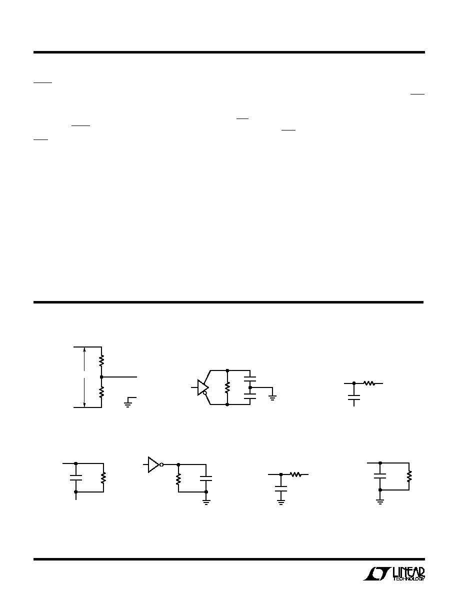
TEST CIRCUITS
RXI (Pin 12): Noninverting RS562 Receiver Input. This
input controls the RXO output; it has no effect on the RXO
output.
RXI (Pin 13): Inverting RS562 Receiver Input. This input
controls the RXO output; it has no effect on the RXO
output.
V
SS
(Pin 14): Negative Supply. 4.75
V
SS
5.25V. The
voltage on this pin must never exceed ground on power up
or power-down.
TXO (Pin 15): RS562 Single-Ended Driver Output.
TXD
+
(Pin 16): RS422 Differential Driver Noninverting
Output.
TXD
(Pin 17): RS422 Differential Driver Inverting Output.
V
DD
(Pin 18): Positive Supply. 4.75V
V
DD
5.25V.
OUTPUT
UNDER TEST
C
L
500
V
DD
V
SS
LTC1320 · F03
Figure 3
R
L
C
L1
C
L2
TXD
LTC1320 · TCF02
TXD
+
TXD
Figure 2
OUTPUT
UNDER TEST
C
L
V
SS
LTC1320 · F04
500
Figure 4
OUTPUT
UNDER TEST
C
L
LTC1320 · F07
500
Figure 7
R
L
C
L
LTC1320 · F05
TXO
TXI
Figure 5
OUTPUT
UNDER TEST
C
L
500
V
DD
LTC1320 · F06
Figure 6
R
L
/2
R
L
/2
V
OC
V
OD
TXD
+
TXD
LTC1320 · F01
+
Figure 1
5
LTC1320
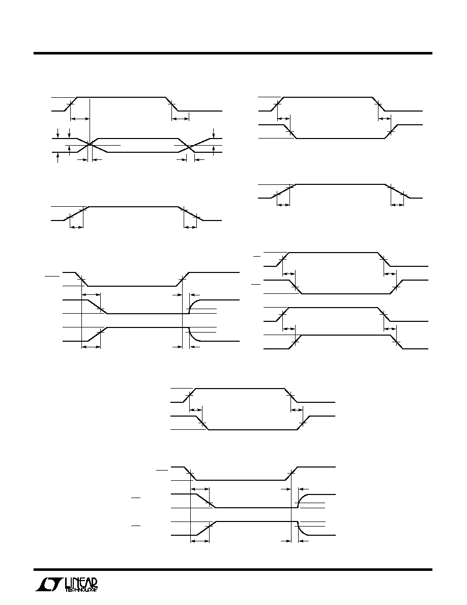
SWITCHI G WAVEFOR S
U
W
t
PHL
1.5V
3V
0V
f = 1MHz: t
r
< 10ns: t
f
< 10ns
1.5V
t
PLH
V
OH
V
OL
1.5V
1.5V
t
PLH
1.5V
3V
0V
RXI
f = 1MHz: t
r
< 10ns: t
f
< 10ns
1.5V
t
PHL
V
OH
V
OL
RXO
1.5V
1.5V
RXI
RXO
LTC1320 · F13
Figure 13
1.5V
t
ENL
3V
0V
1.5V
5V
V
OL
1.5V
V
OH
0V
t
ENH
1.5V
0.5V
0.5V
t
Ldis
f = 1MHz: t
r
10ns: t
f
10ns
OUTPUT NORMALLY LOW
OUTPUT NORMALLY HIGH
RXO, RXO, RXDO
RXO, RXO, RXDO
LTC1320 · F15
t
Hdis
RXEN
Figure 15
1.5V
t
ENL
3V
0V
TXDEN
0V
5V
V
OL
TXD
+
, TXD
0V
V
OH
TXD
+
, TXD
5V
t
ENH
1.5V
0.5V
0.5V
t
Hdis
t
Ldis
f = 1MHz: t
r
10ns: t
f
10ns
OUTPUT NORMALLY LOW
OUTPUT NORMALLY HIGH
LTC1320 · F10
Figure 10
t
PLH
1.5V
3V
0V
TXD
f = 1MHz: t
r
< 10ns: t
f
< 10ns
1.5V
t
PHL
TXD
TXD
+
V
O
t
SKEW
t
SKEW
1/2 V
O
1/2 V
O
LTC1320 · F08
Figure 8
t
PHL
1.5V
3V
0V
TXI
f = 1MHz: t
r
< 10ns: t
f
< 10ns
1.5V
t
PLH
V
OH
V
OL
TXO
0V
0V
LTC1320 · F11
Figure 11
V
O
V
O
90%
10%
t
r
t
f
90%
10%
V
DIFF
= V(TXD
+
) V(TXD
)
LTC1320 · F09
Figure 9
V
OH
V
OL
90%
10%
t
r
t
f
90%
10%
LTC1320 · F12
Figure 12
t
PHL
0V
2.5V
2.5V
(RXD
) (RXD
+
)
f = 1MHz: t
r
< 10ns: t
f
< 10ns
0V
t
PLH
V
OH
V
OL
RXDO
1.5V
1.5V
LTC1320 · F14
Figure 14