Äîêóìåíòàöèÿ è îïèñàíèÿ www.docs.chipfind.ru
1
LTC1326/LTC1326-2.5
Micropower Precision
Triple Supply Monitors
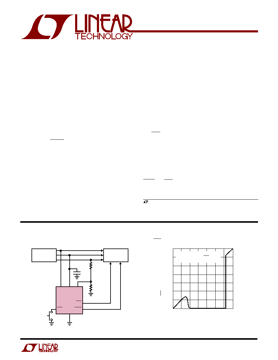
RST Output Voltage vs Supply Voltage (LTC1326-2.5)
s
Simultaneously Monitors Three Supplies
LTC1326: 5V, 3.3V and ADJ
LTC1326-2.5: 2.5V, 3.3V and ADJ
s
Guaranteed Threshold Accuracy:
±
0.75%
s
Low Supply Current: 20
µ
A
s
Internal Reset Time Delay: 200ms
s
Manual Push-Button Reset Input
s
Active Low and Active High Reset Outputs
s
Active Low "Soft" Reset Output
s
Power Supply Glitch Immunity
s
Guaranteed RESET for V
CC3
1V or V
CC5
1V
or V
CC25
1V
s
8-Pin SO and MSOP Packages
FEATURES
The LTC
®
1326/LTC1326-2.5 are triple supply monitors
intended for systems with multiple supply voltages. They
provide micropower operation, small size and high accu-
racy supply monitoring.
Tight 0.75% threshold accuracy and glitch immunity
ensure reliable reset operation without false triggering.
The 20
µ
A typical supply current makes the LTC1326/
LTC1326-2.5 ideal for power-conscious systems.
The RST output is guaranteed to be in the correct state for
V
CC3
,
V
CC5
or V
CC25
down to 1V. The LTC1326/LTC1326-2.5
can be configured to monitor one, two or three inputs,
depending on system requirements.
A manual push-button reset input provides the ability to
generate a very narrow "soft" reset pulse (100
µ
s typ) or a
200ms reset pulse equivalent to a power-on reset. Both
SRST and RST outputs are open-drain and can be OR-tied
with other reset sources.
, LTC and LT are registered trademarks of Linear Technology Corporation.
DESCRIPTIO
U
TYPICAL APPLICATIO
U
s
Desktop Computers
s
Notebook Computers
s
Intelligent Instruments
s
Portable Battery-Powered Equipment
APPLICATIO S
U
V
CC3
(V)
0
2.0
2.5
3.5
1.5
2.5
1326/2.5 TA02
1.5
1.0
0.5
1.0
2.0
3.0
3.5
0.5
0
3.0
RST OUTPUT VOLTAGE (V)
V
CC25
= V
CCA
= V
CC3
4.7k PULL-UP FROM RST TO V
CC3
T
A
= 25
°
C
PUSH-BUTTON
RESET
1326/2.5 TA01
V
CC3
V
CC25
0.1
µ
F
V
CCA
GND
RST
PBR
SRST
LTC1326-2.5
V
CORE
3.3V
2.5V
DC/DC
CONVERTER
SYSTEM
LOGIC
2
LTC1326/LTC1326-2.5
A
U
G
W
A
W
U
W
A
R
BSOLUTE
XI
TI
S
(Notes 1, 2)
Terminal Voltage
V
CC3
, V
CC5
, V
CC25
, V
CCA
......................... 0.5V to 7V
RST, SRST ............................................ 0.5V to 7V
RST ...................................... 0.5V to (V
CC3
+ 0.3V)
PBR .......................................................... 7V to 7V
Operating Temperature Range
LTC1326C/LTC1326C-2.5 ....................... 0
°
C to 70
°
C
LTC1326I/LTC1326I-2.5 ..................... 40
°
C to 85
°
C
Storage Temperature Range ................ 65
°
C to 150
°
C
Lead Temperature (Soldering, 10 sec)................. 300
°
C
W
U
U
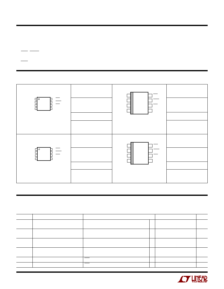
PACKAGE/ORDER I FOR ATIO
ORDER
PART NUMBER
ORDER
PART NUMBER
S8 PART NUMBER
1326
1326I
LTBA
LTC1326CS8
LTC1326IS8
LTC1326CMS8
MS8 PART NUMBER
V
CC3
= 3.3V, V
CC5
= 5V (for LTC1326),V
CC25
= 2.5V (for LTC1326-2.5), V
CCA
= V
CC3
, T
A
= 25
°
C unless otherwise noted.
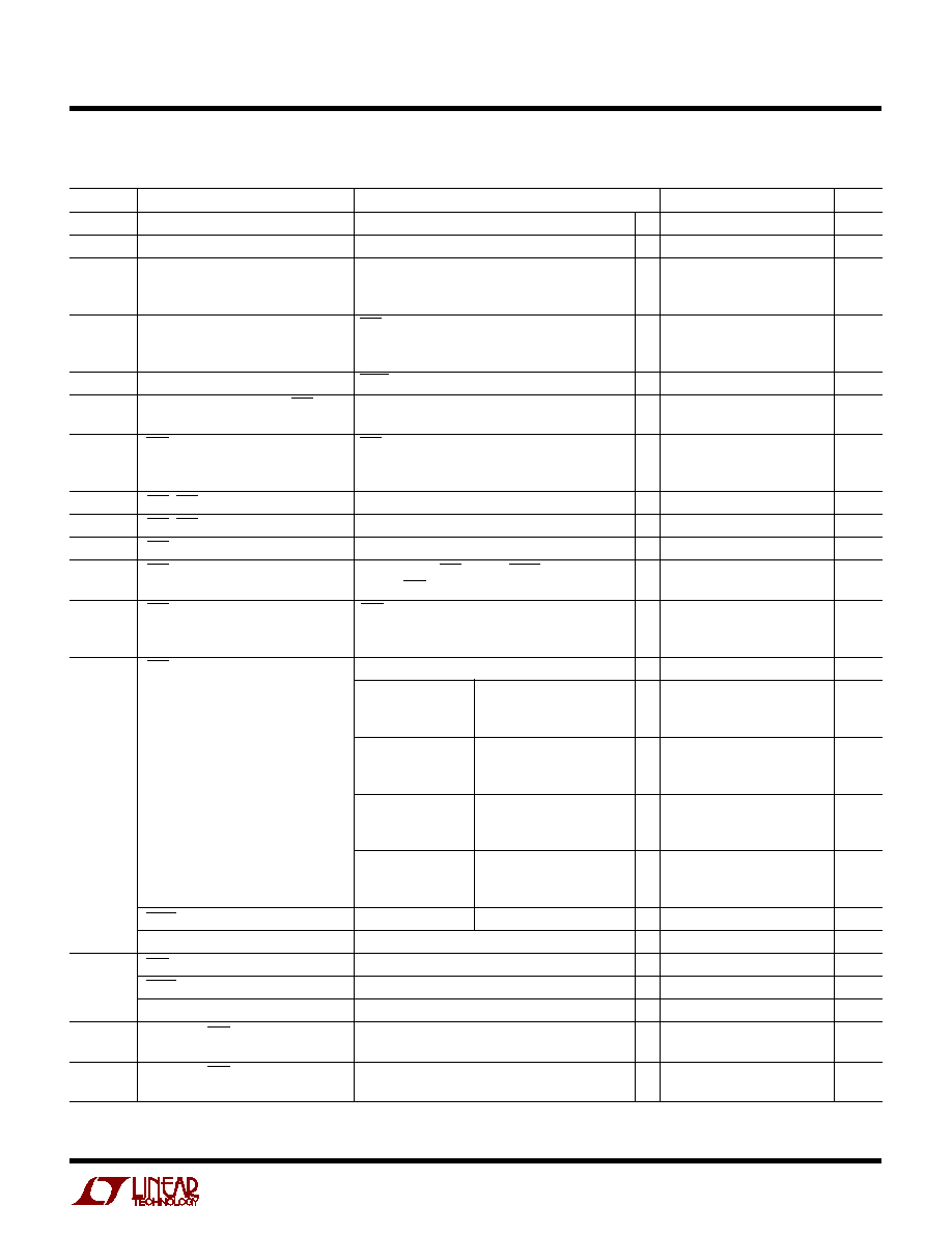
SYMBOL
PARAMETER
CONDITIONS
MIN
TYP
MAX
UNITS
V
RT3
Reset Threshold V
CC3
0
°
C
T
A
70
°
C
q
3.094
3.118
3.143
V
40
°
C
T
A
85
°
C
q
3.052
3.118
3.143
V
V
RT5
Reset Threshold V
CC5
(LTC1326)
0
°
C
T
A
70
°
C
q
4.687
4.725
4.762
V
40
°
C
T
A
85
°
C
q
4.625
4.725
4.762
V
V
RT25
Reset Threshold V
CC25
(LTC1326-2.5)
0
°
C
T
A
70
°
C
q
2.344
2.363
2.381
V
40
°
C
T
A
85
°
C
q
2.312
2.363
2.381
V
V
RTA
Reset Threshold V
CCA
0
°
C
T
A
70
°
C
q
0.992
1.000
1.007
V
40
°
C
T
A
85
°
C
q
0.980
1.000
1.007
V
V
CC
V
CC3
Operating Voltage
RST in Correct Logic State
q
1
7
V
I
VCC3
V
CC3
Supply Current
PBR = V
CC3
q
20
40
µ
A
ELECTRICAL CHARACTERISTICS
ORDER
PART NUMBER
ORDER
PART NUMBER
S8 PART MARKING
MS8 PART MARKING
LTC1326CS8-2.5
LTC1326IS8-2.5
LTC1326CMS8-2.5
132625
326I25
LTEK
Consult factory for Military grade parts.
1
2
3
4
8
7
6
5
TOP VIEW
S8 PACKAGE
8-LEAD PLASTIC SO
V
CC3
V
CC5
V
CCA
GND
PBR
SRST
RST
RST
T
JMAX
= 125
°
C,
JA
= 150
°
C/W
1
2
3
4
V
CC3
V
CC5
V
CCA
GND
8
7
6
5
PBR
SRST
RST
RST
TOP VIEW
MS8 PACKAGE
8-LEAD PLASTIC MSOP
T
JMAX
= 125
°
C,
JA
= 250
°
C/W
1
2
3
4
8
7
6
5
TOP VIEW
S8 PACKAGE
8-LEAD PLASTIC SO
V
CC3
V
CC25
V
CCA
GND
PBR
SRST
RST
RST
T
JMAX
= 125
°
C,
JA
= 150
°
C/W
1
2
3
4
V
CC3
V
CC25
V
CCA
GND
8
7
6
5
PBR
SRST
RST
RST
TOP VIEW
MS8 PACKAGE
8-LEAD PLASTIC MSOP
T
JMAX
= 125
°
C,
JA
= 250
°
C/W
3
LTC1326/LTC1326-2.5
I
VCC5
V
CC5
Input Current (LTC1326)
V
CC5
= 5V
q
4
7
µ
A
I
VCC25
V
CC25
Input Current (LTC1326-2.5)
V
CC25
= 2.5V
q
2.8
7
µ
A
I
VCCA
V
CCA
Input Current
V
CCA
= 1V
0
°
C
T
A
70
°
C
q
5
0
5
nA
40
°
C
T
A
85
°
C
q
15
0
15
nA
t
RST
Reset Pulse Width
RST Low with 10k
Pull-Up to V
CC3
0
°
C
T
A
70
°
C
q
140
200
280
ms
40
°
C
T
A
85
°
C
q
140
200
300
ms
t
SRST
Soft Reset Pulse Width
SRST Low with 10k
Pull-Up to V
CC3
q
50
100
200
µ
s
t
UV
V
CC
Undervoltage Detect to RST
V
CC25
, V
CC3
or V
CCA
Less Than Reset
13
µ
s
Threshold V
RT
by More Than 1%
I
PBR
PBR Pull-Up Current
PBR = 0V
0
°
C
T
A
70
°
C
q
3
7
10
µ
A
40
°
C
T
A
85
°
C
q
3
7
15
µ
A
V
IL
PBR, RST Input Low Voltage
q
0.8
V
V
IH
PBR, RST Input High Voltage
q
2
V
t
PW
PBR Min Pulse Width
q
40
ns
t
DB
PBR Debounce
Deassertion of PBR Input to SRST
q
20
35
ms
Output (PBR Pulse Width = 1
µ
s)
t
PB
PBR Assertion Time for Transition
PBR Held Less Than V
IL
from Soft to Hard Reset Mode
0
°
C
T
A
70
°
C
q
1.4
2.0
2.8
s
40
°
C
T
A
85
°
C
q
1.4
2.0
3.0
s
V
OL
RST Output Voltage Low
I
SINK
= 5mA
q
0.15
0.4
V
I
SINK
= 100
µ
A,
V
CC3
= 1V, V
CC5
= 0V
q
0.05
0.4
V
0
°
C
T
A
70
°
C
V
CC3
= 0V, V
CC5
= 1V
q
0.05
0.4
V
V
CC3
= 1V, V
CC5
= 1V
q
0.05
0.4
V
I
SINK
= 100
µ
A,
V
CC3
= 1.1V, V
CC5
= 0V
q
0.05
0.4
V
40
°
C
T
A
85
°
C
V
CC3
= 0V, V
CC5
= 1.1V
q
0.05
0.4
V
V
CC3
= 1.1V, V
CC5
= 1.1V
q
0.05
0.4
V
I
SINK
= 100
µ
A,
V
CC3
= 1V, V
CC25
= 0V
q
0.05
0.4
V
0
°
C
T
A
70
°
C
V
CC3
= 0V, V
CC25
= 1V
q
0.05
0.4
V
V
CC3
= 1V, V
CC25
= 1V
q
0.05
0.4
V
I
SINK
= 100
µ
A,
V
CC3
= 1.1V, V
CC25
= 0V
q
0.05
0.4
V
40
°
C
T
A
85
°
C
V
CC3
= 0V, V
CC25
= 1.1V
q
0.05
0.4
V
V
CC3
= 1.1V, V
CC25
= 1.1V
q
0.05
0.4
V
SRST Output Voltage Low
I
SINK
= 2.5mA
q
0.15
0.4
V
RST Output Voltage Low
I
SINK
= 2.5mA
q
0.15
0.4
V
V
OH
RST Output Voltage High (Note 3)
I
SOURCE
= 1
µ
A
q
V
CC3
1
V
SRST Output Voltage High (Note 3)
I
SOURCE
= 1
µ
A
q
V
CC3
1
V
RST Output Voltage High
I
SOURCE
= 600
µ
A
q
V
CC3
1
V
t
PHL
Prop Delay RST to RST
C
RST
= 20pF
25
ns
High Input to Low Output
t
PLH
Prop Delay RST to RST
C
RST
= 20pF
45
ns
Low Input to High Output
ELECTRICAL CHARACTERISTICS
V
CC3
= 3.3V, V
CC5
= 5V (for LTC1326),V
CC25
= 2.5V (for LTC1326-2.5), V
CCA
= V
CC3
, T
A
= 25
°
C unless otherwise noted.
SYMBOL
PARAMETER
CONDITIONS
MIN
TYP
MAX
UNITS
4
LTC1326/LTC1326-2.5
ELECTRICAL CHARACTERISTICS
LTC1326 Only V
CC3
= 3.3V, V
CC5
= 5V, V
CCA
= V
CC3
, T
A
= 25
°
C unless otherwise noted.
SYMBOL
PARAMETER
CONDITIONS
MIN
TYP
MAX
UNITS
V
OVR
V
CC5
Reset Override Voltage
Override V
CC5
Ability to Assert RST (Note 4)
V
CC3
±
0.025
V
Note 3: The output pins SRST and RST have weak internal pull-ups to
V
CC3
of 6
µ
A typ. However, external pull-up resistors may be used when
faster rise times are required.
Note 4: The V
CC5
reset override voltage is valid for an operating range less
than approximately 4.15V. Above this point the override is turned off and
the V
CC5
pin functions normally.
The
q
denotes specifications which apply over the full operating
temperature range.
Note 1: Absolute Maximum Ratings are those values beyond which the life
of the device may be impaired.
Note 2: All voltage values are with respect to GND.
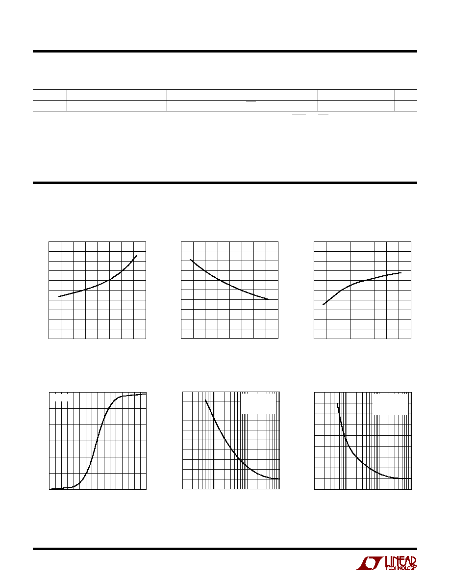
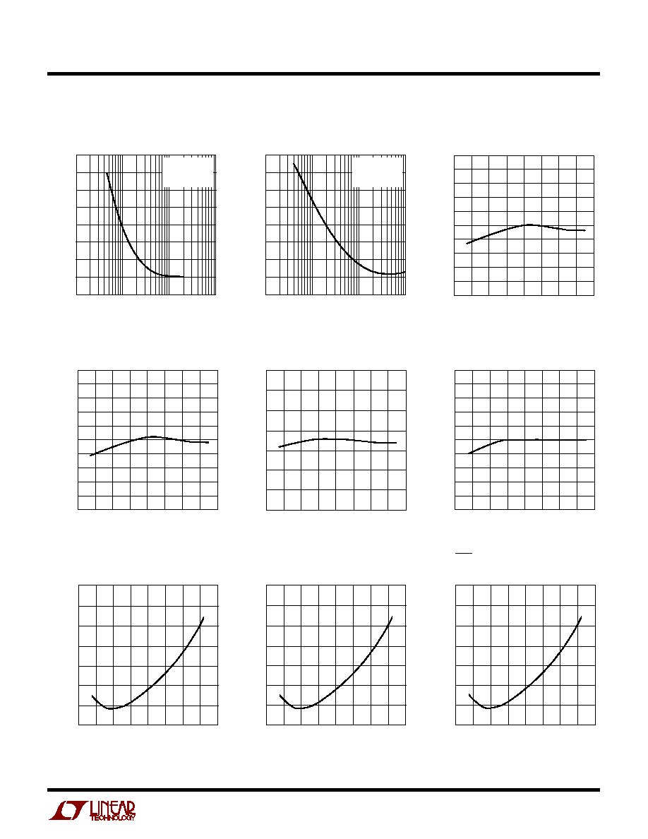
TYPICAL PERFOR A CE CHARACTERISTICS
U
W
TEMPERATURE (
°
C)
15
I
VCC3
(
µ
A)
16
18
19
20
25
22
1326
/2.5
G01
17
23
24
21
60
20
20
40
40
0
60
80
100
I
VCC3
vs Temperature
TEMPERATURE (
°
C)
2.50
I
VCC25
(
µ
A)
2.55
2.65
2.70
2.75
3.00
2.85
1326
/2.5
G03
2.60
2.90
2.95
2.80
60
20
20
40
40
0
60
80
100
I
VCC25
vs Temperature
(LTC1326-2.5)
TEMPERATURE (
°
C)
I
VCC5
(
µ
A)
5.0
4.8
4.6
4.4
4.2
4.0
3.8
3.6
3.4
3.2
3.0
1326
/2.5
G02
60
20
20
40
40
0
60
80
100
I
VCC5
vs Temperature
(LTC1326)
V
CC5
Transient Immunity
(LTC1326)
V
CC5
RESET COMPARATOR OVERDRIVE (V)
0.001
20
TRANSIENT DURATION (
µ
s)
25
30
35
40
0.01
0.1
1
1326/2.5 G05
15
10
5
0
45
50
RESET OCCURS
ABOVE CURVE
T
A
= 25
°
C
V
CCA
Input Current vs Input Voltage
INPUT VOLTAGE (V)
0.8
3
INPUT CURRENT (nA)
2
1
0
1
0.9
1.0
1.1
1.2
1326
/2.5
G04
2
3
0.85
0.95
1.05
1.15
T
A
= 25
°
C
V
CC25
Transient Immunity
(LTC1326-2.5)
V
CC25
RESET COMPARATOR OVERDRIVE (V)
0.001
TRANSIENT DURATION (
µ
s)
0.01
0.1
1
1326/2.5 G06
45
40
35
30
25
20
15
10
5
0
RESET OCCURS
ABOVE CURVE
T
A
= 25
°
C
5
LTC1326/LTC1326-2.5
TYPICAL PERFOR A CE CHARACTERISTICS
U
W
TEMPERATURE (
°
C)
60
V
CC25
THRESHOLD VOLTAGE, V
RT25
(V)
2.375
2.370
2.365
2.360
2.355
2.350
20
20
40
1326
/2.5
G10
40
0
60
80
100
V
CC25
Threshold Voltage
vs Temperature (LTC1326-2.5)
TEMPERATURE (
°
C)
60
V
CCA
THRESHOLD VOLTAGE, V
RTA
(V)
1.005
1.004
1.003
1.002
1.001
1.000
0.999
0.998
0.997
0.996
0.995
20
20
40
1326
/2.5
G12
40
0
60
80
100
V
CCA
Threshold Voltage
vs Temperature
V
CC3
Threshold Voltage
vs Temperature
TEMPERATURE (
°
C)
60
V
CC3
THRESHOLD VOLTAGE, V
RT3
(V)
60
1326
/2.5
G11
20
20
40
80
0
40
100
3.135
3.130
3.125
3.120
3.115
3.110
3.105
3.100
Reset Pulse Width
vs Temperature
PBR Assertion Time to Reset
vs Temperature
"Soft" Reset Pulse Width
vs Temperature
TEMPERATURE (
°
C)
210
215
220
1326
/2.5
G13
205
200
195
190
RESET PULSE WIDTH, t
RST
(ms)
225
60
20
20
40
40
0
60
80
100
TEMPERATURE (
°
C)
105.0
107.5
110.0
1326
/2.5
G14
102.5
100.0
97.5
95.0
SOFT RESET PULSE WIDTH, t
SRST
(
µ
s)
112.5
60
20
20
40
40
0
60
80
100
TEMPERATURE (
°
C)
2.10
2.15
2.20
1326
/2.5
G15
2.05
2.00
1.95
1.90
PBR ASSERTION TIME TO RESET, t
PB
(SEC)
2.25
60
20
20
40
40
0
60
80
100
V
CCA
Transient Immunity
V
CCA
RESET COMPARATOR OVERDRIVE (V)
0.001
20
TRANSIENT DURATION (
µ
s)
30
40
0.01
0.1
1
1326/2.5 G07
10
0
25
35
15
5
RESET OCCURS
ABOVE CURVE
T
A
= 25
°
C
V
CC3
RESET COMPARATOR OVERDRIVE (V)
0.001
20
TRANSIENT DURATION (
µ
s)
30
40
0.01
0.1
1
1326/2.5 G08
10
0
25
35
15
5
RESET OCCURS
ABOVE CURVE
T
A
= 25
°
C
V
CC3
Transient Immunity
TEMPERATURE (
°
C)
60
V
CC5
THRESHOLD VOLTAGE, V
RT5
(V)
4.750
4.745
4.740
4.735
4.730
4.725
4.720
4.715
4.710
4.705
4.700
20
20
40
1326
/2.5
G09
40
0
60
80
100
V
CC5
Threshold Voltage
vs Temperature (LTC1326)