 | –≠–ª–µ–∫—Ç—Ä–æ–Ω–Ω—ã–π –∫–æ–º–ø–æ–Ω–µ–Ω—Ç: LTC1338C | –°–∫–∞—á–∞—Ç—å:  PDF PDF  ZIP ZIP |
1
LTC1338
5V Low Power RS232
5-Driver/3-Receiver Transceiver
S
FEATURE
D
U
ESCRIPTIO
s
Low Supply Current: 500
µ
A
s
0.2
µ
A Supply Current in SHUTDOWN
s
50
µ
A Supply Current in RECEIVER ALIVE Mode
s
ESD Protection Over
±
10kV
s
Operates from a Single 5V Supply
s
Uses Small Capacitors: 0.1
µ
F
s
Operates to 120k Baud
s
Three-State Outputs Are High Impedance When Off
s
Output Overvoltage Does Not Force Current
Back into Supplies
s
RS232 I/O Lines Can Be Forced to
±
25V
Without Damage
s
Flowthrough Architecture
The LTC1338 is a 5-driver/ 3-receiver RS232 trans-
ceiver with very low supply current. In the no load
condition, the supply current is only 500
µ
A. The charge
pump only requires four 0.1
µ
F capacitors.
In SHUTDOWN mode, the supply current is further
reduced to 0.2
µ
A. In RECEIVER ALIVE mode, all three
receivers are kept alive and the supply current is 50
µ
A.
All RS232 outputs assume a high impedance state in
SHUTDOWN and with the power off.
The LTC1338 is fully compliant with all data rate and
overvoltage RS232 specifications. The transceiver can
operate up to 120k baud with a 2500pF, 3k
load. Both
driver outputs and receiver inputs can be forced to
±
25V without damage, and can survive multiple
±
10kV
ESD strikes.
U
S
A
O
PPLICATI
s
Battery-Powered Modems
s
Battery-Powered DCE
s
Notebook Computers
s
Palmtop Computers
U
A
O
PPLICATI
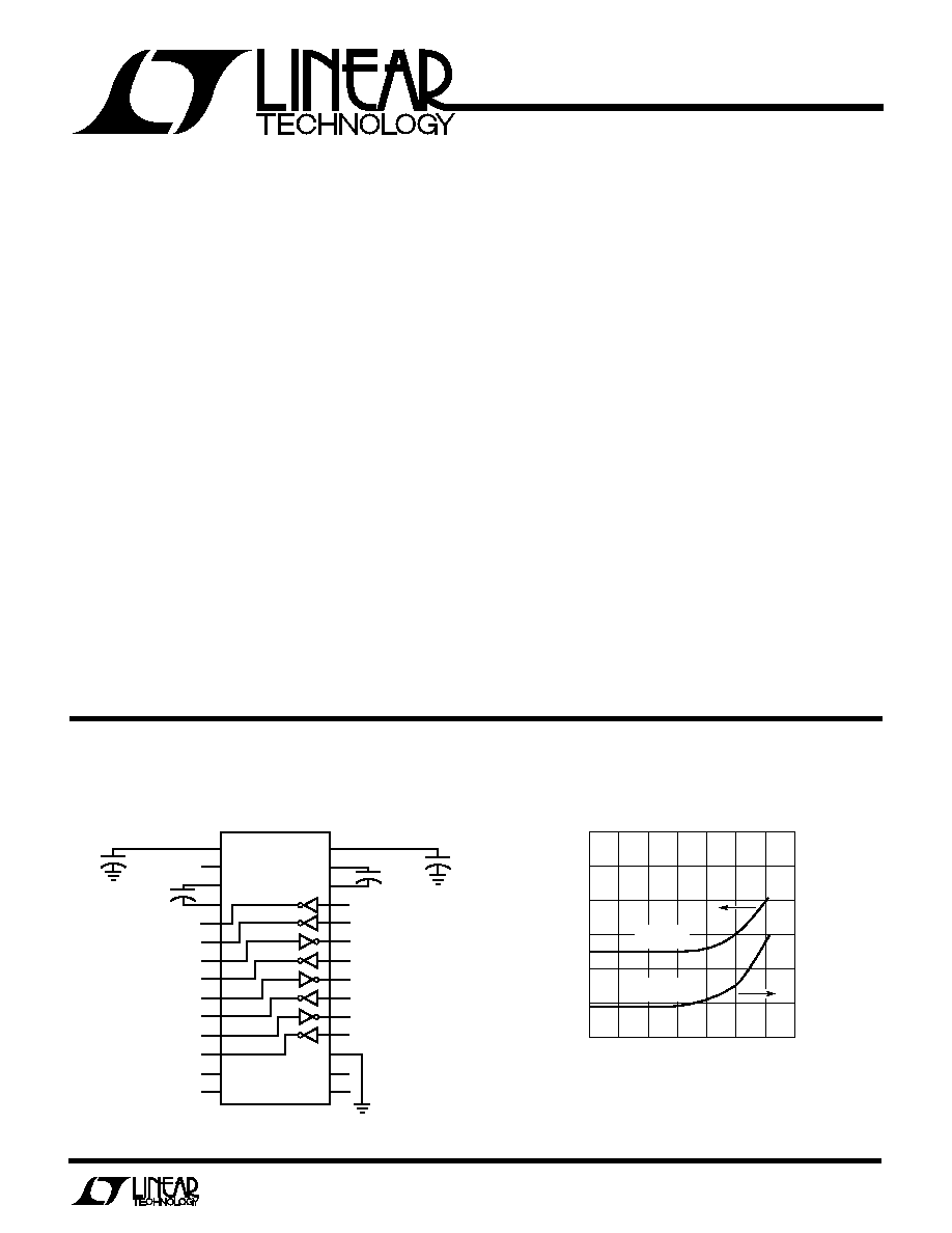
TYPICAL
5-Drivers/3-Receivers with SHUTDOWN
LTC1338 ∑ TA01
V
CC
C1
0.1
µ
F
LTC1338
1
2
3
4
5
6
7
8
9
10
11
12
13
14
DRIVER 1 OUT
DRIVER 2 OUT
RX1 IN
DRIVER 3 OUT
RX2 IN
DRIVER 4 OUT
RX3 IN
DRIVER 5 OUT
RX ENABLE
NC
28
27
26
25
24
23
22
21
20
19
18
17
16
15
C3
0.1
µ
F
DRIVER 1 IN
DRIVER 2 IN
RX1 OUT
DRIVER 3 IN
RX2 OUT
DRIVER 4 IN
RX3 OUT
DRIVER 5 IN
GND
DRIVER ENABLE
NC
V
≠
V
+
C2
0.1
µ
F
C4
0.1
µ
F
TEMPERATURE (∞C)
QUIESCENT CURRENT (
µ
A)
1200
1000
800
600
400
200
0
20
40
60
LTC1338 ∑ TA02
80
0
≠20
1.2
1.0
0.8
0.6
0.4
0.2
0
SHUTDOWN CURRENT (
µ
A)
QUIESCENT
CURRENT
SHUTDOWN
CURRENT
≠40
TEST CONDITION:
V
CC
= 5V, ALL DRIVER INPUTS TIED TO V
CC
.
100
Supply Current
2
LTC1338
A
U
G
W
A
W
U
W
A
R
BSOLUTE
XI
TI
S
W
U
U
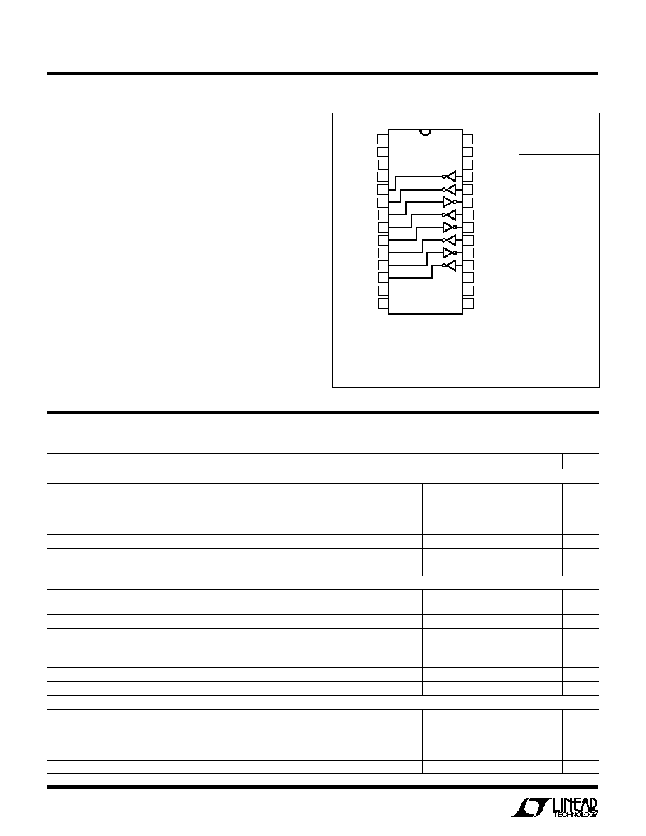
PACKAGE/ORDER I FOR ATIO
ORDER PART
NUMBER
1
2
3
4
5
6
7
8
9
10
11
12
13
14
V
+
V
CC
C1
+
C1
≠
DR1 OUT
DR2 OUT
RX1 IN
DR3 OUT
RX2 IN
DR4 OUT
RX3 IN
DR5 OUT
RX ENABLE
NC
28
27
26
25
24
23
22
21
20
19
18
17
16
15
V
≠
C2
+
C2
≠
DR1 IN
DR2 IN
RX1 OUT
DR3 IN
RX2 OUT
DR4 IN
RX3 OUT
DR5 IN
GND
DR ENABLE
NC
N PACKAGE
28-LEAD PLASTIC DIP
TOP VIEW
S PACKAGE
28-LEAD PLASTIC SOL
G PACKAGE
28-LEAD SSOP
T
JMAX
= 125
∞
C,
JA
= 96
∞
C/W (G)
T
JMAX
= 125
∞
C,
JA
= 56
∞
C/W (N)
T
JMAX
= 125
∞
C,
JA
= 85
∞
C/W (S)
PARAMETER
CONDITIONS
MIN
TYP
MAX
UNITS
Any Driver
Output Voltage Swing
3k to GND
Positive
q
5.0
7.0
V
Negative
q
≠ 5.0
≠ 6.5
V
Logic Input Voltage Level
Input Low Level (V
OUT
= High)
q
1.4
0.8
V
Input High Level (V
OUT
= Low)
q
2.0
1.4
V
Logic Input Current
0
V
IN
V
CC
q
±
5
µ
A
Output Short-Circuit Current
V
OUT
= 0V
±
12
mA
Output Leakage Current
SHUTDOWN, V
OUT
=
±
20V (Note 3)
q
±
10
±
500
µ
A
Any Receiver
Input Voltage Thresholds
Input Low Threshold
q
0.8
1.3
V
Input High Threshold
q
1.7
2.4
V
Hysteresis
q
0.1
0.4
1
V
Input Resistance
≠ 10V
V
IN
10V
3
5
7
k
Output Voltage
Output Low, I
OUT
= ≠ 1.6mA (V
CC
= 5V)
q
0.2
0.4
V
Output High, I
OUT
= 160
µ
A (V
CC
= 5V)
q
3.5
4.8
V
Output Short-Circuit Current
Sinking Current, V
OUT
= V
CC
≠ 15
≠ 40
mA
Output Leakage Current
SHUTDOWN, 0
V
OUT
V
CC
(Note 3)
q
1
10
µ
A
Power Supply Generator
V
+
Output Voltage
I
OUT
= 0mA
8.0
V
I
OUT
= 12mA
7.5
V
V
≠
Output Voltage
I
OUT
= 0mA
≠ 8.0
V
I
OUT
= ≠ 12mA
≠ 7.0
V
Supply Rise Time
SHUTDOWN to Turn-On
0.2
ms
LTC1338CG
LTC1338CN
LTC1338CS
LTC1338IG
LTC1338IN
LTC1338IS
Supply Voltage (V
CC
) ................................................ 6V
Input Voltage
Driver ....................................... ≠ 0.3V to V
CC
+ 0.3V
Receiver ............................................... ≠ 25V to 25V
Driver/Receiver Enable Pin ........ ≠ 0.3V to V
CC
+ 0.3V
Output Voltage
Driver .................................................... ≠ 25V to 25V
Receiver .................................... ≠ 0.3V to V
CC
+ 0.3V
Short Circuit Duration
V
+
................................................................... 30 sec
V
≠
................................................................... 30 sec
Driver Output .............................................. Indefinite
Receiver Output .......................................... Indefinite
Operating Temperature Range
Commercial (LTC1338C) ........................ 0
∞
C to 70
∞
C
Industrial (LTC1338I) ........................ ≠ 40
∞
C to 85
∞
C
Storage Temperature Range ................ ≠ 65
∞
C to 150
∞
C
Lead Temperature (Soldering, 10 sec) ................. 300
∞
C
(Note 1)
V
CC
= 5V, C1 = C2 = C3 = C4 = 0.1
µ
F, unless otherwise noted.
ELECTRICAL C
C
HARA TERISTICS
C
D
3
LTC1338
V
CC
= 5V, C1 = C2 = C3 = C4 = 0.1
µ
F, unless otherwise noted.
ELECTRICAL C
C
HARA TERISTICS
C
D
C
C
HARA TERISTICS
AC
Note 3: Supply current and leakage current measurements in SHUTDOWN
are performed with V
DRIVER ENABLE
and V
RECEIVER ENABLE
= 0V.
Note 4: Supply current measurement in RECEIVER ALIVE mode is
performed with V
DRIVER ENABLE
= 0V and V
RECEIVER ENABLE
= V
CC
.
The
q
denotes specifications which apply over the operating temperature
range of 0
∞
C to 70
∞
C or ≠ 40
∞
C to 85
∞
C.
Note 1: Absolute maximum ratings are those values beyond which the life
of the device may be impaired.
Note 2: Supply current is measured with driver and receiver outputs
unloaded. The V
DRIVER ENABLE
and V
RECEIVER ENABLE
= V
CC
.
PARAMETER
CONDITIONS
MIN
TYP
MAX
UNITS
Slew Rate
R
L
= 3k, C
L
= 51pF
8
30
V/
µ
s
R
L
= 3k, C
L
= 2500pF
3
5
V/
µ
s
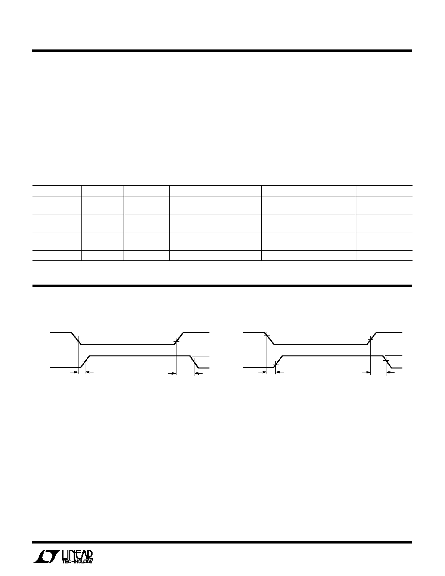
Driver Propagation Delay
t
HLD
(Figure 1)
q
2
3.5
µ
s
(TTL to RS232)
t
LHD
(Figure 1)
q
2
3.5
µ
s
Receiver Propagation Delay
t
HLR
(Figure 2)
q
0.3
0.8
µ
s
(RS232 to TTL)
t
LHR
(Figure 2)
q
0.2
0.8
µ
s
V
CC
= 5V, C1 = C2 = C3 = C4 = 0.1
µ
F, unless otherwise noted.
TYPICAL PERFOR A CE CHARACTERISTICS
W U
DATA RATE (k BAUD)
0
SUPPLY CURRENT (mA)
40
50
60
60
100
LTC1338 ∑ TPC03
30
20
20
40
80
120
140
10
0
V
CC
= 5V
R
L
= 3k
C
L
= 2500pF
5 DRIVERS ACTIVE
TEMPERATURE (∞C)
≠40
THRESHOLD VOLTAGE (V)
1.8
2.0
2.2
20
60
LTC1338 ∑ TPC02
1.6
1.4
≠20
0
40
80
100
1.2
1.0
V
TH
V
TL
TEMPERATURE (∞C)
≠40
≠8
DRIVER OUTPUT VOLTAGE (V)
≠6
≠2
0
2
40
10
LTC1338 ∑ TPC01
≠4
0
80
4
6
8
≠20
60
20
100
R
L
= 3k
OUTPUT HIGH
V
CC
= 5V
V
CC
= 4.5V
OUTPUT LOW
V
CC
= 4.5V
V
CC
= 5V
Driver Output Voltage
Receiver Input Thresholds
Supply Current vs Data Rate
PARAMETER
CONDITIONS
MIN
TYP
MAX
UNITS
Power Supply
V
CC
Supply Current
No Load (All Driver V
IN
= V
CC
)(Note 2) 0
∞
C
T
A
70
∞
C
0.5
1.0
mA
No Load (All Driver V
IN
= 0V)(Note 2) 0
∞
C
T
A
70
∞
C
1.0
1.5
mA
No Load (All Driver V
IN
= V
CC
)(Note 2) ≠ 40
∞
C
T
A
85
∞
C
0.5
1.5
mA
No Load (All Driver V
IN
= 0V)(Note 2) ≠ 40
∞
C
T
A
85
∞
C
1.0
2.0
mA
RECEIVER ALIVE Mode (Note 4)
q
50
80
µ
A
Supply Leakage Current (V
CC
)
SHUTDOWN (Note 3)
q
0.2
10
µ
A
Driver/Receiver Enable Threshold Low
q
1.4
0.8
V
Driver/Receiver Enable Threshold High
q
2.0
1.4
V
4
LTC1338
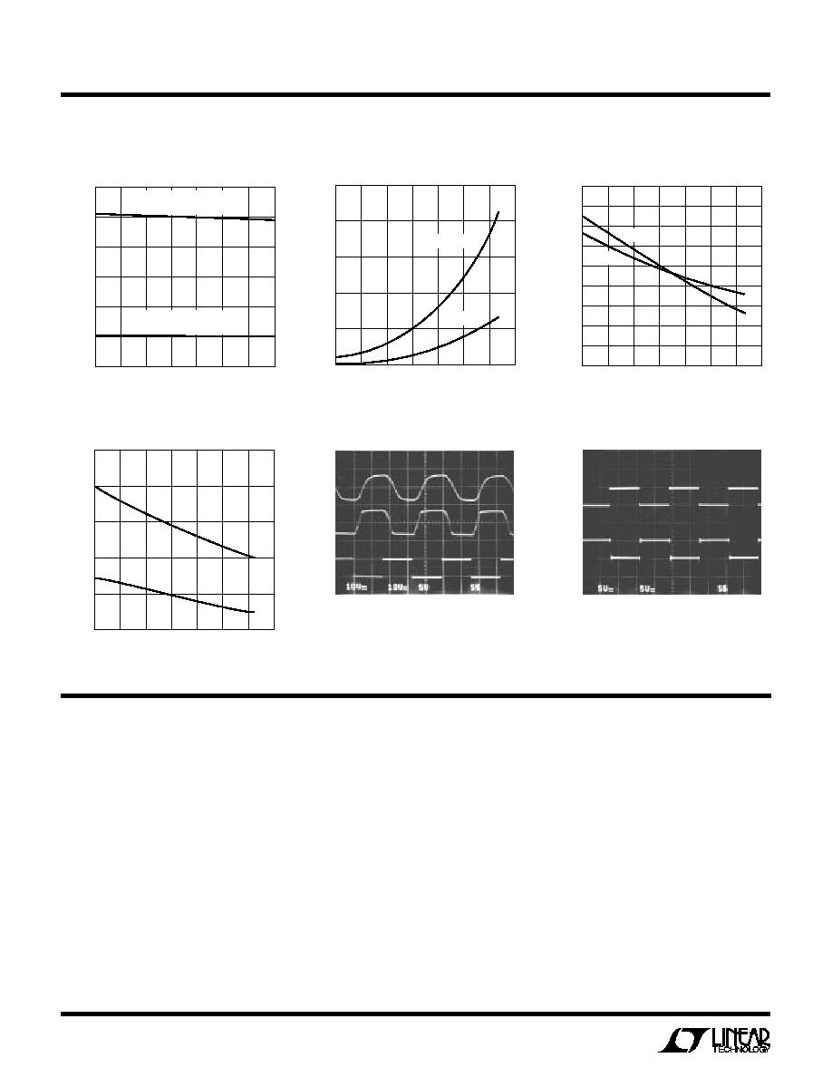
TYPICAL PERFOR A CE CHARACTERISTICS
W U
V
CC
Supply Current
Driver Leakage in Shutdown
Driver Short-Circuit Current
TEMPERATURE (∞C)
≠40
SUPPLY CURRENT (mA)
20
25
30
20
60
LTC1338 ∑ TPC04
15
10
≠20
0
40
80
100
5
0
5 DRIVERS LOADED
R
L
= 3k
1 DRIVER LOADED
R
L
= 3k
TEMPERATURE (∞C)
≠40
0
SHORT-CIRCUIT CURRENT (mA)
4
8
10
12
40
20
LTC1338 ∑ TPC06
6
0
80
14
16
18
≠20
60
20
100
I
SC
+
I
SC
≠
TEMPERATURE (∞C)
≠40
0
LEAKAGE CURRENT (
µ
A)
20
50
0
40
60
LTC1338 ∑ TPC05
10
40
30
≠20
20
80
100
V
OUT
= ≠20V
V
OUT
= 20V
Receiver Short-Circuit Current
Driver Output Waveforms
Receiver Output Waveforms
TEMPERATURE (∞C)
≠40
10
SHORT-CIRCUIT CURRENT (mA)
30
60
0
40
60
LTC1338 ∑ TPC07
20
50
40
≠20
20
80
100
I
SC
≠
I
SC
+
DRIVER
OUTPUT
R
L
= 3k
C
L
= 2500pF
DRIVER
OUTPUT
R
L
= 3k
INPUT
LTC1338 ∑ TPC08
LTC1338 ∑ TPC09
RECEIVER
OUTPUT
C
L
= 50pF
INPUT
PI FU CTIO S
U
U
U
V
CC
: 5V Input Supply Pin. Supply current less than 0.2
µ
A
in the SHUTDOWN mode. This pin should be decoupled
with a 0.1
µ
F ceramic capacitor.
GND: Ground Pin.
RECEIVER ENABLE: TTL/CMOS Compatible Enable Pin.
Refer to Table 1 for its functional description. This pin can
not float.
DRIVER ENABLE: TTL/CMOS Compatible Enable Pin. Re-
fer to Table 1 for its functional description. This pin can not
float.
V
+
: Positive Supply Output (RS232 Drivers). V
+
2V
CC
≠
1V. This pin requires an external capacitor C = 0.1
µ
F for
charge storage. The capacitor may be tied to ground or 5V.
With multiple devices, the V
+
and V
≠
pins may be paral-
leled into common capacitors. For large numbers of
devices, increasing the size of the shared common storage
capacitors is recommended to reduce ripple.
V
≠
: Negative Supply Output (RS232 Drivers). V
≠
2V
CC
≠ 1.5V. This pin requires an external capacitor C = 0.1
µ
F for
charge storage.
C1
+
, C1
≠
, C2
+
, C2
≠
: Commutating Capacitor Inputs. These
pins require two external capacitors C = 0.1
µ
F: one from
C1
+
to C1
≠
, and another from C2
+
to C2
≠
. To maintain
charge pump efficiency, the capacitor's effective series
resistance should be less than 20
.
5
LTC1338
PI FU CTIO S
U
U
U
DRIVER IN: RS232 Driver Input Pins. Inputs are TTL/
CMOS compatible. Inputs should not be allowed to float.
Tie unused inputs to V
CC
.
DRIVER OUT: Driver Outputs at RS232 Voltage Levels.
Outputs are in a high impedance state when in SHUT-
DOWN, RECEIVER ALIVE mode or V
CC
= 0V. The driver
outputs are protected against ESD to
±
10kV for human
body model discharges.
RX IN: Receiver Inputs. These pins can be forced to
±
25V
without damage. The receiver inputs are protected against
ESD to
±
10kV for human body model discharges. Each
receiver provides 0.4V of hysteresis for noise immunity.
RX OUT: Receiver Outputs with TTL/CMOS Voltage Lev-
els. Outputs are in a high impedance state when in SHUT-
DOWN or RECEIVER DISABLE mode to allow data line
sharing.
Table 1. Functional Description
MODE
RX ENABLE
DR ENABLE
DRIVERS
RECEIVERS
I
CC
(
µ
A)(TYP)
SHUTDOWN
0
0
All driver outputs are
All receiver outputs are
0.2
high impedance.
high impedance.
Receiver Disable
0
1
All drivers alive.
All receiver outputs are
500
high impedance.
RECEIVER ALIVE
1
0
All driver outputs are
All receivers alive.
50
high impedance.
Normal
1
1
All drivers alive.
All receivers alive.
500
TI
W
E WAVEFOR
S
U
G
WITCHI
W
S
Figure 1. Driver Propagation Delay Timing
Figure 2. Receiver Propagation Delay Timing
1.4V
0V
V
CC
0V
V
+
V
≠
0V
DRIVER
INPUT
DRIVER
OUTPUT
1.4V
t
HLD
t
LHD
LTC1338 ∑ F01
0.8V
V
CC
0V
2.4V
RX
INPUT
RX
OUTPUT
1.3V
t
HLR
1.7V
t
LHR
LTC1338 ∑ F02
V
CC
0V
6
LTC1338
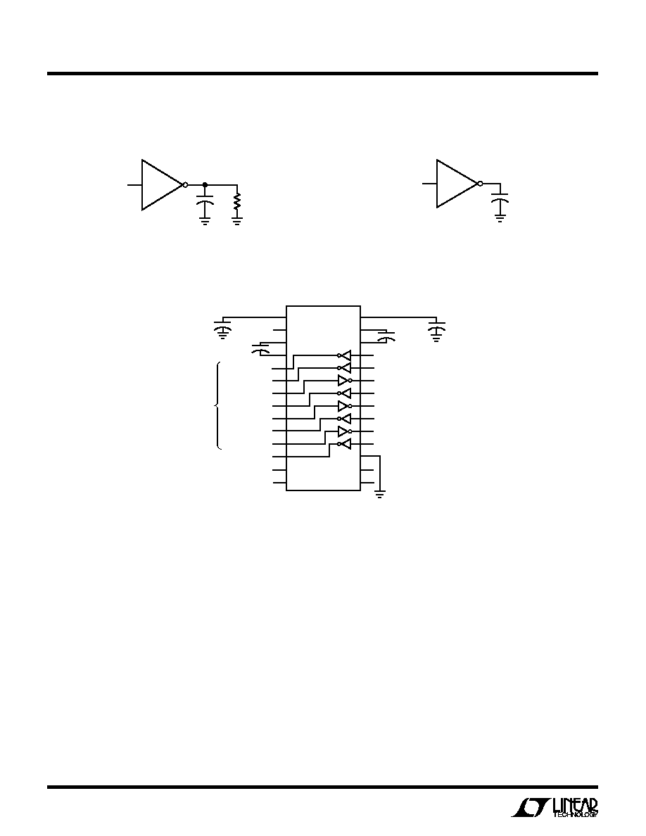
TEST CIRCUITS
Driver Timing Test Load
Receiver Timing Test Load
RX
RX INPUT
51pF
RX
OUTPUT
LTC1338 ∑ F04
DRIVER
DRIVER
INPUT
3k
51pF
DRIVER
OUTPUT
LTC1338 ∑ F03
ESD Test Circuit
LTC1338 ∑ TC01
V
CC
C1
0.1
µ
F
LTC1338
1
2
3
4
5
6
7
8
9
10
11
12
13
14
DRIVER 1 OUT
DRIVER 2 OUT
RX1 IN
DRIVER 3 OUT
RX2 IN
DRIVER 4 OUT
RX3 IN
DRIVER 5 OUT
RX ENABLE
NC
28
27
26
25
24
23
22
21
20
19
18
17
16
15
C3
0.1
µ
F
DRIVER 1 IN
DRIVER 2 IN
RX1 OUT
DRIVER 3 IN
RX2 OUT
DRIVER 4 IN
RX3 OUT
DRIVER 5 IN
GND
DRIVER ENABLE
NC
V
≠
V
+
C2
0.1
µ
F
C4
0.1
µ
F
RS232
LINE PINS
PROTECTED
TO ±10kV
7
LTC1338
Information furnished by Linear Technology Corporation is believed to be accurate and reliable.
However, no responsibility is assumed for its use. Linear Technology Corporation makes no represen-
tation that the interconnection of its circuits as described herein will not infringe on existing patent rights.
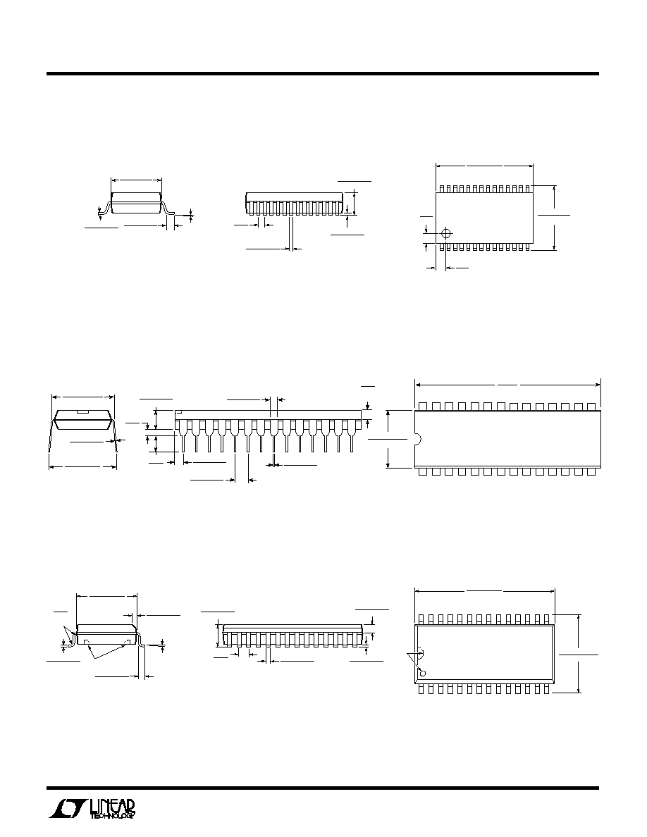
0∞ ≠ 8∞ TYP
NOTE 1
0.009 ≠ 0.013
(0.229 ≠ 0.330)
0.016 ≠ 0.050
(0.406 ≠ 1.270)
0.291 ≠ 0.299
(7.391 ≠ 7.595)
(NOTE 2)
◊
45
∞
0.010 ≠ 0.029
(0.254 ≠ 0.737)
0.005
(0.127)
RAD MIN
0.037 ≠ 0.045
(0.940 ≠ 1.143)
0.004 ≠ 0.012
(0.102 ≠ 0.305)
0.093 ≠ 0.104
(2.362 ≠ 2.642)
0.050
(1.270)
TYP
0.014 ≠ 0.019
(0.356 ≠ 0.482)
NOTE 1
0.697 ≠ 0.712
(17.70 ≠ 18.08)
(NOTE 2)
0.394 ≠ 0.419
(10.007 ≠ 10.643)
1
2
3
4
5
6
7
8
9 10 11 12
14
13
25
26
22 21 20 19 18 17 16 15
23
24
27
28
NOTE:
1. PIN 1 IDENT, NOTCH ON TOP AND CAVITIES ON THE BOTTOM OF PACKAGES ARE THE MANUFACTURING OPTIONS.
THE PART MAY BE SUPPLIED WITH OR WITHOUT ANY OF THE OPTIONS.
2. THESE DIMENSIONS DO NOT INCLUDE MOLD FLASH OR PROTRUSIONS.
MOLD FLASH OR PROTRUSIONS SHALL NOT EXCEED 0.006 INCH (0.15mm).
S Package
28-Lead SOL
PACKAGE DESCRIPTIO
U
Dimensions in inches (millimeters) unless otherwise noted.
G Package
28-Lead SSOP
0.301 ≠ 0.311
(7.65 ≠ 7.90)
1 2 3 4 5 6 7 8 9 10 11 12
14
13
0.397 ≠ 0.407*
(10.07 ≠ 10.33)
25
26
22 21 20 19 18 17 16 15
23
24
27
28
0.045
(1.14)
0.045
(1.14)
0.068 ≠ 0.078
(1.73 ≠ 1.99)
0.002 ≠ 0.008
(0.05 ≠ 0.21)
0.0256
(0.65)
BSC
0.010 ≠ 0.015
(0.25 ≠ 0.38)
0.005 ≠ 0.009
(0.13 ≠ 0.22)
0∞ ≠ 8∞
0.022 ≠ 0.037
(0.55 ≠ 0.95)
0.205 ≠ 0.212*
(5.20 ≠ 5.38)
*THESE DIMENSIONS DO NOT INCLUDE MOLD FLASH OR PROTRUSIONS.
MOLD FLASH OR PROTRUSIONS SHALL NOT EXCEED 0.006 INCH (0.15mm).
N Package
28-Lead Plastic DIP
0.505 ≠ 0.560
(12.827 ≠ 14.224)
1.455
(36.957)
MAX
1
2
3
4
5
6
7
8
9
10
27
19
20
21
22
24
23
25
26
28
11
12
13
14
15
16
17
18
0.009 ≠ 0.015
(0.229 ≠ 0.381)
0.625
+0.025
≠0.015
+0.635
≠0.381
15.87
(
)
0.600 ≠ 0.625
(15.240 ≠ 15.875)
0.070
(1.778)
TYP
0.015
(0.381)
MIN
0.125
(3.175)
MIN
0.130 ± 0.005
(3.302 ± 0.127)
0.018 ± 0.003
(0.457 ± 0.076)
0.035 ≠ 0.080
(0.889 ≠ 2.032)
0.100 ± 0.010
(2.540 ± 0.254)
0.045 ≠ 0.065
(1.143 ≠ 1.651)

8
LTC1338
Linear Technology Corporation
1630 McCarthy Blvd., Milpitas, CA 95035-7487
(408) 432-1900
q
FAX
: (408) 434-0507
q
TELEX
: 499-3977
©
LINEAR TECHNOLOGY CORPORATION 1993
LT/GP 1093 10K REV 0 ∑ PRINTED IN USA
NORTHEAST REGION
Linear Technology Corporation
One Oxford Valley
2300 E. Lincoln Hwy.,Suite 306
Langhorne, PA 19047
Phone: (215) 757-8578
FAX: (215) 757-5631
Linear Technology Corporation
266 Lowell St., Suite B-8
Wilmington, MA 01887
Phone: (508) 658-3881
FAX: (508) 658-2701
U.S. Area Sales Offices
SOUTHEAST REGION
Linear Technology Corporation
17060 Dallas Parkway
Suite 208
Dallas, TX 75248
Phone: (214) 733-3071
FAX: (214) 380-5138
CENTRAL REGION
Linear Technology Corporation
Chesapeake Square
229 Mitchell Court, Suite A-25
Addison, IL 60101
Phone: (708) 620-6910
FAX: (708) 620-6977
SOUTHWEST REGION
Linear Technology Corporation
22141 Ventura Blvd.
Suite 206
Woodland Hills, CA 91364
Phone: (818) 703-0835
FAX: (818) 703-0517
NORTHWEST REGION
Linear Technology Corporation
782 Sycamore Dr.
Milpitas, CA 95035
Phone: (408) 428-2050
FAX: (408) 432-6331
FRANCE
Linear Technology S.A.R.L.
Immeuble "Le Quartz"
58 Chemin de la Justice
92290 Chatenay Malabry
France
Phone: 33-1-41079555
FAX: 33-1-46314613
GERMANY
Linear Techonolgy GMBH
Untere Hauptstr. 9
D-85386 Eching
Germany
Phone: 49-89-3197410
FAX: 49-89-3194821
JAPAN
Linear Technology KK
5F YZ Bldg.
4-4-12 Iidabashi, Chiyoda-Ku
Tokyo, 102 Japan
Phone: 81-3-3237-7891
FAX: 81-3-3237-8010
TAIWAN
Linear Technology Corporation
Rm. 801, No. 46, Sec. 2
Chung Shan N. Rd.
Taipei, Taiwan, R.O.C.
Phone: 886-2-521-7575
FAX: 886-2-562-2285
UNITED KINGDOM
Linear Technology (UK) Ltd.
The Coliseum, Riverside Way
Camberley, Surrey GU15 3YL
United Kingdom
Phone: 44-276-677676
FAX: 44-276-64851
KOREA
Linear Technology Korea Branch
Namsong Building, #505
Itaewon-Dong 260-199
Yongsan-Ku, Seoul
Korea
Phone: 82-2-792-1617
FAX: 82-2-792-1619
SINGAPORE
Linear Technology Pte. Ltd.
101 Boon Keng Road
#02-15 Kallang Ind. Estates
Singapore 1233
Phone: 65-293-5322
FAX: 65-292-0398
World Headquarters
Linear Technology Corporation
1630 McCarthy Blvd.
Milpitas, CA 95035-7487
Phone: (408) 432-1900
FAX: (408) 434-0507
08/16/93
International Sales Offices