 | ÐлекÑÑоннÑй компоненÑ: LTC1340 | СкаÑаÑÑ:  PDF PDF  ZIP ZIP |
Äîêóìåíòàöèÿ è îïèñàíèÿ www.docs.chipfind.ru
1
LTC1340
Low Noise, Voltage-Boosted
Varactor Driver
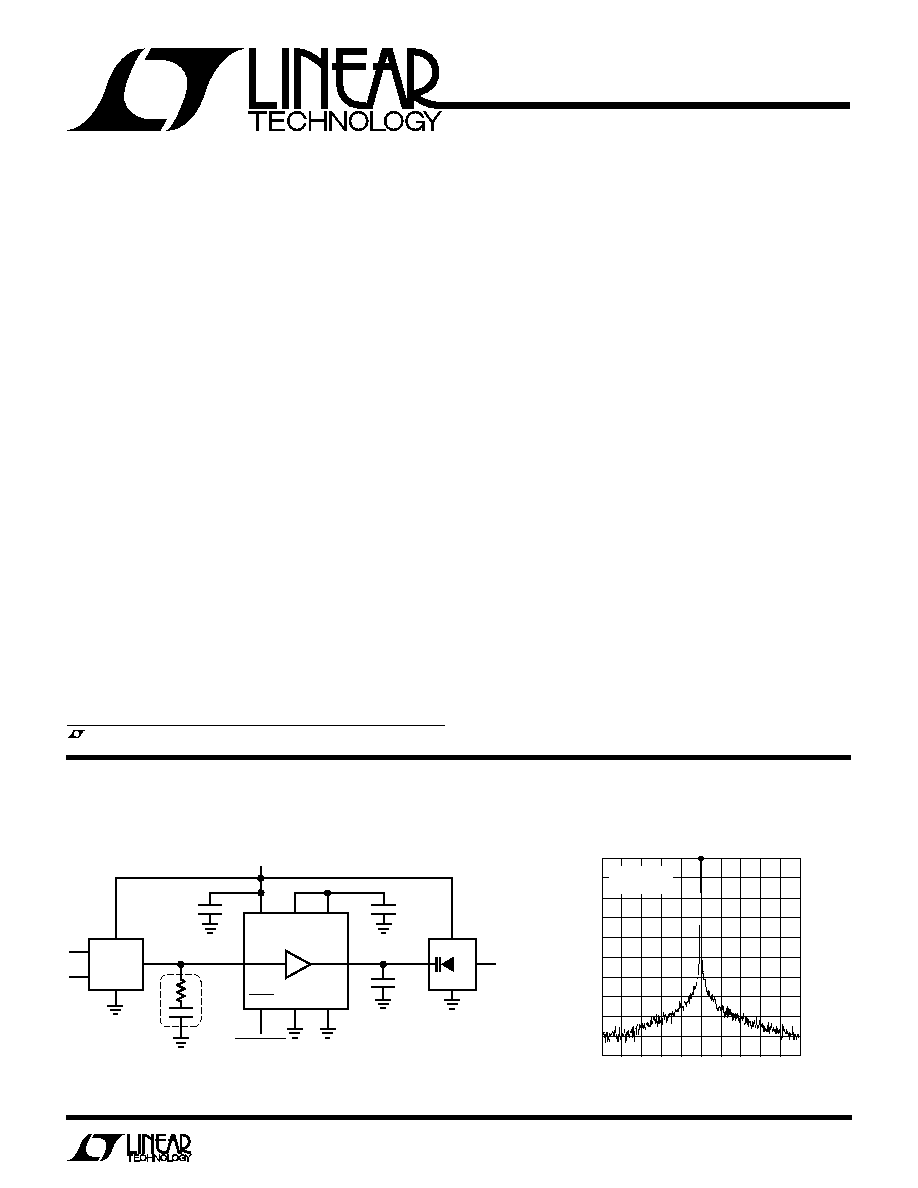
FREQUENCY (120kHz/DIV)
0dB
RELATIVE POWER (10dB/DIV)
1340 TA02
900MHz
V
CC
= 3V
C
OUT
= 270pF
Spectral Plot of VCO Output Driven by LTC1340
Resolution Bandwidth = 300Hz
DESCRIPTIO
N
U
FEATURES
The LTC
®
1340 is a varactor diode driver designed to generate
5V varactor drive from a single 3V or higher voltage supply.
It includes a low noise amplifier with an internal gain of 2.3
and a self-contained charge pump to generate output volt-
ages above the input supply. The amplifier input stage
includes a built-in offset voltage that allows the output voltage
to swing to ground without requiring OV on the input. This
feature maintains the phase detector within its linear range of
operation. The LTC1340 requires only three external surface
mount capacitors to implement a complete varactor driver
module.
The LTC1340 features output referred noise of 15
µ
V
RMS
,
minimizing frequency deviation in PLL frequency synthe-
sizer systems. Supply current is 400
µ
A typically with a 3V
supply, and drops to 1
µ
A in shutdown, maximizing operating
life in battery-powered systems. Amplifier bandwidth is user-
adjustable from 10kHz up to 500kHz and the output typically
sinks or sources 20
µ
A, allowing fast output signal changes
with a typical varactor load. The amplifier input features rail-
to-rail input common mode range, allowing it
to interface with the output of virtually any phase detector
circuit.
The LTC1340 is available in MS8 and SO-8 packages.
TYPICAL APPLICATIO
N
U
Low Voltage Frequency Synthesizer
LTC1340
PGND
CP
VCO
AV
CC
A
V
= 2.3
V
CC
0V TO 5V
IN
1
8
7
6
2
3
4
5
3V
1340 TA01
OUT
LOOP
FILTER
SHDN
SHUTDOWN
AGND
270pF
0.1
µ
F
0.1
µ
F
PHASE
DETECTOR
, LTC and LT are registered trademarks of Linear Technology Corporation.
s
Generates 5V Varactor Drive from a 3V Supply
s
Wide Supply Voltage Range: 2.7V to 6V
s
Requires Only Three External Components
s
Micropower Operation: 400
µ
A at 3V Supply
s
Shutdown Mode Drops Supply Current Below 1
µ
A
s
Low Output Noise: 15
µ
V
RMS
s
Amplifier Gain: 2.3
s
Up to 500kHz Signal Bandwidth
s
MS8 and SO-8 Packages
s
Very Low Input Bias Current: 10nA Max
s
Amplifier Offset Maintains Phase Detector
in Linear Region
APPLICATIO
N
S
U
s
5V Varactor Drive from a Single Li-Ion Cell
s
5V Varactor Drive from Three NiCd/NiMH Cells
s
Cellular Telephones
s
Portable RF Equipment
s
Radio Modems
s
Wireless Data Transmission
2
LTC1340
ABSOLUTE
M
AXI
M
U
M
RATINGS
W
W
W
U
Supply Voltage (V
CC
) ................................................. 7V
Input Voltage (AV
CC
) ............................................... 14V
Input Voltage (SHDN, IN) ............... 0.3V to V
CC
+ 0.3V
Output Voltage (CP, OUT) ............ 0.3V to AV
CC
+ 0.3V
Output Short-Circuit Duration .......................... Indefinite
Commercial Temperature Range ................. 0
°
C to 70
°
C
Extended Commercial Operating
Temperature Range (Note 1) ............. 40
°
C to 85
°
C
Storage Temperature Range ................. 65
°
C to 150
°
C
Lead Temperature (Soldering, 10 sec.) ................. 300
°
C
PACKAGE/ORDER I
N
FOR
M
ATIO
N
W
U
U
T
JMAX
= 125
°
C,
JA
= 200
°
C/ W
1
2
3
4
CP
V
CC
SHDN
PGND
8
7
6
5
AV
CC
OUT
AGND
IN
TOP VIEW
MS8 PACKAGE
8-LEAD PLASTIC MSOP
LTC1340CMS8
ORDER PART
NUMBER
ORDER PART
NUMBER
LTC1340CS8
MS8 PART MARKING
S8 PART MARKING
LTBM
1340
AV
CC
OUT
AGND
IN
CP
V
CC
SHDN
PGND
S8 PACKAGE
8-LEAD PLASTIC SO
TOP VIEW
1
2
3
4
8
7
6
5
T
JMAX
= 125
°
C,
JA
= 130
°
C/ W
Consult factory for Industrial and Military grade parts.
SYMBOL PARAMETER
CONDITIONS
MIN
TYP
MAX
UNITS
V
CC
Input Supply Voltage
q
2.7
6
V
I
CC
Supply Current
I
OUT
= 0, 2.7V
V
CC
6V
q
500
900
µ
A
Shutdown, 2.7V
V
CC
6V
q
1
10
µ
A
V
OL
Low Output Voltage Swing
V
CC
= 2.7V, 6V,
I
OUT
= 0
µ
A
q
0.25
V
V
CC
= 2.7V, 6V,
I
OUT
= 14
µ
A
q
0.6
V
V
OH
High Output Voltage Swing
V
CC
= 2.7V,
I
OUT
= 0
µ
A
q
4.6
V
V
CC
= 6V,
I
OUT
= 0
µ
A
q
10.5
V
V
CC
= 2.7V,
I
OUT
= 14
µ
A
q
4.25
V
V
CC
= 6V,
I
OUT
= 14
µ
A
q
9.75
V
I
OUT
Output Sink/Source Current
0.6V
V
OUT
4.25V, V
CC
= 2.7V
q
±
14
±
20
±
35
µ
A
0.6V
V
OUT
9.75V, V
CC
= 6V
q
±
14
±
20
±
35
µ
A
t
OUT
Output Transition Time
C
OUT
= 1nF,
V
OUT
=
±
4V
q
200
285
µ
s
V
IN
Input Voltage Range
q
0
V
CC
V
I
B
Input Bias Current
0.1V
V
IN
V
CC
±
0.01
±
1
nA
q
±
10
nA
V
OS
Input Offset Voltage
q
0.15
0.35
0.60
V
A
V
Amplifier Gain
V
IN
= 1V, AV
CC
= 5V
q
2.1
2.3
2.5
V/V
g
m
Amplifier Transconductance
V
OUT
= 2.5V, AV
CC
= 5V
1200
1800
2300
µ
mho
V
OUT
= 2.5V, AV
CC
= 5V
q
800
3200
µ
mho
R
OUT
Output Impedance
V
OUT
= 1/2AV
CC
1
M
e
n
Output Noise Voltage
1kHz to 100kHz, C
OUT
= 1nF
15
25
µ
V
RMS
BW
3dB Signal Bandwidth
C
OUT
= 1nF
125
kHz
PSRR
Power Supply Rejection Ratio
AV
CC
= 4V to 6V, C
OUT
= 1nF
q
60
90
dB
I
SHDN
Shutdown Logic Input Current
0.1V
V
SHDN
V
CC
±
0.01
±
1
µ
A
ELECTRICAL CHARACTERISTICS
T
A
= 25
°
C, unless otherwise noted. (Note 1)
3
LTC1340
ELECTRICAL CHARACTERISTICS
SYMBOL PARAMETER
CONDITIONS
MIN
TYP
MAX
UNITS
t
START
Charge Pump Start-Up Time
C
CP
= 0.1
µ
F, V
CC
= 2.7V, I
OUT
= 0
q
1.2
5
ms
V
RIPPLE
Charge Pump Output Ripple at C
P
C
CP
= C
VCC
= 0.1
µ
F, V
CC
= 2.7V, I
OUT
= 0 (Note 2)
200
µ
V
P-P
f
CP
Charge Pump Frequency
(Note 3)
q
2.5
4
MHz
The
q
denotes specifications which apply over the specified temperature
range.
Note 1: C grade device specifications are guaranteed over the 0
°
C to 70
°
C
temperature range. In addition, C grade device specifications are assured
over the 40
°
C to 85
°
C temperature range by design or correlation, but
are not production tested.
T
A
= 25
°
C, unless otherwise noted. (Note 1)
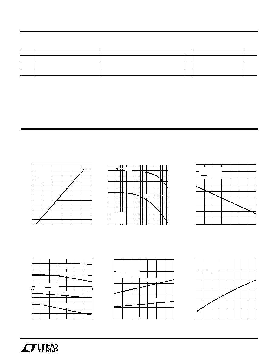
OUTPUT HIGH VOLTAGE (V)
9.4
9.3
9.2
9.1
9.0
8.9
4.9
4.8
4.7
4.6
4.5
4.4
1340 G04
TEMPERATURE (
°
C)
50
0
25
25
50
75
100
125
C
OUT
= 1nF
V
IN
= V
SHDN
= V
CC
I
OH
= 0, V
CC
= 5V
I
OH
= 0, V
CC
= 2.7V
I
OH
= 14
µ
A, V
CC
= 5V
I
OH
= 14
µ
A, V
CC
= 2.7V
Output High Voltage vs
Temperature
OUTPUT LOW VOLTAGE (V)
0.5
0.4
0.3
0.2
0.1
0
1340 G05
TEMPERATURE (
°
C)
50
0
25
25
50
75
100
125
V
CC
= 2.7V OR 5V
C
OUT
= 1nF
V
IN
= 0V
V
SHDN
= V
CC
I
OL
= 14
µ
A
I
OL
= 0
SUPPLY VOLTAGE (V)
2.5
TRANSCONDUCTANCE (
µ
mho)
3.5
3.0
4.5
4.0
5.5
6.0
5.0
6.5
1340 G06
2100
2050
2000
1950
1900
1850
1800
T
A
= 25
°
C
V
OUT
= 1/2AV
CC
V
SHDN
= V
CC
DC Transfer Curve
INPUT VOLTAGE (V)
0
OUTPUT VOLTAGE (V)
12
11
10
9
8
7
6
5
4
3
2
1
0
1
2
3
4
1340 G01
5
6
V
CC
= 2.7V
V
CC
= 5V
T
A
= 25
°
C
C
OUT
= 1nF
I
OUT
= 0
V
SHDN
= V
CC
V
CC
= 6V
TEMPERATURE (
°
C)
50
INPUT OFFSET VOLTAGE (V)
0
0.60
0.55
0.50
0.45
0.40
0.35
0.30
0.25
0.20
0.15
1340 G03
25
25
50
75
100
125
V
CC
= 2.7V TO 6V
C
OUT
= 1nF
V
SHDN
= V
CC
FREQUENCY (kHz)
1
VOLTAGE GAIN (dB)
PHASE SHIFT (DEG)
20
10
0
10
20
30
40
50
60
70
80
90
180
144
108
72
36
0
36
72
108
144
180
216
10
100
1000
1340 G02
V
CC
= 2.7V
T
A
= 25
°
C
C
OUT
= 1nF
PHASE
GAIN
Gain and Phase Shift vs
Frequency
TYPICAL PERFOR
M
A
N
CE CHARACTERISTICS
U
W
Input Offset Voltage vs
Temperature
Output Low Voltage vs
Temperature
Transconductance vs
Supply Voltage
Note 2: The charge pump output ripple is not tested but is correlated with
a PCB ground plane and high quality, low ESR, low ESL metalized
polyester 0.1
µ
F capacitors.
Note 3: The internal oscillator typically runs at 2MHz, but the charge pump
refreshes the output on both phases of the clock, resulting in an effective
4MHz operating frequency.
4
LTC1340
TRANSCONDUCTANCE (
µ
mho)
3000
2800
2600
2400
2200
2000
1800
1600
1400
1200
1000
1340 G07
TEMPERATURE (
°
C)
50
0
25
25
50
75
100
125
V
CC
= 6V
V
OUT
= 1/2AV
CC
V
SHDN
= V
CC
V
CC
= 5V
V
CC
= 2.7V
TYPICAL PERFOR
M
A
N
CE CHARACTERISTICS
U
W
TEMPERATURE (
°
C)
50
SUPPLY CURRENT (
µ
A)
0
700
650
600
550
500
450
400
350
300
1340 G09
25
25
50
75
100
125
V
SHDN
= V
CC
V
CC
= 6V
V
CC
= 5V
V
CC
= 2.7V
Supply Current vs Temperature
Transconductance vs
Temperature
GSM 900 MS Spectrum Due to
Modulation
FREQUENCY FROM THE CARRIER(kHz)
0
66
RELATIVE POWER (dB)
10
0
10
20
30
40
50
60
80
90
400
1200 1800
1340 G10
200
600
3000 6000
70
MEASUREMENT
BANDWIDTH
30kHz
MEASUREMENT
BANDWIDTH
100kHz
DATA TAKEN ON
LTC DEMO BOARD DC152
LTC1340
SUPPLY VOLTAGE (V)
2.5
SUPPLY CURRENT (
µ
A)
3.5
3.0
4.5
4.0
5.5
6.0
5.0
6.5
1340 G08
900
800
700
600
500
400
300
200
T
A
= 25
°
C
V
SHDN
= V
CC
Supply Current vs Supply Voltage
Rail-to-Rail Step Response at
V
CC
= 2.7V
V
IN
= 0.3V TO 2.6V
C
OUT
= 1nF
1340 G15
0V
10000
1000
100
10
1
1340 G12
INPUT BIAS CURRENT (pA)
TEMPERATURE (
°
C)
50
0
25
25
50
75
100
125
V
IN
= V
SHDN
= V
CC
= 5V
OUTPUT VOLTAGE NOISE (
µ
V/
RMS
)
25.0
22.5
20.0
17.5
15.0
12.5
10.0
7.50
5.0
1.50
0
1340 G11
TEMPERATURE (
°
C)
50
0
25
25
50
75
100
125
AV
CC
= 5V
C
OUT
= 1nF
Output Voltage Noise vs
Temperature
Input Bias Current vs
Temperature
TEMPERATURE (
°
C)
50
SHUTDOWN INPUT THRESHOLD (V)
0
2.4
2.2
2.0
1.8
1.6
1.4
1.2
1.0
0.8
1340 G13
25
25
50
75
100
125
V
CC
= 6V
V
CC
= 5V
V
CC
= 4V
V
CC
= 3V
V
CC
= 2.7V
Shutdown Input Threshold vs
Temperature
Rail-to-Rail Step Response at
V
CC
= 6V
0V
V
IN
= 0.3V TO 6V
C
OUT
= 1nF
1340 G14
5
LTC1340
PI
N
FU
N
CTIO
N
S
U
U
U
IN (Pin 5): Signal Input. The internal amplifier amplifies
the signal input at this pin typically by 2.3 to the OUT pin.
IN accepts signals from GND to V
CC
without phase rever-
sal or unusual behavior, allowing a direct connection to the
output of virtually any phase detector or loop filter pow-
ered from V
CC
.
AGND (Pin 6): Signal Ground. Connect AGND to the
ground plane in close proximity to the VCO ground. There
is an internal parasitic resistance of 50
between AGND
and PGND.
OUT (Pin 7): Driver Output. OUT is the output of the
internal g
m
amplifier and the internal feedback network. It
swings from GND to AV
CC
, and drives a varactor load
directly. The OUT pin requires an external capacitor
(
220pF) to AGND to ensure stability. OUT typically sinks
or sources 20
µ
A.
AV
CC
(Pin 8): Amplifier Supply. LTC recommends a direct
connection from AV
CC
to CP and also recommends a 0.1
µ
F
filter capacitor from CP to PGND.
CP (Pin 1): Charge Pump Output. This is the output of the
internal charge pump. The voltage at CP is nominally twice
the V
CC
input voltage. Connect CP to an external 0.1
µ
F
filter capacitor and AV
CC
.
V
CC
(Pin 2): Supply Input. This is the input supply to the
charge pump. V
CC
can range from 2.7V to 6V and requires
a 0.1
µ
F bypass capacitor to PGND.
SHDN (Pin 3) Shutdown. If SHDN is high (>V
CC
0.5V),
the LTC1340 operates normally. If SHDN is pulled low
(< 0.5V), the LTC1340 enters shutdown mode and the
supply current drops to less than 1
µ
A typically. In shut-
down, the charge pump output voltage collapses and the
OUT pin enters a high impedance state. If SHDN returns
high, the charge pump output requires 1.2ms typically to
resume full voltage.
PGND (Pin 4): Power Ground. This is the charge pump
ground. Connect PGND to the system power supply
return.
FREQUENCY (MHz)
4.0
3.8
3.6
3.4
3.2
3.0
1340 G16
TEMPERATURE (
°
C)
50
0
25
25
50
75
100
125
V
SHDN
= V
CC
V
CC
= 6V
V
CC
= 2.7V
V
CC
= 5V
Charge Pump Frequency vs
Temperature
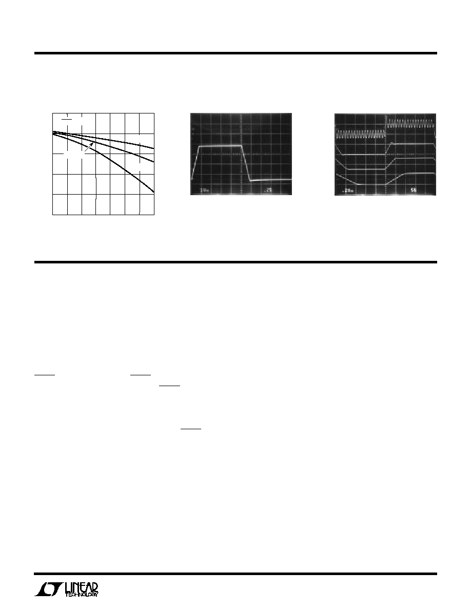
Small-Signal Response
1340 G18
C
OUT
= 220pF
C
OUT
= 470pF
C
OUT
= 1nF
C
OUT
= 0pF
TYPICAL PERFOR
M
A
N
CE CHARACTERISTICS
U
W
Large-Signal Response
V
IN
= 0.5V TO 2V
V
CC
= 2.7V
C
OUT
= 1nF
1340 G17
0V