Äîêóìåíòàöèÿ è îïèñàíèÿ www.docs.chipfind.ru
1
LTC1344A
Software-Selectable
Cable Terminator
Daisy-Chained Control Outputs
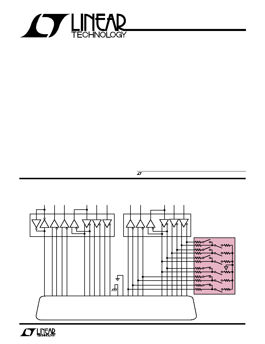
TYPICAL APPLICATIO
N
U
DTE or DCE Multiprotocol Serial Interface with DB-25 Connector
D2
D1
LTC1544
RTS
DTR
DSR
DCD
CTS
D3
R2
R1
R4
R3
D2
LTC1543
LL
TXD
SCTE
TXC
RXC
RXD
2
14
24
11
15
12
17
9
3
1
4
19
20
6
23
22
5
13
8
10
18
7
16
1344A TA01
LTC1344A
D3
R2
R1
R3
D1
TXD A (103)
TXD B
SCTE A (113)
SCTE B
RXC A (115)
RXC B
RXD A (104)
RXD B
RTS A (105)
RTS B
DTR A (108)
DTR B
CTS A (106)
CTS B
LL A (141)
SG (102)
SHIELD (101)
DB-25 CONNECTOR
TXC A (114)
TXC B
DCD A (107)
DCD B
DSR A (109)
DSR B
D4
s
Data Networking
s
CSU and DSU
s
Data Routers
APPLICATIO
N
S
U
, LTC and LT are registered trademarks of Linear Technology Corporation.
FEATURES
s
Software-Selectable Cable Termination for:
RS232 (V.28)
RS423 (V.10)
RS422 (V.11)
RS485
RS449
EIA530
EIA530-A
V.35
V.36
X.21
s
Outputs Won't Load the Line with Power Off
The LTC
®
1344A features six software-selectable
multiprotocol cable terminators. Each terminator can be
configured as an RS422 (V.11) 100
minimum differen-
tial load, V.35 T-network load or an open circuit for use
with RS232 (V.28) or RS423 (V.10) transceivers that
provide their own termination. When combined with the
LTC1543 and LTC1544, the LTC1344A forms a complete
software-selectable multiprotocol serial port. A data bus
latch feature allows sharing of the select lines between
multiple interface ports.
The LTC1344A is similar to the LTC1344 except for a
difference in the Mode Selection table.
The LTC1344A is available in a 24-lead SSOP.
DESCRIPTIO
N
U
2
LTC1344A
ABSOLUTE
M
AXI
M
U
M
RATINGS
W
W
W
U
W
U
U
PACKAGE/ORDER I FOR ATIO
ORDER PART
NUMBER
LTC1344ACG
LTC1344AIG
1
2
3
4
5
6
7
8
9
10
11
12
TOP VIEW
G PACKAGE
24-LEAD PLASTIC SSOP
24
23
22
21
20
19
18
17
16
15
14
13
M0
V
EE
R1C
R1B
R1A
R2A
R2B
R2C
R3A
R3B
R3C
GND
M1
M2
DCE/DTE
LATCH
R6B
R6A
R5A
R5B
R4A
R4B
V
CC
GND
T
JMAX
= 150
°
C,
JA
= 100
°
C/W
Consult factory for Military grade parts.
ELECTRICAL CHARACTERISTICS
V
CC
= 5V
±
5%, V
EE
= 5V
±
5%, T
A
= T
MIN
to T
MAX
(Notes 2, 3) unless otherwise noted.
(Note 1)
Positive Supply Voltage (V
CC
) ................................... 7V
Negative Supply Voltage (V
EE
) ........................... 13.2V
Input Voltage
(Logic Inputs) .................... (V
EE
0.3V) to (V
CC
+ 0.3V)
Input Voltage (Load Inputs) ..................................
±
18V
Power Dissipation .............................................. 600mW
Operating Temperature Range
LTC1344AC ............................................ 0
°
C to 70
°
C
LTC1344AI ......................................... 40
°
C to 85
°
C
Storage Temperature Range ................ 65
°
C to 150
°
C
Lead Temperature (Soldering, 10 sec)................. 300
°
C
Note 2: All currents into device pins are positive; all currents out of device
pins are negative. All voltages are reference to ground unless otherwise
specified.
Note 3: All typicals are given at V
CC
= 5V, V
EE
= 5V, T
A
= 25
°
C.
The
q
denotes specifications which apply over the full operating
temperature range.
Note 1: Absolute Maximum Ratings are those values beyond which the life
of a device may be impaired.
SYMBOL
PARAMETER
CONDITIONS
MIN
TYP
MAX
UNITS
Supplies
I
CC
Supply Current
All Digital Pins = GND or V
CC
q
0.4
1.0
mA
Terminator Pins
R
V.35
Differential Mode Impedance
All Loads (Figure 1), 2V
V
CM
2V (Commercial)
q
90
104
110
Common Mode Impedance
All Loads (Figure 2), 2V
V
CM
2V (Commercial)
q
135
153
165
All Loads (Figure 1), 2V
V
CM
2V (Industrial)
q
90
104
115
All Loads (Figure 2), 2V
V
CM
2V (Industrial)
q
130
153
170
R
V.11
Differential Mode Impedance
All Loads (Figure 1), V
CM
= 0V (Commercial)
q
100
104
110
All Loads (Figure 1), 7V
V
CM
7V (Commercial)
100
104
All Loads (Figure 1), V
CM
= 0V (Industrial)
q
95
104
115
All Loads (Figure 1), 7V
V
CM
7V (Industrial)
100
104
I
LEAK
High Impedance Leakage Current
All Loads, 7V
V
CM
7V
q
±
1
±
50
µ
A
Logic Inputs
V
IH
Input High Voltage
All Logic Input Pins
q
2
V
V
IL
Input Low Voltage
All Logic Input Pins
q
0.8
V
I
IN
Input Current
All Logic Input Pins
q
±
10
µ
A
3
LTC1344A
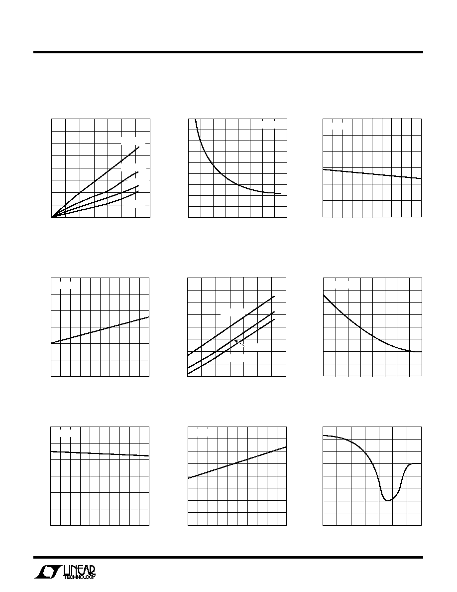
TYPICAL PERFOR
M
A
N
CE CHARACTERISTICS
U
W
V.11 or V.35 Differential Mode
Impedance vs Common Mode
Voltage
TEMPERATURE (
°
C)
40
DIFFERENTIAL MODE IMPEDANCE (
)
20
1344 G01
110
105
20
0
40
100
120
115
60
80
100
V
CM
= 7V
V
CM
= 2V
V
CM
= 0V
V
CM
= 7V
V
CC
VOLTAGE (V)
103
DIFFERENTIAL MODE IMPEDANCE (
)
104
105
1344 G03
4.6
4.8
5.0
5.2
5.4
T
A
= 25
°
C
COMMON MODE VOLTAGE (V)
8
DIFFERENTIAL MODE IMPEDANCE (
)
108
6
1344 G02
106
104
100
6
4
2
0
2
4
8
102
T
A
= 25
°
C
V.11 or V.35 Differential Mode
Impedance vs Temperature
V.35 Common Mode Impedance
vs Supply Voltage (V
CC
)
V.35 Common Mode Inpedance
vs Negative Supply Voltage (V
EE
)
V
CC
VOLTAGE (V)
151
COMMON MODE IMPEDANCE (
)
152
153
1344 G07
4.6
4.8
5.0
5.2
5.4
T
A
= 25
°
C
V
EE
VOLTAGE (V)
5.4
COMMON MODE IMPEDANCE (
)
153
154
4.6
1344 G08
152
151
150
5.2
5.0
4.8
T
A
= 25
°
C
Supply Current vs Temperature
TEMPERATURE (
°
C)
40
SUPPLY CURRENT (
µ
A)
500
420
340
260
180
20
1344 G09
20
0
40
60
80
100
V.11 or V.35 Differential Mode
Impedance vs Negative Supply
Voltage (V
EE
)
TEMPERATURE (
°
C)
40
COMMON MODE IMPEDANCE (
)
20
1344 G05
155
150
20
0
40
145
165
160
60
80
100
V
CM
= 2V
V
CM
= 2V
V
CM
= 0V
COMMON MODE VOLTAGE (V)
2
COMMON MODE IMPEDANCE (
)
154
156
2
1344 G06
152
150
1
0
1
158
T
A
= 25
°
C
V.35 Common Mode Impedance
vs Temperature
V.35 Common Mode Impedance
vs Common Mode Voltage
V
EE
VOLTAGE (V)
103
DIFFERENTIAL MODE IMPEDANCE (
)
104
105
1344 G04
5.4
5.2
5.0
4.8
4.6
T
A
= 25
°
C
V.11 or V.35 Differential Mode
Impedance vs Supply Voltage
(V
CC
)
4
LTC1344A
PI
N
FU
N
CTIO
N
S
U
U
U
M0 (Pin 1): TTL Level Mode Select Input. The data on M0
is latched when LATCH is high.
V
EE
(Pin 2): Negative Supply Voltage Input. Can connect
directly to the LTC1543 V
EE
pin. Connect a 1
µ
F capacitor
to ground.
R1C (Pin 3): Load 1 Center Tap.
R1B (Pin 4): Load 1 Node B.
R1A (Pin 5): Load 1 Node A.
R2A (Pin 6): Load 2 Node A.
R2B (Pin 7): Load 2 Node B.
R2C (Pin 8): Load 2 Center Tap.
R3A (Pin 9): Load 3 Node A.
R2B (Pin 10): Load 2 Node B.
R3C (Pin 11): Load 3 Center Tap.
GND (Pin 12): Ground Connection for Load 1 to Load 3.
GND (Pin 13): Ground Connection for Load 4 to Load 6.
V
CC
(Pin 14): Positive Supply Input. 4.75V
V
CC
5.25V.
R4B (Pin 15): Load 4 Node B.
R4A (Pin 16): Load 4 Node A.
R5B (Pin 17): Load 5 Node B.
R5A (Pin 18): Load 5 Node A.
R6A (Pin 19): Load 6 Node A.
R6B (Pin 20): Load 6 Node B.
LATCH (Pin 21): TTL Level Logic Signal Latch Input. When
LATCH is low the input buffers on M0, M1, M2 and DCE/
DTE are transparent. When LATCH is high the logic pins
are latched into their respective input buffers. The data
latch allows the select lines to be shared between multiple
I/O ports.
DCE/DTE (Pin 22): TTL Level Mode Select Input. DCE
mode is selected when high and DTE mode when low. The
data on DCE/DTE is latched when LATCH is high.
M2 (Pin 23): TTL Level Mode Select Input 1. The data on
M2 is latched when LATCH is high.
M1 (Pin 24): TTL Level Mode Select Input 2. The data on
M1 is latched when LATCH is high.
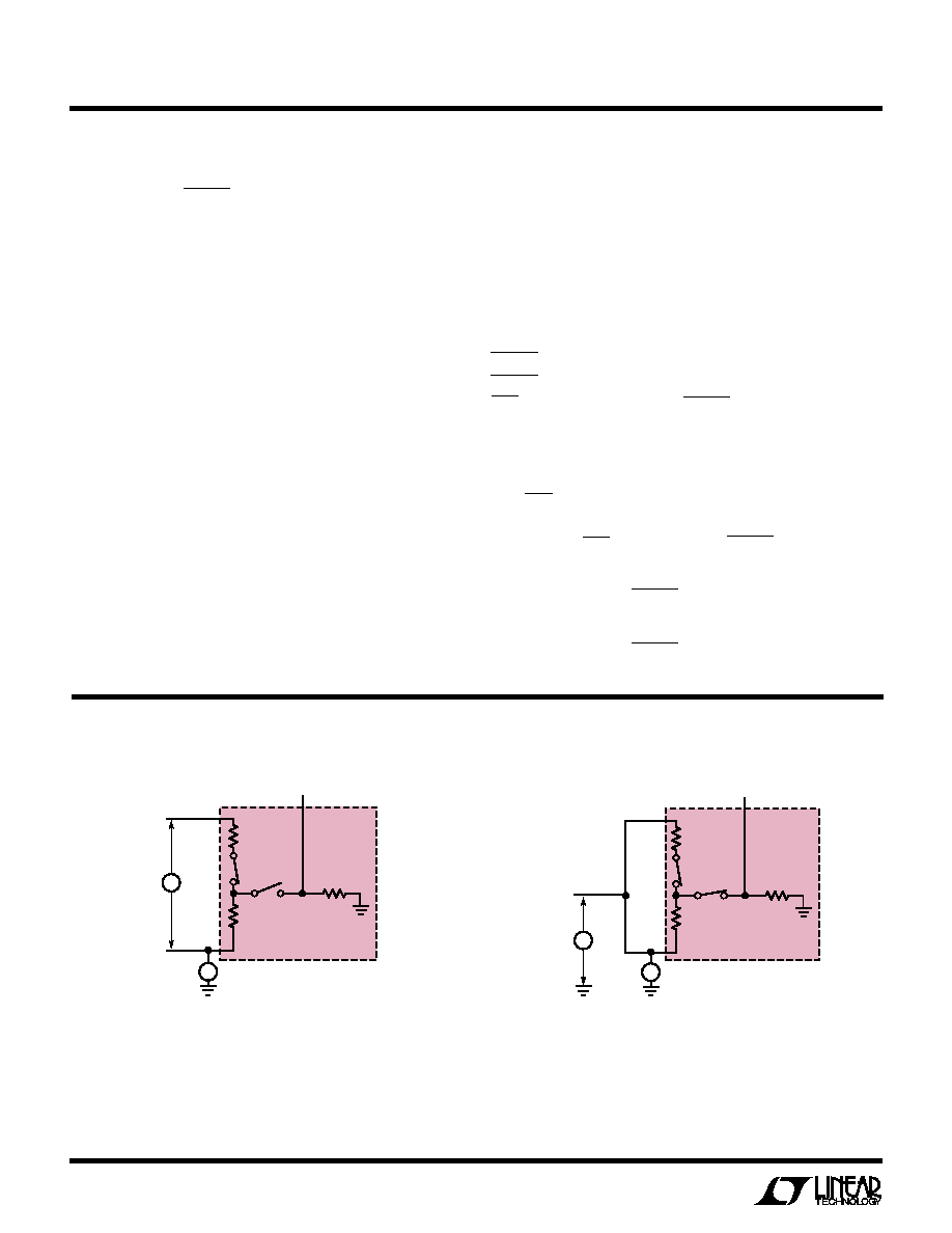
TEST CIRCUITS
R1
51.5
R2
51.5
±
2V
1344 F02
R3
124
S2
ON
S1
ON
C
V
A, B
LTC1344A
R1
51.5
R2
51.5
±
7V OR
±
2V
1344 F01
R3
124
S2
OFF
S1
ON
C
V
A
B
LTC1344A
Figure 2. V.35 Common Mode Impedance Measurement
Figure 1. Differential V.11 or V.35 Impedance Measurement
5
LTC1344A
LTC1344A
MODE NAME
DCE/DTE
M2
M1
M0
R1
R2
R3
R4
R5
R6
V.10/RS423
X
0
0
0
Z
Z
Z
Z
Z
Z
RS530A
0
0
0
1
Z
Z
Z
V.11
V.11
V.11
1
0
0
1
Z
Z
Z
Z
V.11
V.11
RS530
0
0
1
0
Z
Z
Z
V.11
V.11
V.11
1
0
1
0
Z
Z
Z
Z
V.11
V.11
X.21
0
0
1
1
Z
Z
Z
V.11
V.11
V.11
1
0
1
1
Z
Z
Z
Z
V.11
V.11
V.35
0
1
0
0
V.35
V.35
Z
V.35
V.35
V.35
1
1
0
0
V.35
V.35
V.35
Z
V.35
V.35
RS449/V.36
0
1
0
1
Z
Z
Z
V.11
V.11
V.11
1
1
0
1
Z
Z
Z
Z
V.11
V.11
V.28/RS232
X
1
1
0
Z
Z
Z
Z
Z
Z
No Cable
X
1
1
1
V.11
V.11
V.11
V.11
V.11
V.11
X = don't care, 0 = logic low, 1 = logic high
ODE SELECTIO
W U
R1
51.5
R2
51.5
R3
124
S2
OFF
S1
ON
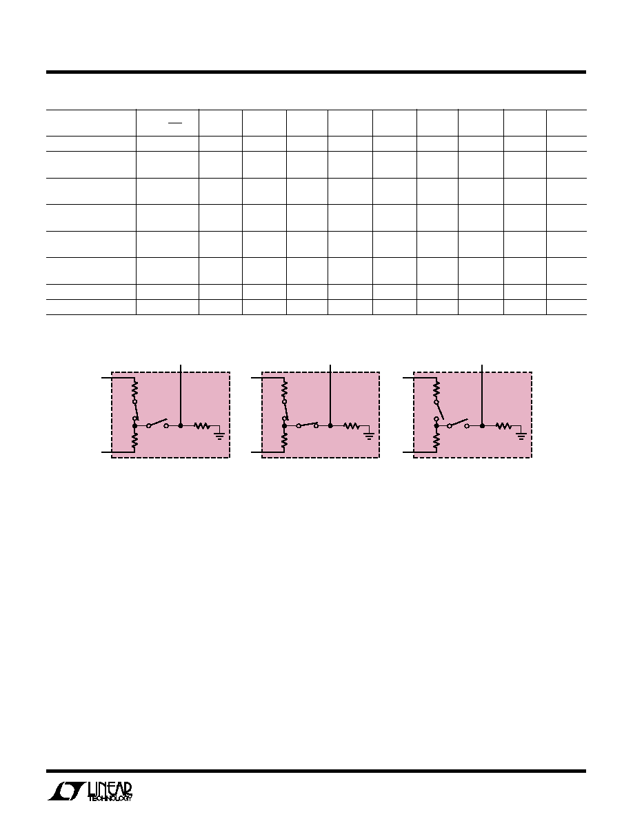
V.11 Mode
V.35 Mode
High-Z Mode
A
B
R1
51.5
R2
51.5
R3
124
S2
ON
S1
ON
A
B
R1
51.5
R2
51.5
1344 F03
R3
124
A
B
S2
OFF
S1
OFF
C
C
C
LTC1344A
LTC1344A
LTC1344A
Figure 3. LTC1344A Modes