 | –≠–ª–µ–∫—Ç—Ä–æ–Ω–Ω—ã–π –∫–æ–º–ø–æ–Ω–µ–Ω—Ç: LTC1344C | –°–∫–∞—á–∞—Ç—å:  PDF PDF  ZIP ZIP |
1
LTC1344
Software-Selectable
Cable Terminator
s
Software-Selectable Cable Termination for:
RS232 (V.28)
RS423 (V.10)
RS422 (V.11)
RS485
RS449
EIA530
EIA530-A
V.35
V.36
X.21
s
Outputs Won't Load the Line with Power Off
The LTC
Æ
1344 features six software-selectable
multiprotocol cable terminators. Each terminator can be
configured as an RS422 (V.11) 100
minimum differen-
tial load, V.35 T-network load or an open circuit for use
with RS232 (V.28) or RS423 (V.10) transceivers that
provide their own termination. When combined with the
LTC1343, the LTC1344 forms a complete software-select-
able multiprotocol serial port. A data bus latch feature
allows sharing of the select lines between multiple inter-
face ports.
The LTC1344 is available in a 24-lead SSOP.
Daisy-Chained Control Outputs
s
Data Networking
s
CSU and DSU
s
Data Routers
, LTC and LT are registered trademarks of Linear Technology Corporation.
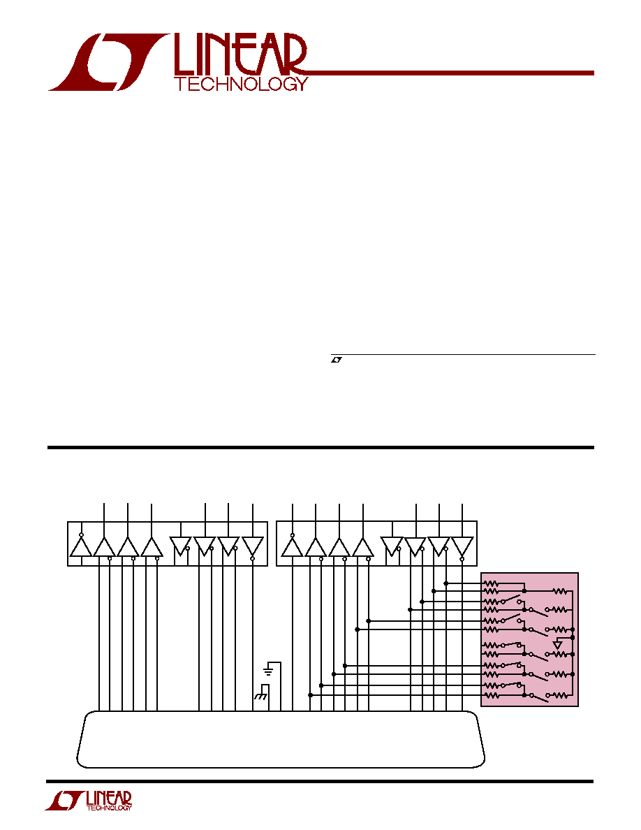
D2
LTC1343
RTS
DTR
DSR
DCD
CTS
RL
D1
D3
D4
R1
R3
R4
R2
D2
LTC1343
LL
TXD
SCTE
TXC
RXC
RXD
TM
LL A (141)
TXD A (103)
TXD B
SCTE A (113)
SCTE B
RXC A (115)
RXC B
RXD A (104)
RXD B
RTS A (105)
RTS B
DTR A (108)
DTR B
CTS A (106)
CTS B
TM A (142)
SGND (102)
SHIELD (101)
18
2
14
24
11
15
12
17
9
3
1
4
19
20
23
6
22
8
10
5
13
21
7
16
25
1344 TA01
DB-25 CONNECTOR
LTC1344
D1
D3
D4
R1
R3
R4
R2
TXC A (114)
TXC B
RL A (140)
DCD A (109)
DCD B
DSR A (107)
DSR B
FEATURES
DESCRIPTIO
U
APPLICATIO S
U
TYPICAL APPLICATIO
N
U
2
LTC1344
ABSOLUTE
M
AXI
M
U
M
RATINGS
W
W
W
U
W
U
U
PACKAGE/ORDER I FOR ATIO
ORDER PART
NUMBER
LTC1344CG
LTC1344IG
1
2
3
4
5
6
7
8
9
10
11
12
TOP VIEW
G PACKAGE
24-LEAD PLASTIC SSOP
24
23
22
21
20
19
18
17
16
15
14
13
M0
V
EE
R1C
R1B
R1A
R2A
R2B
R2C
R3A
R3B
R3C
GND
M1
M2
DCE/DTE
LATCH
R6B
R6A
R5A
R5B
R4A
R4B
V
CC
GND
T
JMAX
= 150
∞
C,
JA
= 100
∞
C/W
Consult factory for Military grade parts.
ELECTRICAL CHARACTERISTICS
The
q
denotes the specifications which apply over the full operating temperature range, otherwise specifications are at T
A
= 25
∞
.
V
CC
= 5V
±
5%, V
EE
= ≠5V
±
5%, T
A
= T
MIN
to T
MAX
(Notes 2, 3) unless otherwise noted.
SYMBOL
PARAMETER
CONDITIONS
MIN
TYP
MAX
UNITS
Supplies
I
CC
Supply Current
All Digital Pins = GND or V
CC
q
200
700
µ
A
Terminator Pins
R
V.35
Differential Mode Impedance
All Loads (Figure 1), ≠ 2V
V
CM
2V (Commercial)
q
90
103
110
Common Mode Impedance
All Loads (Figure 2), ≠ 2V
V
CM
2V (Commercial)
q
135
153
165
All Loads (Figure 1), ≠ 2V
V
CM
2V (Industrial)
q
90
104
125
All Loads (Figure 2), ≠ 2V
V
CM
2V (Industrial)
q
130
153
170
R
V.11
Differential Mode Impedance
All Loads (Figure 1), ≠ 7V
V
CM
7V (Commercial)
100
104
All Loads (Figure 1), V
CM
= 0V (Commercial)
q
100
104
110
All Loads (Figure 1), V
CM
= 0V (Industrial)
q
95
104
125
I
LEAK
High Impedance Leakage Current
All Loads, ≠ 7V
V
CM
7V (Commercial)
q
±
1
±
50
µ
A
Logic Inputs
V
IH
Input High Voltage
All Logic Input Pins
q
2
V
V
IL
Input Low Voltage
All Logic Input Pins
q
0.8
V
I
IN
Input Current
All Logic Input Pins
q
±
10
µ
A
Note 3: All typicals are given at V
CC
= 5V, V
EE
= ≠ 5V, T
A
= 25
∞
C.
Note 1: Absolute Maximum Ratings are those values beyond which the life
of a device may be impaired.
Note 2: All currents into device pins are positive; all currents out of device
pins are negative. All voltages are reference to ground unless otherwise
specified.
(Note 1)
Positive Supply Voltage (V
CC
) ................................... 7V
Negative Supply Voltage (V
EE
) ........................... ≠ 13.2V
Input Voltage (Logic Inputs) .... V
EE
≠ 0.3V to V
CC
+ 0.3V
Input Voltage (Load Inputs) ..................................
±
18V
Operating Temperature Range
LTC1344C ............................................... 0
∞
C to 70
∞
C
LTC1344I ........................................... ≠ 40
∞
C to 85
∞
C
Storage Temperature Range ................ ≠ 65
∞
C to 150
∞
C
Lead Temperature (Soldering, 10 sec)................. 300
∞
C
3
LTC1344
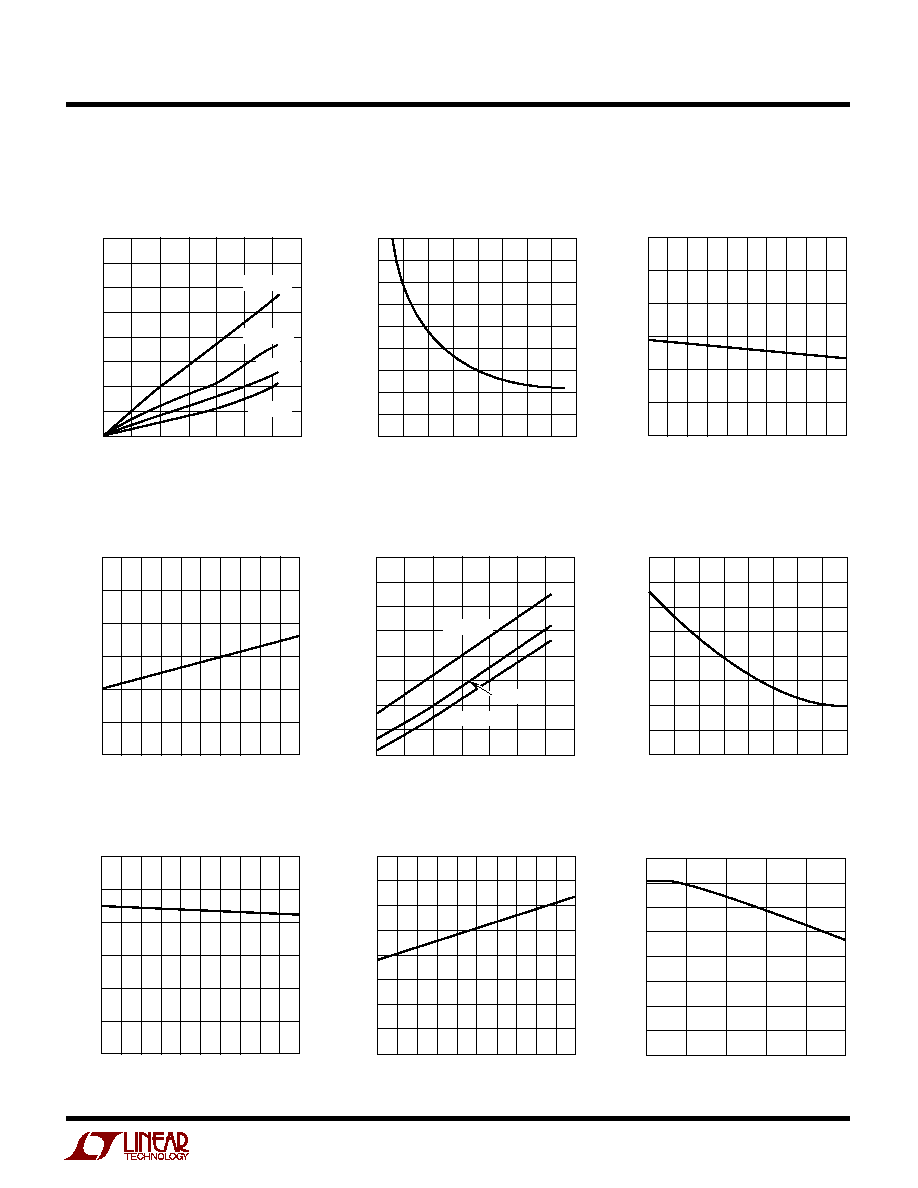
TYPICAL PERFOR
M
A
N
CE CHARACTERISTICS
U
W
V.11 or V.35 Differential Mode
Impedance vs Common Mode
Voltage
TEMPERATURE (
∞
C)
≠40
DIFFERENTIAL MODE IMPEDANCE (
)
20
1344 G01
110
105
≠20
0
40
100
120
115
60
80
100
V
CM
= ≠7V
V
CM
= ≠2V
V
CM
= 0V
V
CM
= 7V
V
CC
VOLTAGE (V)
103
DIFFERENTIAL MODE IMPEDANCE (
)
104
105
1344 G03
4.6
4.8
5.0
5.2
5.4
COMMON MODE VOLTAGE (V)
≠8
DIFFERENTIAL MODE IMPEDANCE (
)
108
6
1344 G02
106
104
100
≠ 6
≠ 4
≠2
0
2
4
8
102
V.11 or V.35 Differential Mode
Impedance vs Temperature
V.35 Common Mode Impedance
vs Supply Voltage (V
CC
)
V.35 Common Mode Inpedance
vs Negative Supply Voltage (V
EE
)
V
CC
VOLTAGE (V)
151
COMMON MODE IMPEDANCE (
)
152
153
1344 G07
4.6
4.8
5.0
5.2
5.4
V
EE
VOLTAGE (V)
≠ 5.4
COMMON MODE IMPEDANCE (
)
153
154
≠ 4.6
1344 G08
152
151
150
≠ 5.2
≠ 5.0
≠ 4.8
Supply Current vs Temperature
TEMPERATURE (
∞
C)
≠50
SUPPLY CURRENT (
µ
A)
1344 G09
310
290
270
250
230
210
190
170
150
≠20
10
40
70
100
V.11 or V.35 Differential Mode
Impedance vs Negative Supply
Voltage (V
EE
)
TEMPERATURE (
∞
C)
≠ 40
COMMON MODE IMPEDANCE (
)
20
1344 G05
155
150
≠20
0
40
145
165
160
60
80
100
V
CM
= ≠2V
V
CM
= 2V
V
CM
= 0V
COMMON MODE VOLTAGE (V)
≠2
COMMON MODE IMPEDANCE (
)
154
156
2
1344 G06
152
150
≠1
0
1
158
V.35 Common Mode Impedance
vs Temperature
V.35 Common Mode Impedance
vs Common Mode Voltage
V
EE
VOLTAGE (V)
103
DIFFERENTIAL MODE IMPEDANCE (
)
104
105
1344 G04
≠ 5.4
≠ 5.2
≠ 5.0
≠ 4.8
≠ 4.6
V.11 or V.35 Differential Mode
Impedance vs Supply Voltage
(V
CC
)
4
LTC1344
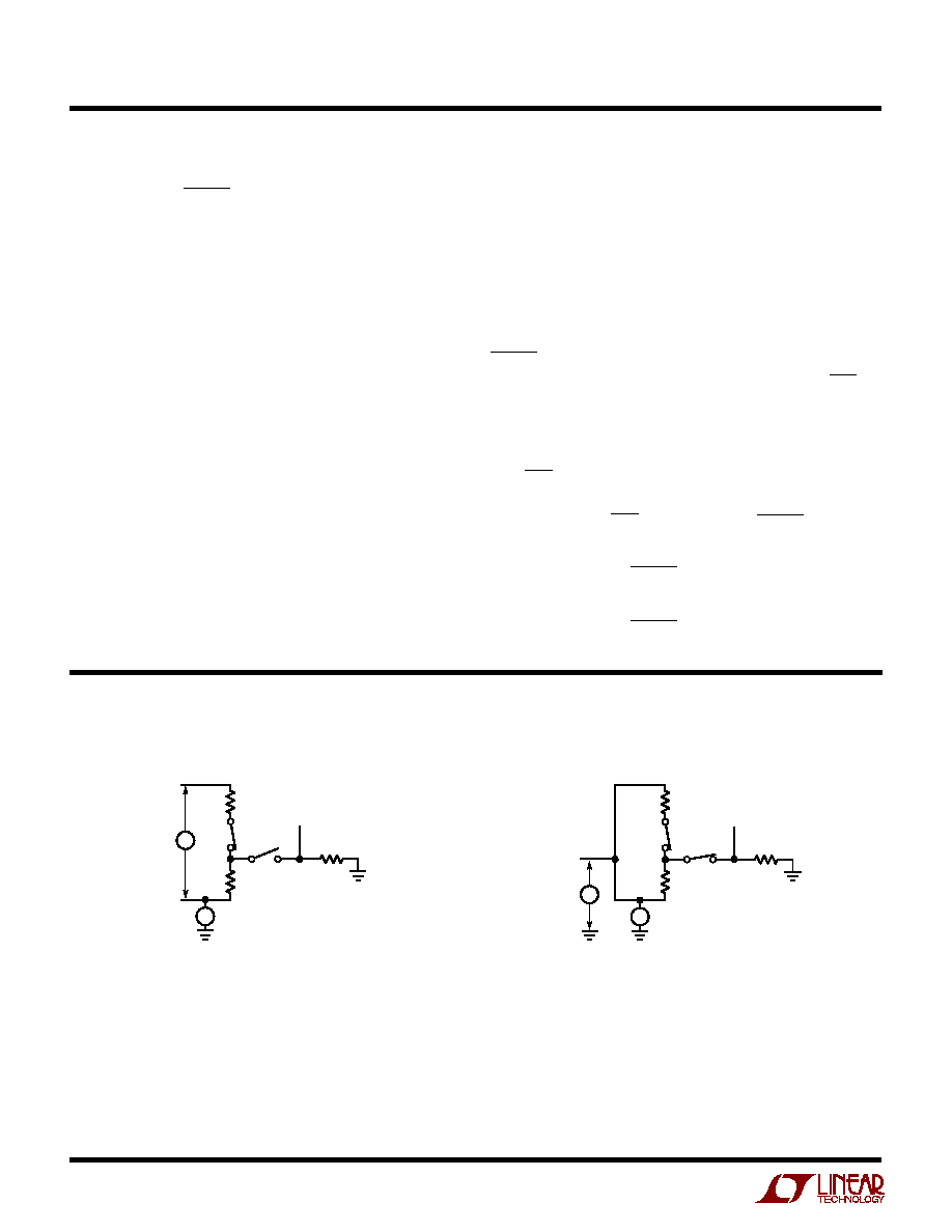
TEST CIRCUITS
PI
N
FU
N
CTIO
N
S
U
U
U
M0 (Pin 1): TTL Level Mode Select Input. The data on M0
is latched when LATCH is high.
V
EE
(Pin 2): Negative Supply Voltage Input. Can connect
directly to the LTC1343 V
EE
pin.
R1C (Pin 3): Load 1 Center Tap.
R1B (Pin 4): Load 1 Node B.
R1A (Pin 5): Load 1 Node A.
R2A (Pin 6): Load 2 Node A.
R2B (Pin 7): Load 2 Node B.
R2C (Pin 8): Load 2 Center Tap.
R3A (Pin 9): Load 3 Node A.
R2B (Pin 10): Load 2 Node B.
R3C (Pin 11): Load 3 Center Tap.
GND (Pin 12): Ground Connection for Load 1 to Load 3.
GND (Pin 13): Ground Connection for Load 4 to Load 6.
V
CC
(Pin 14): Positive Supply Input. 4.75V
V
CC
5.25V.
R4B (Pin 15): Load 4 Node B.
R4A (Pin 16): Load 4 Node A.
R5B (Pin 17): Load 5 Node B.
R5A (Pin 18): Load 5 Node A.
R6A (Pin 19): Load 6 Node A.
R6B (Pin 20): Load 6 Node B.
LATCH (Pin 21): TTL Level Logic Signal Latch Input. When
it is low the input buffers on M0, M1, M2 and DCE/DTE are
transparent. When it is high the logic pins are latched into
their respective input buffers. The data latch allows the
select lines to be shared between multiple I/O ports.
DCE/DTE (Pin 22): TTL Level Mode Select Input. The DCE
mode is selected when it is high and DTE mode when low.
The data on DCE/DTE is latched when LATCH is high.
M2 (Pin 23): TTL Level Mode Select Input 1. The data on
M2 is latched when LATCH is high.
M1 (Pin 24): TTL Level Mode Select Input 2. The data on
M1 is latched when LATCH is high.
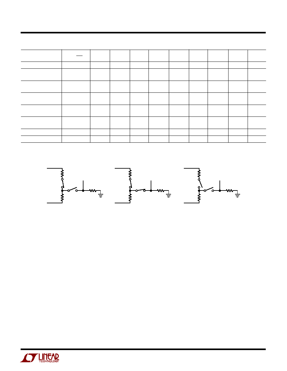
R1
51.5
R2
51.5
±
7V OR
±
2V
1344 F01
R3
124
S2
OFF
S1
ON
C
V
A
B
R1
51.5
R2
51.5
±
2V
1344 F02
R3
124
S2
ON
S1
ON
C
V
A, B
Figure 1. Differential V.11 or V.35 Impedance Measurement
Figure 2. V.35 Common Mode Impedance Measurement
5
LTC1344
LTC1344
MODE NAME
DCE/DTE
M2
M1
M0
R1
R2
R3
R4
R5
R6
V.10/RS423
X
0
0
0
Z
Z
Z
Z
Z
Z
RS530A
0
0
0
1
Z
Z
Z
V.11
V.11
V.11
1
0
0
1
Z
Z
Z
Z
V.11
V.11
Reserved
0
0
1
0
Z
Z
Z
V.11
V.11
V.11
1
0
1
0
V.11
V.11
V.11
Z
Z
Z
X.21
0
0
1
1
Z
Z
Z
V.11
V.11
V.11
1
0
1
1
Z
Z
Z
Z
V.11
V.11
V.35
0
1
0
0
V.35
V.35
Z
V.35
V.35
V.35
1
1
0
0
V.35
V.35
V.35
Z
V.35
V.35
RS530/RS449/V.36
0
1
0
1
Z
Z
Z
V.11
V.11
V.11
1
1
0
1
Z
Z
Z
Z
V.11
V.11
V.28/RS232
X
1
1
0
Z
Z
Z
Z
Z
Z
No Cable
X
1
1
1
V.11
V.11
V.11
V.11
V.11
V.11
X = don't care, 0 = logic low, 1 = logic high
ODE SELECTIO
W U
R1
51.5
R2
51.5
R3
124
S2
OFF
S1
ON
C
V.11 Mode
V.35 Mode
Hi-Z Mode
A
B
R1
51.5
R2
51.5
R3
124
S2
ON
S1
ON
C
A
B
R1
51.5
R2
51.5
1344 F03
R3
124
C
A
B
S2
OFF
S1
OFF
Figure 3. LTC1344 Modes