 | ÐлекÑÑоннÑй компоненÑ: LTC1391C | СкаÑаÑÑ:  PDF PDF  ZIP ZIP |
Äîêóìåíòàöèÿ è îïèñàíèÿ www.docs.chipfind.ru
1
LTC1391
8-Channel
Analog Multiplexer with
Cascadable Serial Interface
s
Low R
ON
: 45
s
Single 2.7V to
±
5V Supply Operation
s
Analog Inputs May Extend to Supply Rails
s
Low Charge Injection
s
Serial Digital Interface
s
Low Leakage:
±
5nA Max
s
Guaranteed Break-Before-Make
s
TTL/CMOS Compatible for All Digital Inputs
s
Cascadable to Allow Additional Channels
s
Can Be Used as a Demultiplexer
FEATURES
DESCRIPTIO
N
U
The LTC
®
1391 is a high performance CMOS 8-to-1 analog
multiplexer. It features a serial digital interface that allows
several LTC1391s to be daisy-chained together, increas-
ing the number of MUX channels available using a single
digital port.
The LTC1391 features a typical R
ON
of 45
, a typical
switch leakage of 50pA and guaranteed break-before-
make operation. Charge injection is
±
10pC maximum. All
digital inputs are TTL and CMOS compatible when oper-
ated from single or dual supplies. The inputs can with-
stand 100mA fault current.
The LTC1391 is available in 16-pin PDIP, SSOP and
narrow SO packages. For applications requiring 2-way
serial data transmission, see the LTC1390 data sheet.
s
Data Acquisition Systems
s
Communication Systems
s
Signal Multiplexing/Demultiplexing
APPLICATIO
N
S
U
, LTC and LT are registered trademarks of Linear Technology Corporation.
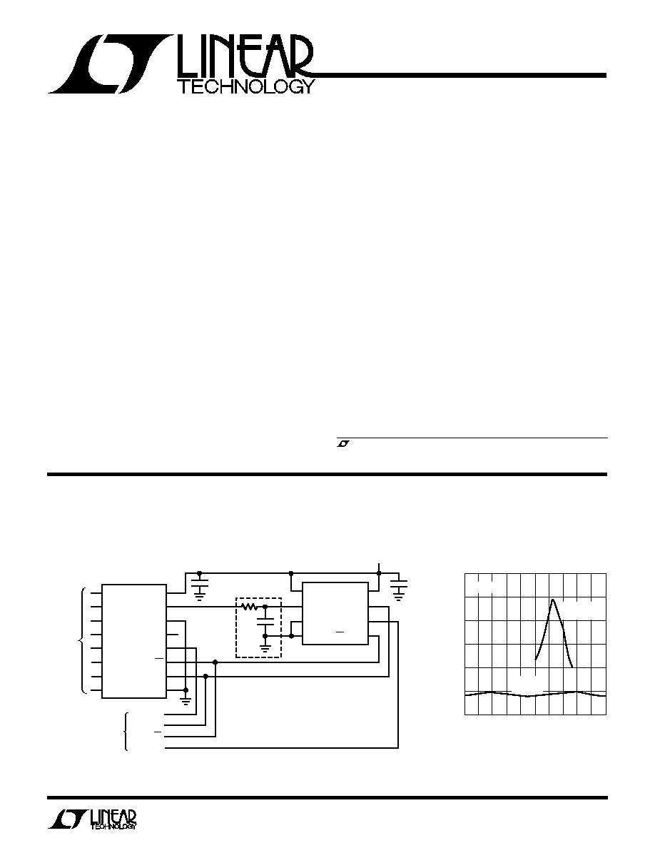
TYPICAL APPLICATIO
N
U
1
2
3
4
5
6
7
8
16
15
14
13
12
11
10
9
S0
S1
S2
S3
S4
S5
S6
S7
V
+
D
V
D
OUT
D
IN
CS
CLK
GND
ANALOG
INPUTS
LTC1391
1
2
3
4
8
7
6
5
V
CC
CLK
D
OUT
CS/SHDN
V
REF
+IN
IN
GND
LTC1285
3V
0.1
µ
F
OPTIONAL A/D
INPUT FILTER
1
µ
F
DATA IN
CLK
CS
DATA OUT
SERIAL INTERFACE
TO MUX AND ADC
1391 TA01
ANALOG INPUT VOLTAGE (V)
5 4
2
0
2
4
ON-RESISTANCE (
)
300
250
200
150
100
50
0
3
1
1
3
1391 TA02
5
T
A
= 25
°
C
V
+
= 2.7V
V
= 0V
V
+
= 5V
V
= 5V
On-Resistance vs
Analog Input Voltage
3V, 8-Channel 12-Bit ADC
2
LTC1391
ABSOLUTE
M
AXI
M
U
M
RATINGS
W
W
W
U
PACKAGE/ORDER I
N
FOR
M
ATIO
N
W
U
U
ORDER PART
NUMBER
LTC1391CGN
LTC1391CN
LTC1391CS
LTC1391IGN
LTC1391IN
LTC1391IS
Consult factory for Military grade parts.
V
+
= 5V, V
= 5V, GND = 0V, T
A
= operating temperature range, unless otherwise specified.
ELECTRICAL CHARACTERISTICS
SYMBOL PARAMETER
CONDITIONS
MIN
TYP
MAX
UNITS
Switch
V
ANALOG
Analog Signal Range
(Note 2)
q
5
5
V
R
ON
On-Resistance
V
S
=
±
3.5V
T
MIN
75
I
D
= 1mA
25
°
C
45
75
T
MAX
120
R
ON
vs V
S
20
%
R
ON
vs Temperature
0.5
%/
°
C
I
S(OFF)
Off Input Leakage
V
S
= 4V, V
D
= 4V, V
S
= 4V, V
D
= 4V
±
0.05
±
5
nA
Channel Off
q
±
20
nA
I
D(OFF)
Off Output Leakage
V
S
= 4V, V
D
= 4V, V
S
= 4V, V
D
= 4V
±
0.05
±
5
nA
Channel Off
q
±
20
nA
I
D(ON)
On Channel Leakage
V
S
= V
D
=
±
4V
±
0.05
±
5
nA
Channel On
q
±
20
nA
Digital
V
INH
High Level Input Voltage
V
+
= 5.25V
q
2.4
V
V
INL
Low Level Input Voltage
V
+
= 4.75V
q
0.8
V
I
INL
, I
INH
Input Current
V
IN
= 5V, 0V
q
±
5
µ
A
V
OH
High Level Output Voltage
V
+
= 4.75V, I
O
= 10
µ
A
4.74
V
I
O
= 360
µ
A
q
2.4
4.50
V
V
OL
Low Level Output Voltage
V
+
= 4.75V, I
O
= 1.6mA
q
0.5
0.8
V
Dynamic
f
CLK
Clock Frequency
(Note 2)
5
MHz
t
ON
Enable Turn-On Time
V
S
= 2.5V, R
L
= 1k, C
L
= 35pF
260
400
ns
t
OFF
Enable Turn-Off Time
V
S
= 2.5V, R
L
= 1k, C
L
= 35pF
100
200
ns
t
OPEN
Break-Before-Make Interval
35
155
ns
OIRR
Off Isolation
V
S
= 2V
PP
, R
L
= 1k, f = 100kHz
70
dB
Q
INJ
Charge Injection
R
S
= 0, C
L
= 1000pF, V
S
= 1V (Note 2)
±
2
±
10
pC
Total Supply Voltage (V
+
to V
) .............................. 15V
Input Voltage
Analog Inputs ................... (V
0.3V) to (V
+
+ 0.3V)
Digital Inputs ......................................... 0.3V to 15V
Digital Outputs .......................... 0.3V to (V
+
+ 0.3V)
Power Dissipation .............................................. 500mW
Operating Temperature Range
LTC1391C ............................................... 0
°
C to 70
°
C
LTC1391I ........................................... 40
°
C to 85
°
C
Storage Temperature Range ................. 65
°
C to 150
°
C
Lead Temperature (Soldering, 10 sec).................. 300
°
C
T
JMAX
= 125
°
C,
JA
= 110
°
C/ W (GN)
T
JMAX
= 125
°
C,
JA
= 70
°
C/ W (N)
T
JMAX
= 125
°
C,
JA
= 100
°
C/ W (S)
(Note 1)
1
2
3
4
5
6
7
8
TOP VIEW
N PACKAGE
16-LEAD PDIP
GN PACKAGE
16-LEAD PLASTIC SSOP
S PACKAGE
16-LEAD PLASTIC SO
16
15
14
13
12
11
10
9
S0
S1
S2
S3
S4
S5
S6
S7
V
+
D
V
D
OUT
D
IN
CS
CLK
GND
GN PART MARKING
1391
1391I
3
LTC1391
V
+
= 5V, V
= 5V, GND = 0V, T
A
= operating temperature range, unless otherwise specified.
SYMBOL PARAMETER
CONDITIONS
MIN
TYP
MAX
UNITS
Dynamic
C
S(OFF)
Input Off Capacitance
5
pF
C
D(0FF)
Output Off Capacitance
10
pF
Supply
I
+
Positive Supply Current
All Logic Inputs Tied Together, V
IN
= 0V or 5V
q
15
40
µ
A
I
Negative Supply Current
All Logic Inputs Tied Together, V
IN
= 0V or 5V
q
15
40
µ
A
V
+
= 2.7V, V
= GND = 0V, T
A
= operating temperature range, unless otherwise specified.
SYMBOL PARAMETER
CONDITIONS
MIN
TYP
MAX
UNITS
Switch
V
ANALOG
Analog Signal Range
(Note 2)
q
0
2.7
V
R
ON
On-Resistance
V
S
= 1.2V
T
MIN
300
I
O
= 1mA
25
°
C
250
300
T
MAX
350
R
ON
vs V
S
20
%
R
ON
vs Temperature
0.5
%/
°
C
I
S(OFF)
Off Input Leakage
V
S
= 2.5V, V
D
= 0.5V; V
S
= 0.5V, V
D
= 2.5V (Note 3)
±
0.05
±
5
nA
Channel Off
q
±
20
nA
I
D(OFF)
Off Output Leakage
V
S
= 2.5V, V
D
= 0.5V; V
S
= 0.5V, V
D
= 2.5V (Note 3)
±
0.05
±
5
nA
Channel Off
q
±
20
nA
I
D(ON)
On Channel Leakage
V
S
= V
D
= 0.5V, 2.5V (Note 3)
±
0.05
±
5
nA
Channel On
q
±
20
nA
Digital
V
INH
High Level Input Voltage
V
+
= 3.0V
q
2.0
V
V
INL
Low Level Input Voltage
V
+
= 2.4V
q
0.8
V
I
INL
, I
INH
Input Current
V
IN
= 2.7V, 0V
q
±
5
µ
A
V
OH
High Level Output Voltage
V
+
= 2.7V, I
O
= 20
µ
A
2.68
V
I
O
= 400
µ
A
q
2.0
2.30
V
V
OL
Low Level Output Voltage
V
+
= 2.7V, I
O
= 20
µ
A
0.01
V
I
O
= 400
µ
A
q
0.20
0.8
V
Dynamic
f
CLK
Clock Frequency
(Note 2)
5
MHz
t
ON
Enable Turn-On Time
V
S
= 1.5V, R
L
= 1k, C
L
= 35pF (Note 4)
490
800
ns
t
OFF
Enable Turn-Off Time
V
S
= 1.5V, R
L
= 1k, C
L
= 35pF (Note 4)
190
400
ns
t
OPEN
Break-Before-Make Interval
(Note 4)
125
290
ns
QIRR
Off Isolation
V
S
= 2V
PP
, R
L
= 1k, f = 100kHz
70
dB
Q
INJ
Charge Injection
R
S
= 0, C
L
= 1000pF, V
S
= 1V (Note 2)
±
1
±
5
pC
C
S(OFF)
Input Off Capacitance
5
pF
C
D(OFF)
Output Off Capacitance
10
pF
Supply
I
+
Positive Supply Current
All Logic Inputs Tied Together, V
IN
= 0V or 2.7V
q
0.2
2
µ
A
The
q
denotes specifications which apply over the full operating
temperature range.
Note 1: Absolute Maximum Ratings are those values beyond which the life
of a device may be impaired.
Note 2: Guaranteed by Design.
Note 3: Leakage current with a single 2.7V supply is guaranteed by
correlation with the
±
5V leakage current specifications.
Note 4: Timing specifications with a single 2.7V supply are guaranteed by
correlation with the
±
5V timing specifications.
ELECTRICAL CHARACTERISTICS
4
LTC1391
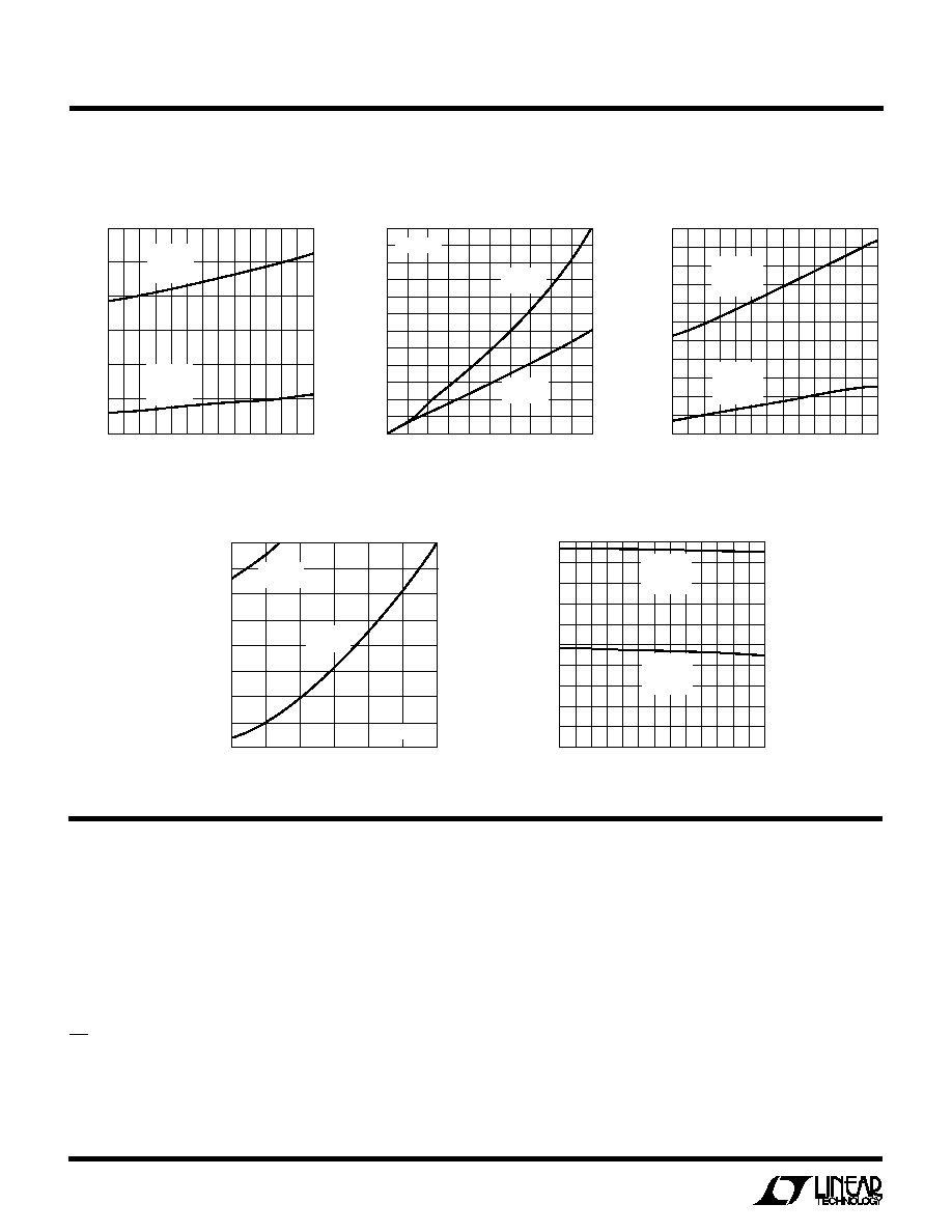
TYPICAL PERFOR
M
A
N
CE CHARACTERISTICS
U
W
TEMPERATURE (
°
C)
40
20
ON-RESISTANCE (
)
300
250
200
150
100
50
0
80
1391 G01
0
20
40
60
V
+
= 2.7V
V
= 0V
V
S
= 1.2V
V
+
= 5V
V
= 5V
V
S
= 0V
On-Resistance vs Temperature
TEMPERATURE (
°
C)
40
OUTPUT VOLTAGE (V)
0.65
0.60
0.55
0.50
0.45
0.40
0.35
0.30
0.25
0.20
0.15
0.10
60
1391 G03
20
0
20
40
80
V
+
= 5V
V
= 5V
I
O
= 1.8mA
V
+
= 2.7V
V
= 0V
I
O
= 400
µ
A
OUTPUT CURRENT (mA)
0
OUTPUT VOLTAGE (V)
0.4
0.8 1.0
2.0
1.8
1391 G02
0.2
0.6
1.2 1.4 1.6
1.2
1.1
1.0
0.9
0.8
0.7
0.6
0.5
0.4
0.3
0.2
0.1
0
T
A
= 25
°
C
V
+
= 2.7V
V
= 0V
V
+
= 5V
V
= 5V
Driver Output Low Voltage
vs Output Current
Driver Output Low Voltage
vs Temperature
OUTPUT VOLTAGE (V)
2.0
2.5
OUTPUT CURRENT (mA)
3.0
4.0
3.5
4.5
5.0
1391 G04
0
0.5
1.0
1.5
2.0
2.5
3.0
3.5
4.0
V
+
= 5V
V
= 5V
T
A
=25
°
C
V
+
= 2.7V
V
= 0V
TEMPERATURE (
°
C)
40
OUTPUT VOLTAGE (V)
5.0
4.5
4.0
3.5
3.0
2.5
2.0
1.5
1.0
0.5
0
60
1391 G05
20
0
20
40
80
V
+
= 5V
V
= 5V
I
O
= 1.6mA
V
+
= 2.7V
V
= 0V
I
O
= 400
µ
A
PI
N
FU
N
CTIO
N
S
U
U
U
S0, S1, S2, S3, S4, S5, S6, S7 (Pins 1, 2, 3, 4, 5, 6, 7,
8): Analog Multiplexer Inputs.
GND (Pin 9): Digital Ground. Connect to system ground.
CLK (Pin 10): System Clock (TTL/CMOS Compatible). The
clock synchronizes the channel selection bits and the
serial data transfer from D
IN
to D
OUT
.
CS (Pin 11): Channel Select Input (TTL/CMOS Compat-
ible). A logic high on this input enables the LTC1391 to
read in the channel selection bits and allows digital data
transfer from D
IN
to D
OUT
. A logic low on this input puts
D
OUT
into three-state and enables the selected channel for
analog signal transmission.
D
IN
(Pin 12): Digital Input (TTL/CMOS Compatible). Input
for the channel selection bits.
D
OUT
(Pin 13): Digital Output (TTL/CMOS Compatible).
Output from the internal shift register.
V
(Pin 14): Negative Supply.
D (Pin 15): Analog Multiplexer Output.
V
+
(Pin 16): Positive Supply.
Driver Output High Voltage
vs Output Current
Driver Output High Voltage
vs Temperature
5
LTC1391
APPLICATIO
N
S I
N
FOR
M
ATIO
N
W
U
U
U
Multiplexer Operation
Figure 1 shows the block diagram of the components
within the LTC1391 required for MUX operation. The
LTC1391 uses D
IN
to select the active channel and the chip
select input, CS, to switch on the selected channel as
shown in Figure 2.
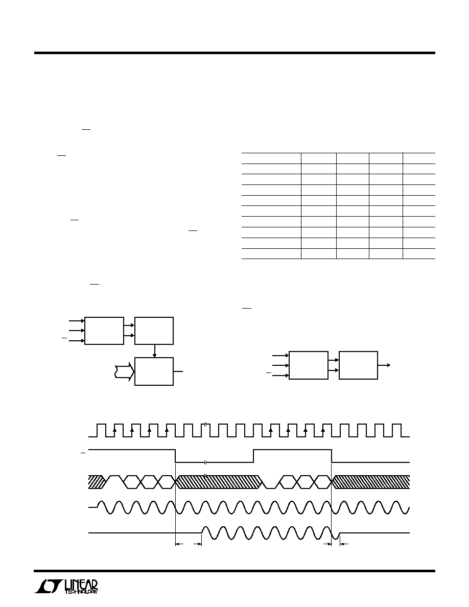
When CS is high, the input data on the D
IN
pin is latched
into the 4-bit shift register on the rising clock edge. The
input data consists of the "EN" bit and a string of three bits
for channel selection. If "EN" bit is logic high as illustrated
in the first input data sequence, it enables the selected
channel. After the clocking in of the last channel selection
bit B0, the CS pin must be pulled low before the next rising
clock edge to ensure correct operation. Once CS is pulled
low, the previously selected channel is switched off to
ensure a break-before-make interval. After a delay of t
ON
,
the selected channel is switched on allowing signal trans-
mission. The selected channel remains on until the next
falling edge of CS. After a delay of t
OFF
, the LTC1391
terminates the analog signal transmission and allows the
selection of next channel. If the "EN" bit is logic low, as
illustrated in the second data sequence, it disables all
channels and there will be no analog signal transmission.
Table 1 shows the various bit combinations for channel
selection.
Table 1. Logic Table for Channel Selection
ACTIVE CHANNEL
EN
B2
B1
BO
All Off
0
X
X
X
S0
1
0
0
0
S1
1
0
0
1
S2
1
0
1
0
S3
1
0
1
1
S4
1
1
0
0
S5
1
1
0
1
S6
1
1
1
0
S7
1
1
1
1
Digital Data Transfer Operation
The block diagram of Figure 3 shows the components
within the LTC1391 required for serial data transfer. When
CS is held high, data is fed into the 4-bit shift register and
then shifted to D
OUT
. Data appears at D
OUT
after the fourth
rising edge of the clock as shown in Figure 4. The last four
Figure 2. Multiplexer Operation
EN
HIGH
B2
EN LO
B2
B1
B0
B1
B0
CLK
CS
D
IN
ANY ANALOG
INPUT
D
t
ON
t
OFF
1391 · F02
Figure 1. Simplified Block Diagram of the MUX Operation
CONTROL
LOGIC
4-BIT SHIFT
REGISTER
MUX
BLOCK
CLK
D
IN
CS
1391 · F01
ANALOG
OUTPUT (D)
ANALOG INPUTS
(S0 TO S7)
Figure 3. Simplified Block Diagram of the
Digital Data Transfer Operation
CONTROL
LOGIC
4-BIT SHIFT
REGISTER
CLK
D
IN
CS
1391 F03
D
OUT