 | –≠–ª–µ–∫—Ç—Ä–æ–Ω–Ω—ã–π –∫–æ–º–ø–æ–Ω–µ–Ω—Ç: LTC1417I | –°–∫–∞—á–∞—Ç—å:  PDF PDF  ZIP ZIP |
1
LTC1417
Low Power 14-Bit, 400ksps
Sampling ADC Converter
with Serial I/O
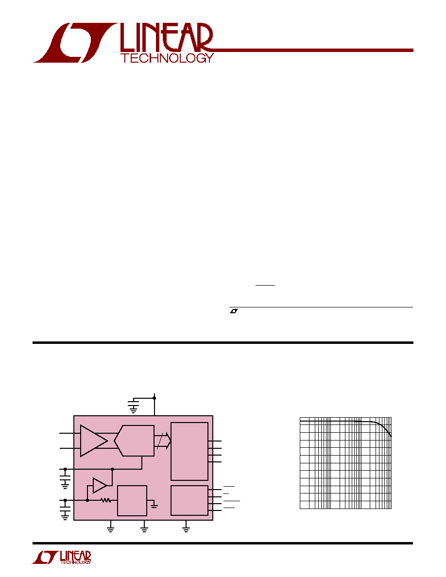
A 400kHz, 14-Bit Sampling A/D Converter in a Narrow 16-Lead SSOP Package
Effective Bits and Signal-to-(Noise + Distortion)
vs Input Frequency
The LTC
Æ
1417 is a low power, 400ksps, 14-bit A/D con-
verter. This versatile device can operate from a single 5V or
±
5V supplies. An onboard high performance sample-and-
hold, a precision reference and internal trimming minimize
external circuitry requirements. The low 20mW power
dissipation is made even more attractive with two user-
selectable power shutdown modes.
The LTC1417 converts 0V to 4.096V unipolar inputs when
using a 5V supply and
±
2.048V bipolar inputs when using
±
5V supplies. DC specs include
±
1.25LSB INL,
±
1LSB
DNL and no missing codes over temperature. Outstanding
AC performance includes 81dB S/(N + D) and 95dB THD
at a Nyquist input frequency of 200kHz.
The internal clock is trimmed for 2
µ
s maximum conver-
sion time. A separate convert start input and a data ready
signal (BUSY) ease connections to FIFOs, DSPs and
microprocessors.
s
16-Pin Narrow SSOP Package (SO-8 Footprint)
s
Sample Rate: 400ksps
s
±
1.25LSB INL and
±
1LSB DNL Max
s
Power Dissipation: 20mW (Typ)
s
Single Supply 5V or
±
5V Operation
s
Serial Data Output
s
No Missing Codes Over Temperature
s
Power Shutdown: Nap and Sleep
s
External or Internal Reference
s
Differential High Impedance Analog Input
s
Input Range: 0V to 4.096V or
±
2.048V
s
81dB S/(N + D) and ≠ 95dB THD at Nyquist
s
High Speed Data Acquisition
s
Digital Signal Processing
s
Isolated Data Acquisition Systems
s
Audio and Telecom Processing
s
Spectrum Instrumentation
, LTC and LT are registered trademarks of Linear Technology Corporation.
FEATURES
DESCRIPTIO
U
APPLICATIO S
U
S/H
14
BUFFER
8k
10
µ
F
10
µ
F
REFCOMP
A
IN
≠
A
IN
+
V
REF
4.096V
5V
LTC1417
14-BIT ADC
SERIAL
PORT
DGND
10
15
5
3
4
2
1
1417 TA01
V
SS
(0V OR ≠ 5V)
AGND
EXTCLKIN
SCLK
CLKOUT
D
OUT
V
DD
16
TIMING AND
LOGIC
2.5V
REFERENCE
BUSY
RD
CONVST
SHDN
1
µ
F
6
7
8
9
14
12
13
11
INPUT FREQUENCY (Hz)
4
EFFECTIVE BITS
S/(N + D) (dB)
6
8
10
12
10k
100k
1M
1417 TA02
2
1k
14
86
80
74
68
62
EQUIVALE T BLOCK DIAGRA
W
U
2
LTC1417
(Notes 1, 2)
Positive Supply Voltage (V
DD
) .................................. 6V
Negative Supply Voltage (V
SS
)
Bipolar Operation Only .......................... ≠ 6V to GND
Total Supply Voltage (V
DD
to V
SS
)
Bipolar Operation Only ....................................... 12V
Analog Input Voltage (Note 3)
Unipolar Operation .................. ≠ 0.3V to (V
DD
+ 0.3V)
Bipolar Operation............ (V
SS
≠ 0.3) to (V
DD
+ 0.3V)
Digital Input Voltage (Note 4)
Unipolar Operation ............................... ≠ 0.3V to 10V
Bipolar Operation.........................(V
SS
≠ 0.3V) to 10V
Digital Output Voltage
Unipolar Operation ................... ≠ 0.3 to (V
DD
+ 0.3V)
Bipolar Operation........... (V
SS
≠ 0.3V) to (V
DD
+ 0.3V)
Power Dissipation ............................................. 500mW
Operating Temperature Range
LTC1417C .............................................. 0
∞
C to 70
∞
C
LTC1417I ............................................ ≠ 40
∞
C to 85
∞
C
Storage Temperature Range ................ ≠ 65
∞
C to 150
∞
C
Lead Temperature (Soldering, 10 sec)................. 300
∞
C
A
U
G
W
A
W
U
W
A
R
BSOLUTE
XI
TI
S
W
U
U
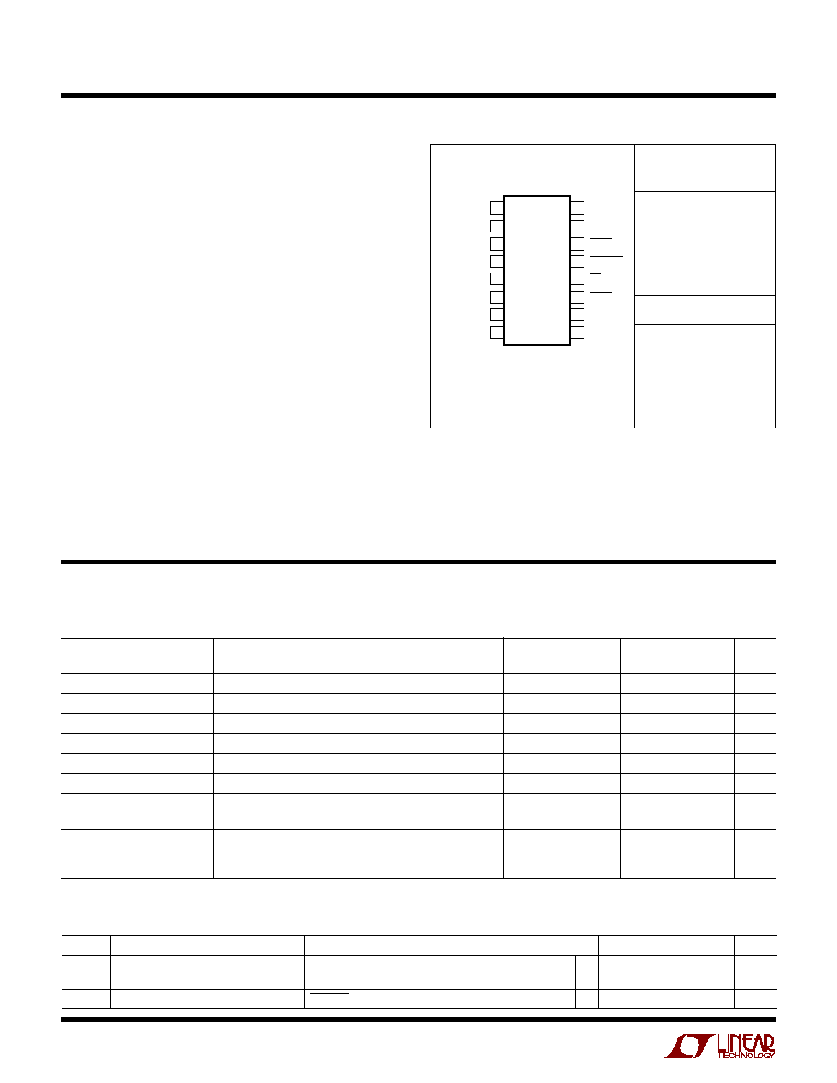
PACKAGE/ORDER I FOR ATIO
ORDER
PART NUMBER
T
JMAX
= 110
∞
C,
JA
= 95
∞
C/W
LTC1417
LTC1417A
PARAMETER
CONDITIONS
MIN
TYP
MAX
MIN
TYP
MAX
UNITS
Resolution
q
14
14
Bits
No Missing Codes
q
13
14
Bits
Integral Linearity Error
(Note 7)
q
±
0.8
±
2
±
0.5
±
1.25
LSB
Differential Linearity Error
q
±
0.7
±
1.5
±
0.35
±
1
LSB
Transition Noise
(Note 12)
0.33
0.33
LSB
RMS
Offset Error
External Reference (Note 8)
q
±
5
±
20
±
2
±
10
LSB
Full-Scale Error
Internal Reference
±
15
±
60
±
15
±
60
LSB
External Reference = 2.5V
±
5
±
30
±
5
±
15
LSB
Full-Scale Tempco
I
OUT(REF)
= 0, Internal Reference, 0
∞
C
T
A
70
∞
C
±
15
±
10
ppm/
∞
C
I
OUT(REF)
= 0, Internal Reference, ≠ 40
∞
C
T
A
85
∞
C
±
20
ppm/
∞
C
I
OUT(REF)
= 0, External Reference
±
5
±
1
ppm/
∞
C
C
C
HARA TERISTICS
CO
U
VERTER
LTC1417ACGN
LTC1417CGN
LTC1417AIGN
LTC1417IGN
GN PART MARKING
Consult factory for Military grade parts.
1417A
1417
1417AI
1417I
GN PACKAGE
16-LEAD (NARROW) PLASTIC SSOP
1
2
3
4
5
6
7
8
TOP VIEW
16
15
14
13
12
11
10
9
A
IN
+
A
IN
≠
V
REF
REFCOMP
AGND
EXTCLKIN
SCLK
CLKOUT
V
DD
V
SS
BUSY
CONVST
RD
SHDN
DGND
D
OUT
The
q
indicates specifications which apply over the full operating
temperature range, otherwise specifications are at T
A
= 25
∞
C. Specifications are measured while using the internal reference unless
otherwise noted. (Notes 5, 6)
SYMBOL
PARAMETER
CONDITIONS
MIN
TYP
MAX
UNITS
V
IN
Analog Input Range (Note 9)
4.75V
V
DD
5.25V (Unipolar)
q
0 to 4.096
V
4.75V
V
DD
5.25V, ≠ 5.25V
V
SS
≠ 4.75V (Bipolar)
q
±
2.048
V
I
IN
Analog Input Leakage Current
CONVST = High
q
±
1
µ
A
The
q
indicates specifications which apply over the full operating temperature range,
otherwise specifications are at T
A
= 25
∞
C. (Note 5)
A ALOG I PUT
U
U
3
LTC1417
SYMBOL
PARAMETER
CONDITIONS
MIN
TYP
MAX
UNITS
C
IN
Analog Input Capacitance
Between Conversions (Sample Mode)
14
pF
During Conversions (Hold Mode)
3
pF
t
ACQ
Sample-and-Hold Acquisition Time
q
150
500
ns
t
AP
Sample-and-Hold Aperture Time
≠1.5
ns
t
jitter
Sample-and-Hold Aperture Time Jitter
5
ps
RMS
CMRR
Analog Input Common Mode Rejection Ratio
0V < (A
IN
+
= A
IN
≠
) < 4.096V (Unipolar)
65
dB
≠ 2.048V < (A
IN
+
= A
IN
≠
) < 2.048V (Bipolar)
65
dB
SYMBOL
PARAMETER
CONDITIONS
MIN
TYP
MAX
UNITS
S/(N + D)
Signal-to-(Noise + Distortion) Ratio
100kHz Input Signal
q
79
81
dB
THD
Total Harmonic Distortion
100kHz Input Signal, First Five Harmonics
q
≠ 85
≠ 95
dB
SFDR
Spurious Free Dynamic Range
200kHz Input Signal
≠ 98
dB
IMD
Intermodulation Distortion
f
IN1
= 97.3kHz, f
IN2
= 104.6kHz
≠ 97
dB
Full Power Bandwidth
10
MHz
Full Linear Bandwidth
S/(N + D)
77dB
0.8
MHz
PARAMETER
CONDITIONS
MIN
TYP
MAX
UNITS
V
REF
Output Voltage
I
OUT
= 0
q
2.480
2.500
2.520
V
V
REF
Output Tempco
I
OUT
= 0, 0
∞
C
T
A
70
∞
C
±
10
ppm/
∞
C
I
OUT
= 0, ≠ 40
∞
C
T
A
85
∞
C
±
20
ppm/
∞
C
V
REF
Line Regulation
4.75V
V
DD
5.25V
0.05
LSB/V
≠ 5.25V
V
SS
≠ 4.75V
0.05
LSB/V
V
REF
Output Resistance
0.1mA
|
I
OUT
|
0.1mA
8
k
SYMBOL
PARAMETER
CONDITIONS
MIN
TYP
MAX
UNITS
V
IH
High Level Input Voltage
V
DD
= 5.25V
q
2.4
V
V
IL
Low Level Input Voltage
V
DD
= 4.75V
q
0.8
V
I
IN
Digital Input Current
V
IN
= 0V to V
DD
q
±
10
µ
A
C
IN
Digital Input Capacitance
1.4
pF
V
OH
High Level Output Voltage
V
DD
= 4.75V, I
O
= ≠ 10
µ
A
4.74
V
V
DD
= 4.75V, I
O
= ≠ 200
µ
A
q
4.0
V
V
OL
Low Level Output Voltage
V
DD
= 4.75V, I
O
= 160
µ
A
0.05
V
V
DD
= 4.75V, I
O
= ≠ 1.6mA
q
0.10
0.4
V
I
OZ
High-Z Output Leakage D
OUT
, CLKOUT
V
OUT
= 0V to V
DD
, RD High
q
±
10
µ
A
C
OZ
High-Z Output Capacitance D
OUT
, CLKOUT
RD High (Note 9)
q
15
pF
I
SOURCE
Output Source Current
V
OUT
= 0V
≠ 10
mA
I
SINK
Output Sink Current
V
OUT
= V
DD
10
mA
The
q
indicates specifications which apply over the full operating temperature range,
otherwise specifications are at T
A
= 25
∞
C. (Note 5)
A ALOG I PUT
U
U
The
q
indicates specifications which apply over the full operating temperature range,
otherwise specifications are at T
A
= 25
∞
C. (Note 5)
DY
A
IC ACCURACY
U
W
I TER AL REFERE CE CHARACTERISTICS
U
U
U
DIGITAL I PUTS A D DIGITAL OUTPUTS
U
U
The
q
indicates specifications which apply over the full
operating temperature range, otherwise specifications are at T
A
= 25
∞
C. (Note 5)
The
q
indicates specifications which apply over the full
operating temperature range, otherwise specifications are at T
A
= 25
∞
C. (Note 5)
4
LTC1417
SYMBOL
PARAMETER
CONDITIONS
MIN
TYP
MAX
UNITS
f
SAMPLE(MAX)
Maximum Sampling Frequency
q
400
kHz
t
CONV
Conversion Time
q
1.8
2.25
µ
s
t
ACQ
Acquisition Time
q
150
500
ns
t
ACQ
+ t
CONV
Acquisition Plus Conversion Time
q
2.1
2.5
µ
s
t
1
SHDN
to CONVST
Wake-Up Time from Nap Mode
(Note 10)
500
ns
t
2
CONVST
Low Time
(Notes 10, 11)
q
40
ns
t
3
CONVST to BUSY Delay
C
L
= 25pF
q
35
70
ns
t
4
Data Ready Before BUSY
C
L
= 25pF
q
7
12
ns
t
5
Delay Between Conversions
(Note 10)
q
250
ns
t
6
Wait Time RD
After BUSY
q
≠ 5
ns
t
7
Data Access Time After RD
C
L
= 25pF
15
30
ns
q
40
ns
C
L
= 100pF
20
40
ns
q
55
ns
t
8
Bus Relinquish Time
q
35
ns
t
9
RD Low Time
q
t
7
ns
t
10
CONVST High Time
q
40
ns
t
11
Delay Time, SCLK
to D
OUT
Valid
C
L
= 25pF
q
15
40
ns
t
12
Time from Previous Data Remain Valid After SCLK
C
L
= 25pF
q
5
10
ns
f
SCLK
Shift Clock Frequency
(Note 13)
q
0
20
MHz
f
EXTCLKIN
External Conversion Clock Frequency
q
0.05
9
MHz
t
dEXTCLKIN
Delay Time, CONVST
to External Conversion Clock Input (Note 9)
q
20
µ
s
SYMBOL
PARAMETER
CONDITIONS
MIN
TYP
MAX
UNITS
V
DD
Positive Supply Voltage (Notes 10, 11)
4.75
5.25
V
V
SS
Negative Supply Voltage (Note 10)
Bipolar Only (V
SS
= 0V for Unipolar)
≠ 4.75
≠ 5.25
V
I
DD
Positive Supply Current
Unipolar, RD High (Note 5)
q
4.0
5.5
mA
Bipolar, RD High (Note 5)
q
4.3
6.0
mA
Nap Mode
SHDN = 0V, RD = 0V
750
µ
A
Sleep Mode
SHDN = 0V, RD = 5V
0.1
µ
A
I
SS
Negative Supply Current
Bipolar, RD High (Note 5)
q
2.0
2.8
mA
Nap Mode
SHDN = 0V, RD = 0V
0.7
µ
A
Sleep Mode
SHDN = 0V, RD = 5V
1.5
nA
P
DIS
Power Dissipation
Unipolar
q
20.0
27.5
mW
Bipolar
q
31.5
44
mW
POWER REQUIRE E TS
W
U
The
q
indicates specifications which apply over the full operating temperature range,
otherwise specifications are at T
A
= 25
∞
C. (Note 5)
The
q
indicates specifications which apply over the full operating temperature
range, otherwise specifications are at T
A
= 25
∞
C. (Note 5)
TI I G CHARACTERISTICS
U
W
5
LTC1417
SYMBOL
PARAMETER
CONDITIONS
MIN
TYP
MAX
UNITS
t
H SCLK
SCLK High Time
(Note 9)
q
10
ns
t
L SCLK
SCLK Low Time
(Note 9)
q
10
ns
t
H EXTCLKIN
EXTCLKIN High Time
q
0.04
20
µ
s
t
L EXTCLKIN
EXTCLKIN Low Time
q
0.04
20
µ
s
Note 1: Absolute Maximum Ratings are those values beyond which the life
of a device may be impaired.
Note 2: All voltage values are with respect to ground with DGND and
AGND wired together (unless otherwise noted).
Note 3: When these pin voltages are taken below V
SS
or above V
DD
, they
will be clamped by internal diodes. This product can handle input currents
greater than 100mA without latchup if the pin is driven below V
SS
(ground
for unipolar mode) or above V
DD
.
Note 4: When these pin voltages are taken below V
SS
they will be clamped
by internal diodes. This product can handle input currents greater than
100mA below V
SS
without latchup. These pins are not clamped to V
DD
.
Note 5: V
DD
= 5V, V
SS
= ≠ 5V, f
SAMPLE
= 400kHz, t
r
= t
f
= 5ns unless
otherwise specified.
Note 6: Linearity, offset and full-scale specifications apply for a single-
ended A
IN
+
input with A
IN
≠
grounded.
Note 7: Integral nonlinearity is defined as the deviation of a code from a
straight line passing through the actual endpoints of the transfer curve.
The deviation is measured from the center of the quantization band.
Note 8: Bipolar offset is the offset voltage measured from ≠ 0.5LSB
when the output code flickers between 0000 0000 0000 00 and
1111 1111 1111 11.
Note 9: Guaranteed by design, not subject to test.
Note 10: Recommended operating conditions.
Note 11: The falling CONVST edge starts a conversion. If CONVST returns
high at a critical point during the conversion it can create small errors. For
best results ensure that CONVST returns high either within 625ns after
conversion start or after BUSY rises.
Note 12: Typical RMS noise at the code transitions. See Figure 2 for
histogram.
Note 13: t
11
of 40ns maximum allows f
SCLK
up to 10MHz for rising
capture with 50% duty cycle. f
SCLK
up to 20MHz for falling capture with
5ns setup time.
TI I G CHARACTERISTICS
U
W
The
q
indicates specifications which apply over the full operating temperature
range, otherwise specifications are at T
A
= 25
∞
C. (Note 5)
TYPICAL PERFOR A CE CHARACTERISTICS
U
W
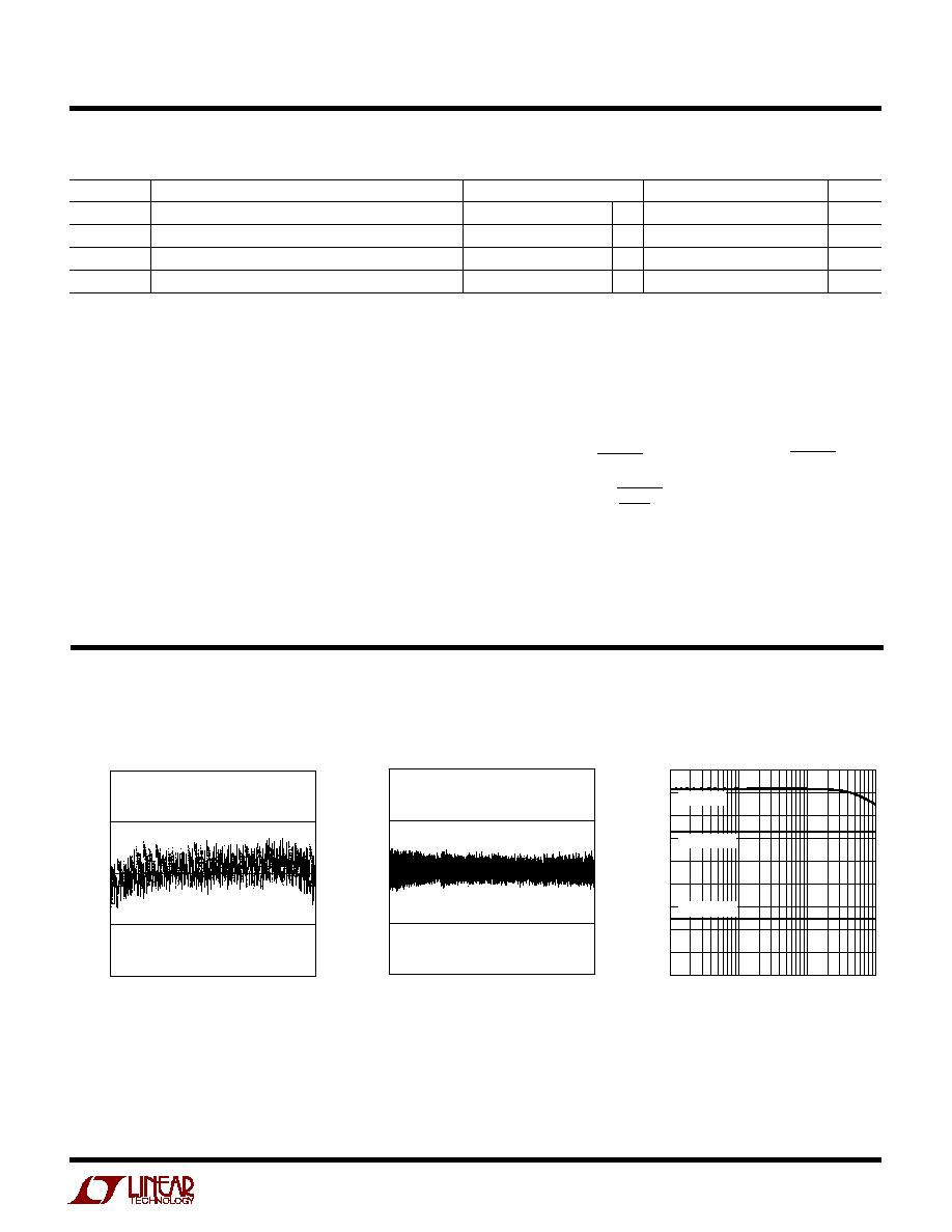
Typical INL Curve
Differential Nonlinearity
vs Output Code
S/(N + D) vs Input Frequency
and Amplitude
OUTPUT CODE
4096
0
≠1.0
INL (LSBs)
≠0.5
0
0.5
1.0
8192
1417 G01
12288
16384
OUTPUT CODE
0
≠1.0
DNL ERROR (LSBs)
≠ 0.5
0
0.5
1.0
4096
8192
1417 G02
12288
16384
(T
A
= 25
∞
C)
INPUT FREQUENCY (Hz)
SIGNAL/(NOISE + DISTORTION) (dB)
90
80
70
60
50
40
30
20
10
0
1k
100k
1M
1417 G03
10k
V
IN
= ≠60dB
V
IN
= 0dB
V
IN
= ≠20dB