14588lfa.pm6 copy

1
LTC1458/LTC1458L
Quad 12-Bit Rail-to-Rail
Micropower DACs
Daisy-Chained Control Outputs
The LTC
®
1458/LTC1458L are complete single supply,
quad rail-to-rail voltage output, 12-bit digital-to-analog
converters (DACs) in SO-28 and SSOP-28 packages. They
include an output buffer amplifier with variable gain (
×
1 or
×
2) and an easy-to-use 3-wire cascadable serial interface.
The LTC1458 has an onboard reference of 2.048V and a
full-scale output of 4.095V in a
×
2 gain configuration. It
operates from a single 4.5V to 5.5V supply dissipating
only 5.5mW (I
CC
= 1.1mA typ).
The LTC1458L has an onboard 1.22V reference and a full-
scale output of 2.5V in a
×
2 gain configuration. It operates
from a single supply of 2.7V to 5.5V dissipating 2.4mW.
Excellent DNL, low supply current and a wide range of
built-in functions allow these parts to be used in a host of
applications when flexibility, power and single supply
operation are important.
s
Quad 12-Bit DAC
s
Buffered True Rail-to-Rail Voltage Output
s
Maximum DNL Error: 0.5LSB
s
5V Operation, I
CC
: 1.1mA Typ (LTC1458)
s
3V Operation, I
CC
: 800
µ
A Typ (LTC1458L)
s
Internal or External Reference Operation
s
Settling Time: 14
µ
s to
±
0.5LSB
s
Schmitt Trigger On Clock Input Allows Direct
Optocoupler Interface
s
Power-On Reset and CLR Pin
s
SSOP-28 Package
s
3-Wire Cascadable Serial Interface with 250kHz
Update Rate
s
Low Cost
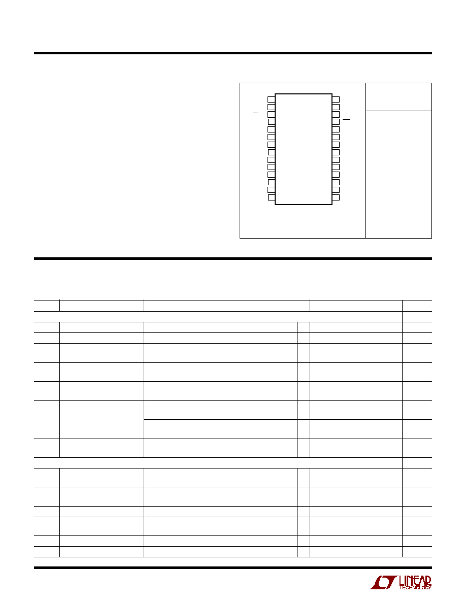
Functional Block Diagram: Quad 12-Bit Rail-to-Rail DAC
Differential Nonlinearity
vs Input Code
s
Digital Calibration
s
Industrial Process Control
s
Automatic Test Equipment
s
Low Power Systems
1458 BD01
48-BIT
SHIFT REGISTER
AND
DAC REGISTER
CLK
D
IN
5V (LTC1458)
3V TO 5V (LTC1458L)
2.048V (LTC1458)
1.22V (LTC1458L)
REFHI C
REFOUT
V
OUT C
V
CC
REFLO C
X1/X2 C
X1/X2 D
X1/X2 A
X1/X2 B
REFHI D
V
OUT D
REFLO D
REFHI B
FROM
µ
P
V
OUT B
REFLO B
REFHI A
V
OUT A
REFLO A
D
OUT
CS/LD
CLR
DAC D
DAC C
DAC B
DAC A
CODE
0
DNL (LSB)
0.5
0.4
0.3
0.2
0.1
0
0.1
0.2
0.3
0.4
0.5
1024
2048 2560
1458 G09
512
1536
3072 3584 4095
DESCRIPTIO
U
FEATURES
APPLICATIO S
U
TYPICAL APPLICATIO
U
, LTC and LT are registered trademarks of Linear Technology Corporation.
2
LTC1458/LTC1458L
(Note 1)
V
CC
to GND .............................................. 0.5V to 7.5V
Logic Inputs to GND ................................ 0.5V to 7.5V
V
OUT A
, V
OUT B
, V
OUT C
, V
OUT D
,
X1/X2 A , X1/X2 B, X1/X2 C,
X1/X2 D ......................................... 0.5V to V
CC
+ 0.5V
REFHI A , REFHI B, REFHI C, REFHI D,
REFLO A , REFLO B, REFLO C,
REFLO D ........................................ 0.5V to V
CC
+ 0.5V
Maximum Junction Temperature ......................... 125
°
C
Operating Temperature Range
LTC1458C/LTC1458LC ............................ 0
°
C to 70
°
C
LTC1458I/LTC1458LI ........................ 40
°
C to 85
°
C
Storage Temperature Range ................ 65
°
C to 150
°
C
Lead Temperature (Soldering, 10 sec)................. 300
°
C
ORDER PART
NUMBER
The
q
denotes the specifications which apply over the full operating
temperature range, otherwise specifications are at T
A
= T
MIN
to T
MAX
. V
CC
= 4.5V to 5.5V (LTC1458), 2.7V to 5.5V (LTC1458L),
X1/X2 = REFLO = GND, REFHI = REFOUT, V
OUT
unloaded, unless otherwise noted.
1
2
3
4
5
6
7
8
9
10
11
12
13
14
TOP VIEW
G PACKAGE
28-LEAD PLASTIC SSOP
28
27
26
25
24
23
22
21
20
19
18
17
16
15
V
CC
X1/X2 B
V
OUT B
CLR
REFHI B
GND
REFLO B
REFLO A
REFHI A
REFOUT
NC
V
OUT A
X1/X2 A
V
CC
X1/X2 C
V
OUT C
CS/LD
D
IN
REFHI C
GND
REFLO C
REFLO D
REFHI D
D
OUT
CLK
NC
V
OUT D
X1/X2 D
SW PACKAGE
28-LEAD PLASTIC SO
T
JMAX
= 125
°
C,
JA
= 100
°
C/W (G)
T
JMAX
= 125
°
C,
JA
= 150
°
C/W (SW)
LTC1458CG
LTC1458CSW
LTC1458LCG
LTC1458LCSW
LTC1458IG
LTC1458ISW
LTC1458LIG
LTC1458LISW
Consult factory for Military grade parts.
SYMBOL
PARAMETER
CONDITIONS
MIN
TYP
MAX
UNITS
DAC
Resolution
q
12
Bits
DNL
Differential Nonlinearity
Guaranteed Monotonic (Note 2)
q
±
0.5
LSB
INL
Integral Nonlinearity
T
A
= 25
°
C
±
1.75
±
4.0
LSB
(Note 2)
q
±
2.25
±
4.5
LSB
V
OS
Offset Error
T
A
= 25
°
C
±
3.0
±
12
mV
q
±
6.0
±
18
mV
V
OS
TC
Offset Error Temperature
±
15
µ
V/
°
C
Coefficient
V
FS
Full-Scale Voltage
When Using Internal Reference, LTC1458, T
A
= 25
°
C
4.065
4.095
4.125
V
LTC1458
q
4.045
4.095
4.145
V
When Using Internal Reference, LTC1458L, T
A
= 25
°
C
2.470
2.500
2.530
V
LTC1458L
q
2.460
2.500
2.540
V
V
FS
TC
Full-Scale Voltage
When Using Internal Reference
±
24
ppm/
°
C
Temperature Coefficient
Reference
Reference Output Voltage
LTC1458
q
2.008
2.048
2.088
V
LTC1458L
q
1.195
1.220
1.245
V
Reference Output
±
20
ppm/
°
C
Temperature Coefficient
Reference Line Regulation
q
0.7
±
2.0
LSB/V
Reference Load Regulation
0
I
OUT
100
µ
A, LTC1458
q
0.2
1.5
LSB
LTC1458L
q
0.6
3.0
LSB
Reference Input Range
V
REFHI
V
CC
1.5V
V
CC
/2
V
Reference Input Resistance
q
15
24
40
k
ELECTRICAL CHARACTERISTICS
ABSOLUTE AXI U RATI GS
W
W
W
U
PACKAGE/ORDER I FOR ATIO
U
U
W
3
LTC1458/LTC1458L
ELECTRICAL CHARACTERISTICS
The
q
denotes the specifications which apply over the full operating
temperature range, otherwise specifications are at T
A
= T
MIN
to T
MAX
. V
CC
= 4.5V to 5.5V (LTC1458), 2.7V to 5.5V (LTC1458L),
X1/X2 = REFLO = GND, REFHI = REFOUT, V
OUT
unloaded, unless otherwise noted.
SYMBOL
PARAMETER
CONDITIONS
MIN
TYP
MAX
UNITS
Reference Input Capacitance
15
pF
Short-Circuit Current
REFOUT Shorted to GND
q
45
120
mA
Power Supply
V
CC
Positive Supply Voltage
For Specified Performance, LTC1458
q
4.5
5.5
V
LTC1458L
q
2.7
5.5
V
I
CC
Supply Current
4.5V
V
CC
5.5V (Note 5) , LTC1458
q
1100
2400
µ
A
2.7V
V
CC
5.5V (Note 5), LTC1458L
q
800
2000
µ
A
Op Amp DC Performance
Short-Circuit Current Low
V
OUT
Shorted to GND
q
60
120
mA
Short-Circuit Current High
V
OUT
Shorted to V
CC
q
70
120
mA
Output Impedance to GND
Input Code = 0
q
40
160
AC Performance
Voltage Output Slew Rate
(Note 3)
q
0.5
1.0
V/
µ
s
Voltage Output Settling Time
(Notes 3, 4) to
±
0.5LSB
14
µ
s
Digital Feedthrough
0.3
nV · s
AC Feedthrough
REFHI = 1kHz, 2V
P-P
, (Code: All 0s)
95
dB
SINAD
Signal-to-Noise + Distortion
REFHI = 1kHz, 2V
P-P
, (Code: All 1s)
85
dB
The
q
denotes the specifications which apply over the full operating temperature range, otherwise specifications are at
T
A
= T
MIN
to T
MAX
. V
CC
= 5V (LTC1458), 3V (LTC1458L), unless otherwise noted.
LTC1458
LTC1458L
SYMBOL
PARAMETER
CONDITIONS
MIN
TYP
MAX
MIN
TYP
MAX
UNITS
Digital I/O
V
IH
Digital Input High Voltage
q
2.4
2.0
V
V
IL
Digital Input Low Voltage
q
0.8
0.6
V
V
OH
Digital Output High Voltage
I
OUT
= 1mA
q
V
CC
1.0
V
CC
0.7
V
V
OL
Digital Output Low Voltage
I
OUT
= 1mA
q
0.4
0.4
V
I
LEAK
Digital Input Leakage
V
IN
= GND to V
CC
q
±
10
±
10
µ
A
C
IN
Digital Input Capacitance
Guaranteed by Design,
q
10
10
pF
Not Subject to Test
Switching
t
1
D
IN
Valid to CLK Setup
q
40
60
ns
t
2
D
IN
Valid to CLK Hold
q
0
0
ns
t
3
CLK High Time
q
40
60
ns
t
4
CLK Low Time
q
40
60
ns
t
5
CS/LD Pulse Width
q
50
80
ns
t
6
LSB CLK to CS/LD
q
40
60
ns
t
7
CS/LD Low to CLK
q
20
30
ns
t
8
D
OUT
Output Delay
C
LOAD
= 15pF
q
150
220
ns
t
9
CLK Low to CS/LD Low
q
20
30
ns
4
LTC1458/LTC1458L
Note 1: Absolute Maximum Ratings are those values beyond which the life
of a device may be impaired.
Note 2: Nonlinearity is defined from the first code that is greater than or
equal to the maximum offset specification to code 4095 (full scale).
Note 3: Load is 5k
in parallel with 100pF.
Note 4: DAC switched between all 1s and the code corresponding to V
OS
for the part.
Note 5: Digital inputs at 0V or V
CC
.
LTC1458
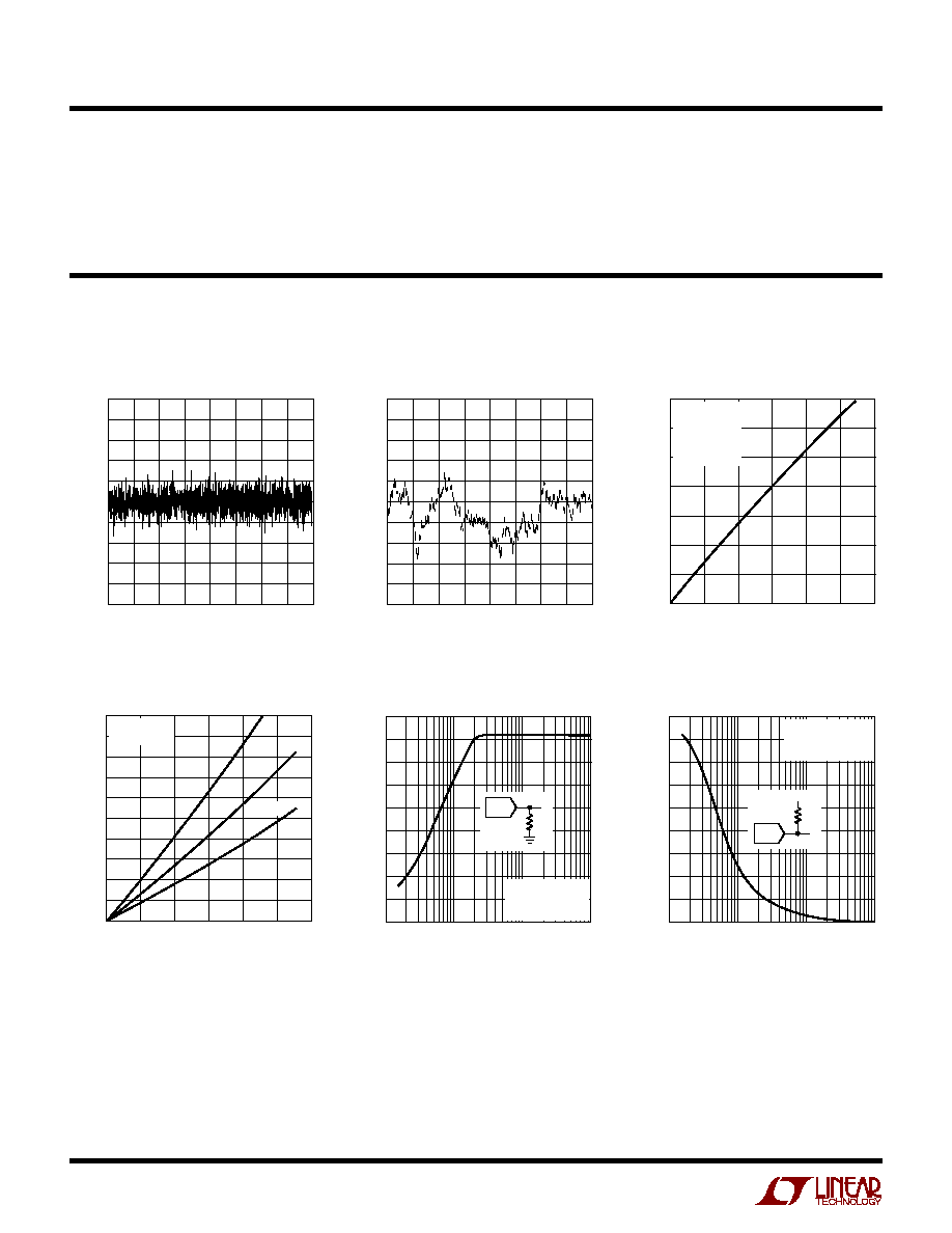
Integral Nonlinearity (INL)
LTC1458
Differential Nonlinearity (DNL)
CODE
0
DNL (LSB)
0.5
0.4
0.3
0.2
0.1
0
0.1
0.2
0.3
0.4
0.5
1024
2048 2560
1458 G09
512
1536
3072 3584 4095
CODE
0
INL ERROR (LSB)
2.0
1.6
1.2
0.8
0.4
0
0.4
0.8
1.2
1.6
2.0
1024
2048 2560
1458 G08
512
1536
3072 3584 4095
Minimum Supply Headroom for
Full Output Swing vs Load Current
LOAD CURRENT (mA)
V
CC
V
OUT
(V)
1.4
1.2
1.0
0.8
0.6
0.4
0.2
0
1458 G03
0
V
OUT
< 1LSB
REFLO = GND
X1/X2 = GND
CODE: ALL 1's
V
OUT
= 4.095V
5
10
15
20
25
30
Minimum Output Voltage vs
Output Sink Current
Output Swing vs Load Resistance
LOAD RESISTANCE (
)
10
OUTPUT SWING (V)
4.5
4.0
3.5
3.0
2.5
2.0
1.5
1.0
0.5
0
100
1k
10k
1458 G05A
R
L
REFLO = GND
X1/X2 = GND
DAC CODE = FFF
H
LOAD RESISTANCE (
)
10
OUTPUT SWING (V)
4.5
4.0
3.5
3.0
2.5
2.0
1.5
1.0
0.5
0
100
1k
10k
1458 G06A
REFLO = GND
X1/X2 = GND
DAC CODE = OOO
H
R
L
V
CC
OUTPUT SINK CURRENT (mA)
OUTPUT PULL-DOWN VOLTAGE (mV)
1000
900
800
700
600
500
400
300
200
100
0.1
1458 G04
0
REFLO = GND
X1/X2 = GND
125
°
C
55
°
C
25
°
C
5
10
15
20
25
30
Output Swing vs Load Resistance
ELECTRICAL CHARACTERISTICS
TYPICAL PERFOR A CE CHARACTERISTICS
U
W

5
LTC1458/LTC1458L
TEMPERATURE (
°
C)
55
SFULL-SCALE VOLTAGE (V)
25
5
1458 G06
95
125
4.110
4.105
4.100
4.095
4.090
4.085
4.080
35
65
LTC1458 Full-Scale Voltage vs
Temperature
TEMPERATURE (
°
C)
55
OFFSET VOLTAGE (mV)
25
5
1458 G07
95
125
5
4
3
2
1
0
1
2
3
4
5
35
65
LTC1458
Offset Voltage vs Temperature
TEMPERATURE (
°
C)
55
SUPPLY CURRENT (
µ
A)
25
5
1458 G05
95
125
950
940
930
920
910
900
890
880
870
860
850
35
65
V
CC
= 5.5V
V
CC
= 5V
V
CC
= 4.5V
LTC1458
Supply Current vs Temperature
X1/X2 C, X1/X2 D,X1/X2 A, X1/X2 B (Pins 1, 14, 16, 27):
The Input Pin that Sets the Gain for DAC C/D/A/B. When
grounded the gain will be 2, i.e., output full-scale will be
2 · REFHI. When connected to V
OUT
the gain will be 1, i.e.,
output full-scale will be equal to REFHI.
V
OUT C
,
V
OUT D
,
V
OUT A
,
V
OUT B
(Pins 2, 13, 17, 26): The
Buffered DAC Outputs.
CS/LD (Pin 3): The Serial Interface Enable and Load
Control Input.
D
IN
(Pin 4): The Serial Data Input.
REFHI C, REFHI D, REFHI A, REFHI B,(Pins 5, 9, 20, 24):
The Inputs to the DAC Resistor Ladder for DAC C/D/A/B.
GND (Pins 6, 23): Ground.
REFLO C, REFLO D, REFLO A, REFLO B, (Pins 7, 8, 21,
22): The Bottom of the DAC Resistor Ladders for the
DACs. These can be used to offset zero-scale above
ground. REFLO should be connected to ground when no
offset is required.
D
OUT
(Pin 10): The Output of the Shift Register which
Becomes Valid on the Rising Edge of the Serial Clock.
CLK (Pin 11): The Serial Interface Clock Input.
V
CC
(Pins 15, 28): The Positive Supply Input. 4.5V
V
CC
5.5V (LTC1458), 2.7V
V
CC
5.5V (LTC1458L). Re-
quires a 0.1
µ
F bypass capacitor to ground.
REFOUT (Pin 19): The Output of the Internal Reference.
CLR (Pin 25): The Clear Pin. Clears all DACs to zero-scale
when pulled low.
TYPICAL PERFOR A CE CHARACTERISTICS
U
W
U
U
U
PI FU CTIO S