 | ÐлекÑÑоннÑй компоненÑ: LTC1518IS | СкаÑаÑÑ:  PDF PDF  ZIP ZIP |
15189fa.pm6
1
LTC1518/LTC1519
52Mbps Precision Delay
RS485 Quad Line Receivers
s
Precision Propagation Delay: 18.5ns
±
3.5ns Over
0
°
C to 70
°
C Temperature Range
s
High Data Rate:
52Mbps
s
Low t
PLH
/t
PHL
Skew: 500ps Typ
s
Low Channel-to-Channel Skew: 500ps Typ
s
Guaranteed Fail-Safe Operation over the Entire
Common Mode Range
s
7V to 12V RS485 Input Common Mode Range
s
Input Resistance
22k, Even When Unpowered
s
Hot Swap
TM
Capable
s
High Common Mode Rejection to 26MHz
s
Short-Circuit Protection: 10mA Typ Output Current
for an Indefinite Short
s
Three-State Output Capability
s
Will Not Oscillate with Slow Moving Input Signals
s
Single 5V Supply
s
Pin Compatible with LTC488, LTC489
The LTC
®
1518/LTC1519 are high speed, precision delay
differential quad bus/line receivers that can operate at data
rates as high as 52Mbps. They are pin compatible with the
LTC488/LTC489 RS485 line receivers and operate over the
entire 7V to 12V common mode range. A unique architec-
ture provides very stable propagation delays and low skew
over wide input common mode, input overdrive and ambi-
ent temperature ranges. Propagation delay is 18.5ns
±
3.5ns
over the commercial temperature range. Typical t
PLH
/t
PHL
and channel-to-channel skew is 500ps.
Each receiver translates differential input levels (
V
ID
300mV) into valid CMOS and TTL output levels. Its high
input resistance (
22k) allows many receivers to be con-
nected to the same driver. The receiver outputs go into a
high impedance state when disabled.
The receivers have a fail-safe feature that guarantees a high
output state when the inputs are shorted or left floating.
Other protection features include thermal shutdown and a
controlled maximum short-circuit current (50mA Max).
Input resistance remains
22k when the device is
unpowered or disabled, thus allowing hot swapping with-
out loading the data lines.
The LTC1518/LTC1519 operate from a single 5V supply
and draw 12mA of supply current.
s
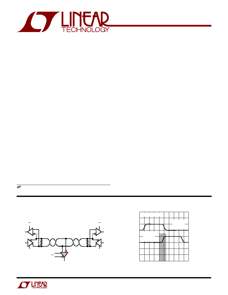
High Speed RS485/RS422 Receivers
s
STS-1/OC-1 Data Receivers
s
PECL Line Receivers
s
Level Translators
s
Fast-20/Fast-40 SCSI Receiver
Propagation Delay Guaranteed to Fall
Within Shaded Area (
±
3.5ns)
52Mbps Data Communication over Twisted Pair
, LTC and LT are registered trademarks of Linear Technology Corporation.
Hot Swap is a trademark of Linear Technology Corporation.
FEATURES
DESCRIPTIO
U
APPLICATIO S
U
TYPICAL APPLICATIO
U
1518/19 TA02
V
IN
=
3V/DIV
V
OUT
=
5V/DIV
5
5
15
TIME (ns)
25
35
0
10
20
30
40 45
RECEIVER
INPUT
V
ID
= 1.5V
RECEIVER
OUTPUT
V
DD
= 5V
T
A
= 0
°
C TO 70
°
C
100
A 1
4
EN
EN
RO
1518/19 F08
1/4 LTC1518
LTC1685
LTC1685
12
3
2 B
7
6
3
2
DE
DI
RO
4
1
100
7
6
3
2
DE
DI
RO
4
1
RE
RE
2
LTC1518/LTC1519
(Note 1)
Supply Voltage ....................................................... 10V
Digital Input Currents ..................... 100mA to 100mA
Digital Input Voltages ............................... 0.5V to 10V
Receiver Input Voltages ........................................
±
14V
Receiver Output Voltages ............. 0.5V to V
DD
+ 0.5V
Receiver Input Differential ....................................... 10V
Short-Circuit Duration .................................... Indefinite
Operating Temperature Range
LTC1518C/LTC1519C ............................. 0
°
C to 70
°
C
LTC1518I/LTC1519I .......................... 40
°
C to 85
°
C
Storage Temperature Range ................ 65
°
C to 150
°
C
Lead Temperature (Soldering, 10 sec)................. 300
°
C
T
JMAX
= 150
°
C,
JA
= 90
°
C/ W
Consult factory for Military grade parts.
ORDER PART
NUMBER
LTC1518CS
LTC1518IS
ORDER PART
NUMBER
LTC1519CS
LTC1519IS
T
JMAX
= 150
°
C,
JA
= 90
°
C/ W
SYMBOL
PARAMETER
CONDITIONS
MIN
TYP
MAX
UNITS
V
CM
Input Common Mode Voltage
A, B Inputs
q
7
12
V
V
IH
Input High Voltage
EN, EN, EN12, EN34
q
2
V
V
IL
Input Low Voltage
EN, EN, EN12, EN34
q
0.8
V
I
IN1
Input Current
EN, EN, EN12, EN34
q
1
1
µ
A
I
IN2
Input Current (A, B)
V
A
, V
B
= 12V
q
500
µ
A
V
A
, V
B
= 7V
q
500
µ
A
R
IN
Input Resistance
7V
V
CM
12V (Figure 5)
q
22
k
C
IN
Input Capacitance
(Note 4)
3
pF
V
OC
Open-Circuit Input Voltage
V
DD
= 5V (Note 4) (Figure 5)
q
3.2
3.3
3.4
V
V
ID(MIN)
Differential Input Threshold Voltage
7V
V
CM
12V
q
0.3
0.3
V
dV
ID
Input Hysteresis
V
CM
= 2.5V
25
mV
V
OH
Output High Voltage
I
OUT
= 4mA, V
ID
= 0.3V, V
DD
= 5V
q
4.6
V
V
OL
Output Low Voltage
I
OUT
= 4mA, V
ID
= 0.3V, V
DD
= 5V
q
0.4
V
I
OZR
Three-State Output Current
0V < V
OUT
< 5V
q
10
10
µ
A
I
DD
Total Supply Current All 4 Receivers
V
ID
> 0.3V, No Load, Device Enabled
q
12
20
mA
I
OSR
Short-Circuit Current
V
OUT
= 0V, V
OUT
= 5V (Note 7)
q
50
50
mA
The
q
denotes specifications which apply over the full operating
temperature range, otherwise specifications are at T
A
= 25
°
C. V
DD
= 5V
±
5% (Notes 2, 3) per receiver, unless otherwise noted.
ABSOLUTE AXI U RATI GS
W
W
W
U
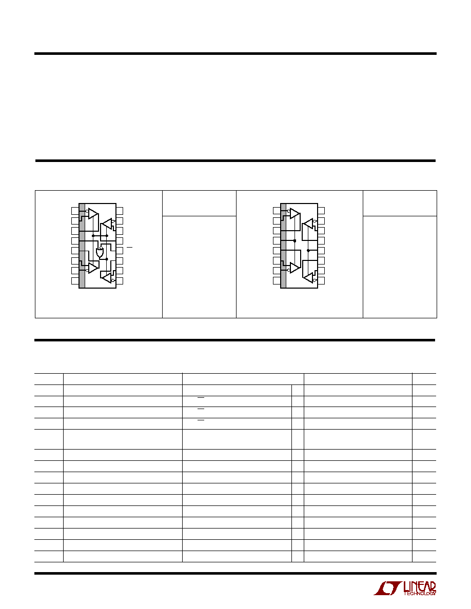
PACKAGE/ORDER I FOR ATIO
U
U
W
TOP VIEW
S PACKAGE
16-LEAD PLASTIC SO
1
2
3
4
5
6
7
8
16
15
14
13
12
11
10
9
B1
A1
OUT 1
EN
OUT 2
A2
B2
GND
V
DD
B4
A4
OUT 4
EN
OUT 3
A3
B3
TOP VIEW
S PACKAGE
16-LEAD PLASTIC SO
1
2
3
4
5
6
7
8
16
15
14
13
12
11
10
9
B1
A1
OUT 1
EN12
OUT 2
A2
B2
GND
V
DD
B4
A4
OUT 4
EN34
OUT 3
A3
B3
DC ELECTRICAL CHARACTERISTICS
3
LTC1518/LTC1519
SYMBOL
PARAMETER
CONDITIONS
MIN
TYP
MAX
UNITS
Max V
ID
for Fail-Safe Detection
7V
V
CM
12V
25
mV
Min Time to Detect Fault Condition
2
µ
s
CMRR
Common Mode Rejection Ratio
V
CM
= 2.5V, f = 26MHz (Note 4)
45
dB
SYMBOL
PARAMETER
CONDITIONS
MIN
TYP
MAX
UNITS
t
PLH
, t
PHL
Input-to-Output Propagation Delay
C
L
= 15pF, 0
°
C
T
A
70
°
C (Figure 1)
q
15
18.5
22
ns
C
L
= 15pF, 40
°
C
T
A
85
°
C (Figure 1)
q
12
25
ns
t
r
, t
f
Rise/Fall Times
C
L
= 15pF
2.5
ns
t
SKD
t
PLH
t
PHL
Skew
C
L
= 15pF, Same Receiver (Note 5)
500
ps
t
ZL
Enable to Output Low
C
L
= 15pF, 0
°
C
T
A
70
°
C (Figure 2)
q
10
35
ns
C
L
= 15pF, 40
°
C
T
A
85
°
C (Figure 2)
15
ns
t
ZH
Enable to Output High
C
L
= 15pF, 0
°
C
T
A
70
°
C (Figure 2)
q
10
35
ns
C
L
= 15pF, 40
°
C
T
A
85
°
C (Figure 2)
15
ns
t
LZ
Disable from Output Low
C
L
= 15pF, 0
°
C
T
A
70
°
C (Figure 2)
q
20
35
ns
C
L
= 15pF, 40
°
C
T
A
85
°
C (Figure 2)
25
ns
t
HZ
Disable from Output High
C
L
= 15pF, 0
°
C
T
A
70
°
C (Figure 2)
q
20
35
ns
C
L
= 15pF, 40
°
C
T
A
85
°
C (Figure 2)
25
ns
t
CH-CH
Channel-to-Channel Skew
C
L
= 15pF (Figure 3, Note 6)
500
ps
t
PKG-PKG
Package-to-Package Skew
C
L
= 15pF, Same Temperature
1.5
ns
(Figure 4, Note 4)
t
r
, t
f
Input
Maximum Input Rise or Fall Time
(Note 4)
q
2000
ns
Minimum Input Pulse Width
0
°
C
T
A
70
°
C (Note 4)
q
12
19.2
ns
40
°
C
T
A
85
°
C (Note 4)
q
16
25
ns
f
IN(MAX)
Maximum Input Frequency
Square Wave, 0
°
C
T
A
70
°
C (Note 4)
q
26
40
MHz
Square Wave, 40
°
C
T
A
85
°
C (Note 4)
q
20
30
MHz
Maximum Data Rate
0
°
C
T
A
70
°
C (Note 4)
q
52
80
Mbps
40
°
C
T
A
85
°
C (Note 4)
q
40
65
Mbps
C
L
Load Capacitance
(Note 4)
500
pF
The
q
denotes specifications which apply over the full operating temperature range, otherwise specifications are at T
A
= 25
°
C.
V
DD
= 5V
±
5% (Notes 2, 3) V
ID
= 1.5V, V
CM
= 2.5V, unless otherwise noted.
Note 1: Absolute Maximum Ratings are those values beyond which the life
of a device may be impaired.
Note 2: All currents into the device pins are positive; all currents out of the
device pins are negative.
Note 3: All typicals are given for V
DD
= 5V, T
A
= 25
°
C.
Note 4: Guaranteed by design, but not tested.
Note 5: Worst-case
t
PLH
t
PHL
skew for a single receiver in a package
over the full operating temperature range.
Note 6: Maximum difference between any two t
PLH
or t
PHL
transitions in a
single package over the full operating temperature range.
Note 7: Short-circuit current does not represent output drive capability.
When the output detects a short-circuit condition, output drive current is
significantly reduced until the short is removed.
The
q
denotes specifications which apply over the full operating
temperature range, otherwise specifications are at T
A
= 25
°
C. V
DD
= 5V
±
5% (Notes 2, 3) per receiver, unless otherwise noted.
DC ELECTRICAL CHARACTERISTICS
SWITCHI G TI E CHARACTERISTICS
U
W
4
LTC1518/LTC1519
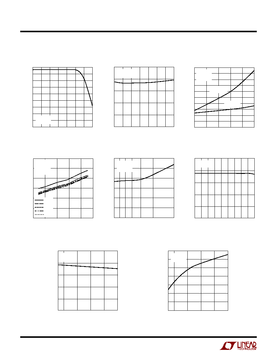
CMRR vs Frequency
Supply Current vs Data Rate
Supply Current
vs Temperature and Data Rate
Propagation Delay
vs Common Mode
Maximum Data Rate
vs Input Differential Voltage
Propagation Delay
vs Load Capacitance
Propagation Delay (t
PLH
/t
PHL
)
vs Temperature
Propagation Delay
vs Input Differential Voltage
FREQUENCY (Hz)
10
42.0
COMMON MODE REJECTION RATIO (dB)
42.5
43.5
44.0
44.5
46.5
15189 G01
43.0
1k
100k
10M
45.0
45.5
46.0
T
A
= 25
°
C
V
CM
= 2.5V
TEMPERATURE (
°
C)
50
25
0
PROPAGATION DELAY (ns)
10
25
0
50
75
15189 G02
5
20
15
25
100
125
V
CM
= 2.5V
V
ID
= 1.5V
DATA RATE (Mbps)
0
SUPPLY CURRENT (mA)
50
45
40
35
30
25
20
15
10
5
0
40
15189 G03
10
20
30
50
T
A
= 25
°
C
V
CM
= 2.5V
V
ID
= 1.5V
4 RECEIVERS
SWITCHING
1 RECEIVER
SWITCHING
DATA RATE (Mbps)
0
SUPPLY CURRENT (mA)
30
25
20
15
10
5
0
40
15189 G04
10
20
30
50
V
CM
= 2.5V
V
ID
= 1.5V
1 RECEIVER
SWITCHING
100
°
C
25
°
C
0
°
C
25
°
C
50
°
C
LOAD CAPACITANCE (pF)
5
15 25
35
55
105
205
PROPAGATION DELAY (ns)
30
25
20
15
10
5
0
15189 G05
T
A
= 25
°
C
V
CM
= 2.5V
V
ID
= 1.5V
COMMON MODE (V)
6
PROPAGATION DELAY (ns)
25
20
15
10
5
0
2
2
4
12
15189 G06
4
0
6
8
10
T
A
= 25
°
C
V
ID
= 1.5V
INPUT DIFFERENTIAL (V)
0.3
PROPAGATION DELAY (ns)
25
20
15
10
5
0
0.5
1.0
1.5
2.0
15189 G07
2.5
T
A
= 25
°
C
V
CM
= 2.5V
INPUT DIFFERENTIAL (V)
0.3
DATA RATE (Mbps)
70
60
50
40
30
20
10
0
0.5
1.0
1.5
2.0
15189 G08
2.5
T
A
= 25
°
C
V
CM
= 2.5V
TYPICAL PERFOR A CE CHARACTERISTICS
U
W

5
LTC1518/LTC1519
LTC1518
B1 (Pin 1): Receiver 1 Inverting Input.
A1 (Pin 2): Receiver 1 Noninverting Input.
OUT 1 (Pin 3): Receiver 1 Output.
EN (Pin 4): A high enables all outputs; a low on Pin 4 and
a high on Pin 12 will put all outputs into a high impedance
state. Do not float.
OUT 2 (Pin 5): Receiver 2 Output.
A2 (Pin 6): Receiver 2 Noninverting Input.
B2 (Pin 7): Receiver 2 Inverting Input.
GND (Pin 8): Ground Pin. A ground plane is recommended
for all LTC1518 applications.
B3 (Pin 9): Receiver 3 Inverting Input.
A3 (Pin 10): Receiver 3 Noninverting Input.
OUT 3 (Pin 11): Receiver 3 Output.
EN (Pin 12): A low enables all outputs; a low on Pin 4 and
a high on Pin 12 will put all outputs into a high impedance
state. Do not float.
OUT 4 (Pin 13): Receiver 4 Output.
A4 (Pin 14): Receiver 4 Noninverting Input.
B4 (Pin 15): Receiver 4 Inverting Input.
V
DD
(Pin 16): Power Supply Input. This pin should be
decoupled with a 0.1
µ
F ceramic capacitor as close as
possible to the pin. Recommended: V
DD
= 5V
±
5%.
LTC1519
B1 (Pin 1): Receiver 1 Inverting Input.
A1 (Pin 2): Receiver 1 Noninverting Input.
OUT 1 (Pin 3): Receiver 1 Output.
EN12 (Pin 4): A high enables receivers 1 and 2; a low will
put the outputs of receivers 1 and 2 into a high impedance
state. Do not float.
OUT 2 (Pin 5): Receiver 2 Output.
A2 (Pin 6): Receiver 2 Noninverting Input.
B2 (Pin 7): Receiver 2 Inverting Input.
GND (Pin 8): Ground Pin. A ground plane is recommended
for all LTC1519 applications.
B3 (Pin 9): Receiver 3 Inverting Input.
A3 (Pin 10): Receiver 3 Noninverting Input.
OUT 3 (Pin 11): Receiver 3 Output.
EN34 (Pin 12): A high enables receivers 3 and 4; a low will
put the outputs of receivers 3 and 4 into a high impedance
state. Do not float.
OUT 4 (Pin 13): Receiver 4 Output.
A4 (Pin 14): Receiver 4 Noninverting Input.
B4 (Pin 15): Receiver 4 Inverting Input.
V
DD
(Pin 16): Power Supply Input. This pin should be
decoupled with a 0.1
µ
F ceramic capacitor as close as
possible to the pin. Recommended: V
DD
= 5V
±
5%.
U
U
U
PI FU CTIO S