 | –≠–ª–µ–∫—Ç—Ä–æ–Ω–Ω—ã–π –∫–æ–º–ø–æ–Ω–µ–Ω—Ç: LTC1519CS | –°–∫–∞—á–∞—Ç—å:  PDF PDF  ZIP ZIP |
1
LTC1518/LTC1519
52Mbps Precision Delay
RS485 Quad Line Receivers
100
A 1
4
EN
EN
RO
1518/19 F08
1/4 LTC1518
LTC1685
LTC1685
12
3
2 B
7
6
3
2
DE
DI
RO
4
1
100
7
6
3
2
DE
DI
RO
4
1
RE
RE
DESCRIPTIO
N
U
s
Precision Propagation Delay: 18.5ns
±
3.5ns Over
Temperature
s
High Data Rate:
52Mbps
s
Low t
PLH
/t
PHL
Skew: 500ps Typ
s
Low Channel-to-Channel Skew: 500ps Typ
s
≠7V to 12V RS485 Input Common Mode Range
s
Input Resistance
22k, Even When Unpowered
s
Guaranteed Fail-Safe Operation over the Entire
Common Mode Range
s
Hot Swap
TM
Capable
s
High Common Mode Rejection to 26MHz
s
Short-Circuit Protection: 10mA Typ Output Current
for an Indefinite Short
s
Three-State Output Capability
s
Will Not Oscillate with Slow Moving Input Signals
s
Single 5V Supply
s
Pin Compatible with LTC488, LTC489
FEATURES
The LTC
Æ
1518/LTC1519 are high speed, precision delay
differential quad bus/line receivers that can operate at data
rates as high as 52Mbps. They are pin compatible with the
LTC488/LTC489 RS485 line receivers and operate over the
entire ≠ 7V to 12V common mode range. A unique architec-
ture provides very stable propagation delays and low skew
over wide input common mode, input overdrive and ambi-
ent temperature ranges. Propagation delay is 18.5ns
±
3.5ns. Typical t
PLH
/t
PHL
and channel-to-channel skew is
500ps.
Each receiver translates differential input levels (
V
ID
300mV) into valid CMOS and TTL output levels. Its high
input resistance (
22k) allows many receivers to be con-
nected to the same driver. The receiver outputs go into a
high impedance state when disabled.
The receivers have a fail-safe feature that guarantees a high
output state when the inputs are shorted or left floating.
Other protection features include thermal shutdown and a
controlled maximum short-circuit current (50mA Max).
Input resistance remains
22k when the device is
unpowered or disabled, thus allowing hot swapping with-
out loading the data lines.
The LTC1518/LTC1519 operate from a single 5V supply
and draw 12mA of supply current.
APPLICATIO
N
S
U
s
High Speed RS485/RS422 Receivers
s
STS-1/OC-1 Data Receivers
s
PECL Line Receivers
s
Level Translators
s
Fast-20/Fast-40 SCSI Receiver
Propagation Delay Guaranteed to Fall
Within Shaded Area (
±
3.5ns)
1518/19 TA02
V
IN
=
3V/DIV
V
OUT
=
5V/DIV
≠ 5
5
15
TIME (ns)
25
35
0
10
20
30
40 45
RECEIVER
INPUT
V
ID
= 1.5V
RECEIVER
OUTPUT
V
DD
= 5V
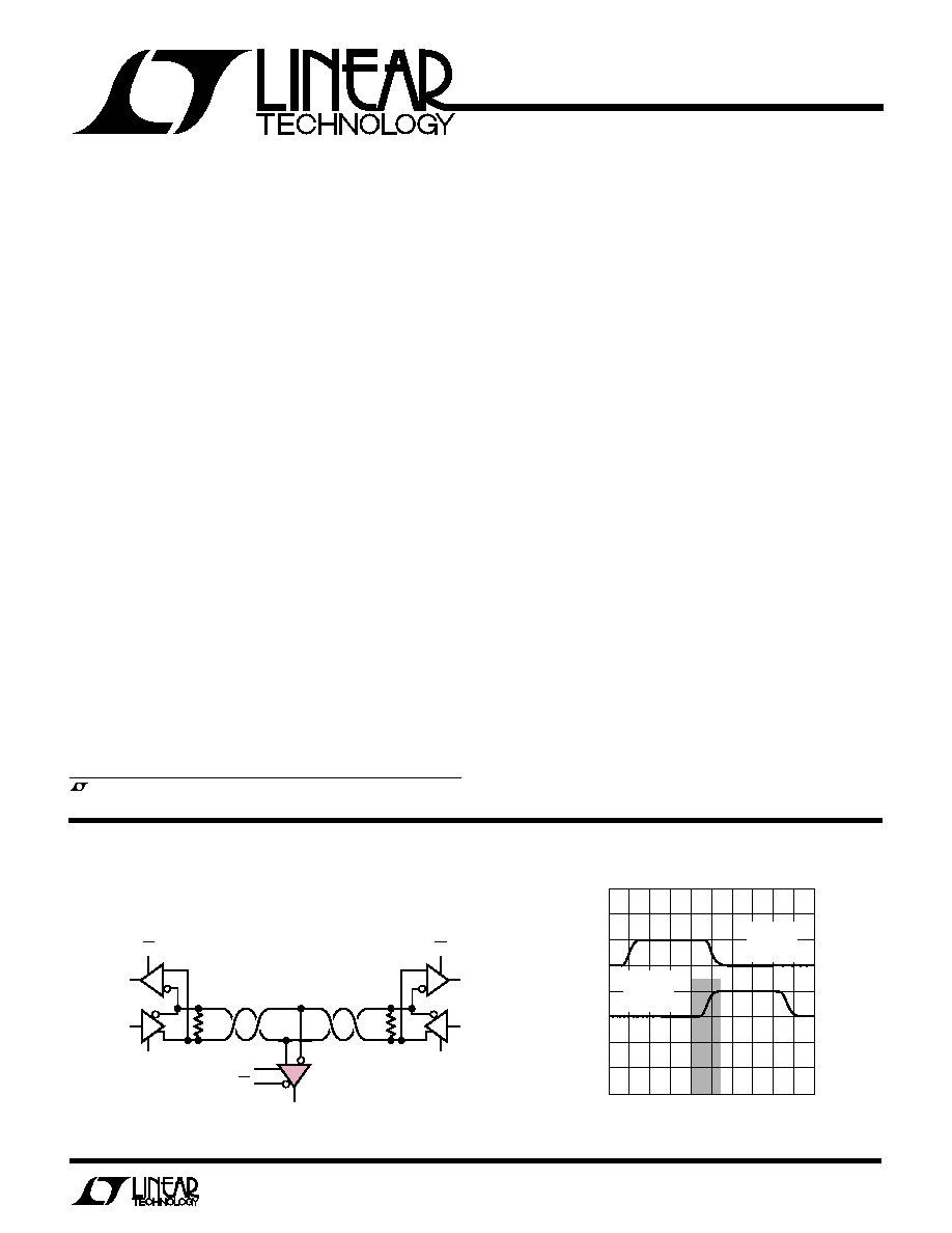
52Mbps Data Communication over Twisted Pair
TYPICAL APPLICATIO
N
U
, LTC and LT are registered trademarks of Linear Technology Corporation.
Hot Swap is a trademark of Linear Technology Corporation.
2
LTC1518/LTC1519
A
U
G
W
A
W
U
W
A
R
BSOLUTE
XI
TI
S
(Note 1)
Supply Voltage ....................................................... 10V
Digital Input Currents ..................... ≠ 100mA to 100mA
Digital Input Voltages ............................... ≠ 0.5V to 10V
Receiver Input Voltages ........................................
±
14V
Receiver Output Voltages ............. ≠ 0.5V to V
DD
+ 0.5V
Receiver Input Differential ....................................... 10V
Short-Circuit Duration .................................... Indefinite
Operating Temperature Range .................... 0
∞
C to 70
∞
C
Storage Temperature Range ................ ≠ 65
∞
C to 150
∞
C
Lead Temperature (Soldering, 10 sec)................. 300
∞
C
W
U
U
PACKAGE/ORDER I FOR ATIO
T
JMAX
= 150
∞
C,
JA
= 90
∞
C/ W
Consult factory for Industrial and Military grade parts.
ORDER PART
NUMBER
LTC1518CS
ORDER PART
NUMBER
LTC1519CS
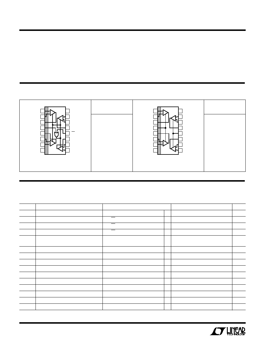
TOP VIEW
S PACKAGE
16-LEAD PLASTIC SO
1
2
3
4
5
6
7
8
16
15
14
13
12
11
10
9
B1
A1
OUT 1
EN
OUT 2
A2
B2
GND
V
DD
B4
A4
OUT 4
EN
OUT 3
A3
B3
T
JMAX
= 150
∞
C,
JA
= 90
∞
C/ W
TOP VIEW
S PACKAGE
16-LEAD PLASTIC SO
1
2
3
4
5
6
7
8
16
15
14
13
12
11
10
9
B1
A1
OUT 1
EN12
OUT 2
A2
B2
GND
V
DD
B4
A4
OUT 4
EN34
OUT 3
A3
B3
DC ELECTRICAL CHARACTERISTICS
SYMBOL
PARAMETER
CONDITIONS
MIN
TYP
MAX
UNITS
V
CM
Input Common Mode Voltage
A, B Inputs
q
≠ 7
12
V
V
IH
Input High Voltage
EN, EN, EN12, EN34
q
2
V
V
IL
Input Low Voltage
EN, EN, EN12, EN34
q
0.8
V
I
IN1
Input Current
EN, EN, EN12, EN34
q
≠ 1
1
µ
A
I
IN2
Input Current (A, B)
V
A
, V
B
= 12V
q
500
µ
A
V
A
, V
B
= ≠ 7V
q
≠ 500
µ
A
R
IN
Input Resistance
≠ 7V
V
CM
12V (Figure 5)
q
22
k
C
IN
Input Capacitance
(Note 4)
3
pF
V
OC
Open-Circuit Input Voltage
V
DD
= 5V (Note 4) (Figure 5)
q
3.2
3.3
3.4
V
V
ID(MIN)
Differential Input Threshold Voltage
≠ 7V
V
CM
12V
q
≠ 0.3
0.3
V
dV
ID
Input Hysteresis
V
CM
= 2.5V
25
mV
V
OH
Output High Voltage
I
OUT
= ≠ 4mA, V
ID
= 0.3V, V
DD
= 5V
q
4.6
V
V
OL
Output Low Voltage
I
OUT
= 4mA, V
ID
= ≠ 0.3V, V
DD
= 5V
q
0.4
V
I
OZR
Three-State Output Current
0V < V
OUT
< 5V
q
≠ 10
10
µ
A
I
DD
Total Supply Current All 4 Receivers
V
ID
> 0.3V, No Load, Device Enabled
q
12
20
mA
I
OSR
Short-Circuit Current
V
OUT
= 0V, V
OUT
= 5V (Note 7)
q
≠ 50
50
mA
V
DD
= 5V
±
5% (Notes 2, 3) per receiver, unless otherwise noted.
3
LTC1518/LTC1519
DC ELECTRICAL CHARACTERISTICS
V
DD
= 5V
±
5% (Notes 2, 3) per receiver, unless otherwise noted.
SYMBOL
PARAMETER
CONDITIONS
MIN
TYP
MAX
UNITS
Max V
ID
for Fail-Safe Detection
≠7V
V
CM
12V
25
mV
Min Time to Detect Fault Condition
2
µ
s
CMRR
Common Mode Rejection Ratio
V
CM
= 2.5V, f = 26MHz (Note 4)
45
dB
SYMBOL
PARAMETER
CONDITIONS
MIN
TYP
MAX
UNITS
t
PLH
, t
PHL
Input-to-Output Propagation Delay
C
L
= 15pF (Figure 1)
q
15
18.5
22
ns
t
r
, t
f
Rise/Fall Times
C
L
= 15pF
2.5
ns
t
SKD
t
PLH
≠ t
PHL
Skew
C
L
= 15pF, Same Receiver (Note 5)
500
ps
t
ZL
Enable to Output Low
C
L
= 15pF (Figure 2)
q
10
35
ns
t
ZH
Enable to Output High
C
L
= 15pF (Figure 2)
q
10
35
ns
t
LZ
Disable from Output Low
C
L
= 15pF (Figure 2)
q
20
35
ns
t
HZ
Disable from Output High
C
L
= 15pF (Figure 2)
q
20
35
ns
t
CH-CH
Channel-to-Channel Skew
C
L
= 15pF (Figure 3, Note 6)
500
ps
t
PKG-PKG
Package-to-Package Skew
C
L
= 15pF, Same Temperature
1.5
ns
(Figure 4, Note 4)
t
r
, t
f
Input
Maximum Input Rise or Fall Time
(Note 4)
q
2000
ns
Minimum Input Pulse Width
(Note 4)
q
12
19.2
ns
f
IN(MAX)
Maximum Input Frequency
Square Wave (Note 4)
q
26
40
MHz
Maximum Data Rate
(Note 4)
q
52
80
Mbps
C
L
Load Capacitance
(Note 4)
500
pF
V
DD
= 5V
±
5% (Notes 2, 3) V
ID
= 1.5V, V
CM
= 2.5V, unless otherwise noted.
SWITCHI G TI E CHARACTERISTICS
U
W
The
q
denotes specifications which apply over the full operating
temperature range.
Note 1: Absolute Maximum Ratings are those values beyond which the life
of a device may be impaired.
Note 2: All currents into the device pins are positive; all currents out of the
device pins are negative.
Note 3: All typicals are given for V
DD
= 5V, T
A
= 25
∞
C.
Note 4: Guaranteed by design, but not tested.
Note 5: Worst-case
t
PLH
≠ t
PHL
skew for a single receiver in a package
over the full operating temperature range.
Note 6: Maximum difference between any two t
PLH
or t
PHL
transitions in a
single package over the full operating temperature range.
Note 7: Short-circuit current does not represent output drive capability.
When the output detects a short-circuit condition, output drive current is
significantly reduced until the short is removed.

4
LTC1518/LTC1519
TYPICAL PERFOR
M
A
N
CE CHARACTERISTICS
U
W
CMRR vs Frequency
Supply Current vs Data Rate
DATA RATE (Mbps)
0
SUPPLY CURRENT (mA)
50
45
40
35
30
25
20
15
10
5
0
40
LTC1518/19 ∑ TPC05
10
20
30
50
T
A
= 25
∞
C
V
CM
= 2.5V
V
ID
= 1.5V
4 RECEIVERS
SWITCHING
1 RECEIVER
SWITCHING
Supply Current
vs Temperature and Data Rate
Propagation Delay
vs Common Mode
COMMON MODE (V)
≠6
PROPAGATION DELAY (ns)
25
20
15
10
5
0
≠2
2
4
12
LTC1464 ∑ TPC08
≠4
0
6
8
10
T
A
= 25
∞
C
V
ID
= 1.5V
Maximum Data Rate
vs Input Differential Voltage
INPUT DIFFERENTIAL (V)
0.3
DATA RATE (Mbps)
70
60
50
40
30
20
10
0
0.5
1.0
1.5
2.0
LTC1518/19 ∑ TPC10
2.5
T
A
= 25
∞
C
V
CM
= 2.5V
FREQUENCY (Hz)
10
42.0
COMMON MODE REJECTION RATIO (dB)
42.5
43.5
44.0
44.5
46.5
1518/19 G01
43.0
1k
100k
10M
45.0
45.5
46.0
T
A
= 25
∞
C
V
CM
= 2.5V
DATA RATE (Mbps)
0
SUPPLY CURRENT (mA)
25
20
15
10
5
0
40
LTC1518/19 ∑ TPC06
10
20
30
50
100
∞
C
25
∞
C
≠25
∞
C
0
∞
C
1 RECEIVER
SWITCHING
V
CM
= 2.5V
V
ID
= 1.5V
Propagation Delay
vs Load Capacitance
LOAD CAPACITANCE (pF)
5
15 25
35
55
105
205
PROPAGATION DELAY (ns)
30
25
20
15
10
5
0
LTC1518/19 ∑ TPC07
T
A
= 25
∞
C
V
CM
= 2.5V
V
ID
= 1.5V
TEMPERATURE (
∞
C)
≠50
≠25
0
PROPAGATION DELAY (ns)
10
25
0
50
75
1518/19 G02
5
20
15
25
100
125
V
CM
= 2.5V
V
ID
= 1.5V
Propagation Delay (t
PLH
/t
PHL
)
vs Temperature
Propagation Delay
vs Input Differential Voltage
INPUT DIFFERENTIAL (V)
0.3
PROPAGATION DELAY (ns)
25
20
15
10
5
0
0.5
1.0
1.5
2.0
LTC1518/19 ∑ TPC09
2.5
T
A
= 25
∞
C
V
CM
= 2.5V

5
LTC1518/LTC1519
PI
N
FU
N
CTIO
N
S
U
U
U
LTC1518
B1 (Pin 1): Receiver 1 Inverting Input.
A1 (Pin 2): Receiver 1 Noninverting Input.
OUT 1 (Pin 3): Receiver 1 Output.
EN (Pin 4): A high enables all outputs; a low on Pin 4 and
a high on Pin 12 will put all outputs into a high impedance
state. Do not float.
OUT 2 (Pin 5): Receiver 2 Output.
A2 (Pin 6): Receiver 2 Noninverting Input.
B2 (Pin 7): Receiver 2 Inverting Input.
GND (Pin 8): Ground Pin. A ground plane is recommended
for all LTC1518 applications.
B3 (Pin 9): Receiver 3 Inverting Input.
A3 (Pin 10): Receiver 3 Noninverting Input.
OUT 3 (Pin 11): Receiver 3 Output.
EN (Pin 12): A low enables all outputs; a low on Pin 4 and
a high on Pin 12 will put all outputs into a high impedance
state. Do not float.
OUT 4 (Pin 13): Receiver 4 Output.
A4 (Pin 14): Receiver 4 Noninverting Input.
B4 (Pin 15): Receiver 4 Inverting Input.
V
DD
(Pin 16): Power Supply Input. This pin should be
decoupled with a 0.1
µ
F ceramic capacitor as close as
possible to the pin. Recommended: V
DD
= 5V
±
5%.
LTC1519
B1 (Pin 1): Receiver 1 Inverting Input.
A1 (Pin 2): Receiver 1 Noninverting Input.
OUT 1 (Pin 3): Receiver 1 Output.
EN12 (Pin 4): A high enables receivers 1 and 2; a low will
put the outputs of receivers 1 and 2 into a high impedance
state. Do not float.
OUT 2 (Pin 5): Receiver 2 Output.
A2 (Pin 6): Receiver 2 Noninverting Input.
B2 (Pin 7): Receiver 2 Inverting Input.
GND (Pin 8): Ground Pin. A ground plane is recommended
for all LTC1519 applications.
B3 (Pin 9): Receiver 3 Inverting Input.
A3 (Pin 10): Receiver 3 Noninverting Input.
OUT 3 (Pin 11): Receiver 3 Output.
EN34 (Pin 12): A high enables receivers 3 and 4; a low will
put the outputs of receivers 3 and 4 into a high impedance
state. Do not float.
OUT 4 (Pin 13): Receiver 4 Output.
A4 (Pin 14): Receiver 4 Noninverting Input.
B4 (Pin 15): Receiver 4 Inverting Input.
V
DD
(Pin 16): Power Supply Input. This pin should be
decoupled with a 0.1
µ
F ceramic capacitor as close as
possible to the pin. Recommended: V
DD
= 5V
±
5%.
6
LTC1518/LTC1519
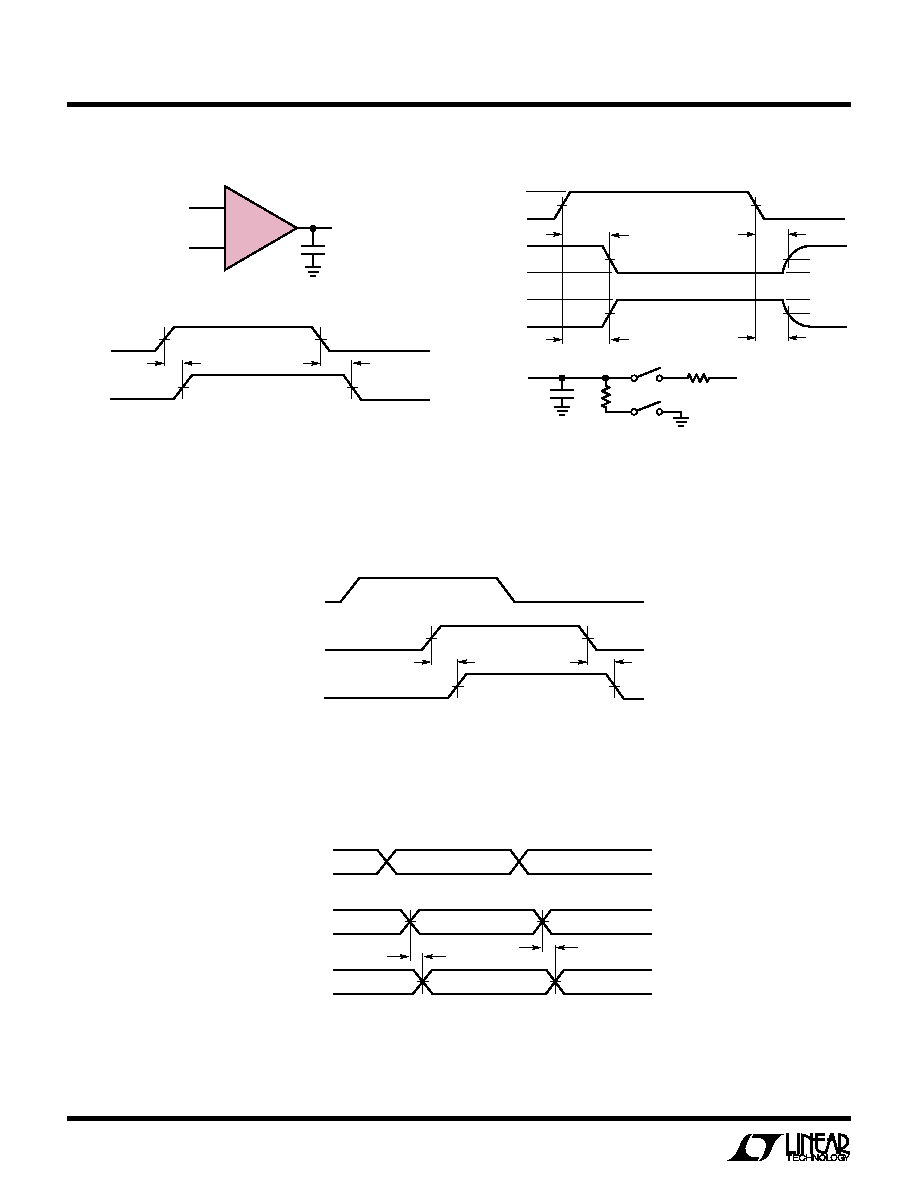
SWITCHI G TI E WAVEFOR S
U
W
W
t
r
= t
f
3ns for all input and enable signals.
Figure 1. Propagation Delay Test Circuit and Waveforms
2.5V
2.5V
V
DD
/2
V
DD
/2
4V
1V
INPUT
OUTPUT
t
PLH
t
PHL
1518/19 F01
≠
+
INPUT
2.5V
OUTPUT
15pF
1518/19 F01b
1/4
LTC1518
LTC1519
Figure 2. Receiver Enable and Disable Timing Test Circuit
and Waveforms
SAME INPUT FOR BOTH PACKAGES
INPUT
A1, B1
V
ID
= 1.5V
PACKAGE 1
OUT 1
1518/19 F04
t
PKG-PKG
t
PKG-PKG
PACKAGE 2
OUT 1
Figure 4. Package-to-Package Propagation Delay Skew
V
DD
/2
V
DD
/2
V
DD
/2
V
DD
/2
4V
B1, B2 = 2.5V
1V
CH1 OUT
INPUT
A1, A2
CH2 OUT
t
CH-CH
t
CH-CH
1518/19 F03
Figure 3. Any Channel to Any Channel Skew, Same Package
1.5V
2.5V
2.5V
C
L
1k
1k
S1
S2
t
ZH
t
ZL
1.5V
t
LZ
0.2V
0.2V
t
HZ
V
DD
OUTPUT
NORMALLY LOW
OUTPUT
NORMALLY HIGH
0V
3V
ENABLE
5V
V
OL
V
OH
0V
RECEIVER
OUTPUT
OUT 1
OUT 1
1518/19 F02

7
LTC1518/LTC1519
EQUIVALE T I PUT NETWORKS
U U
3.3V
22k
22k
A
B
RECEIVER ENABLED, V
DD
= 5V
RECEIVER DISABLED OR V
DD
= 0V
3.3V
22k
A
B
1518/19 F05
22k
Figure 5. Input Thevenin Equivalent
APPLICATIO
N
S I
N
FOR
M
ATIO
N
W
U
U
U
Theory of Operation
Unlike typical line receivers whose propagation delay can
vary by as much as 500% from package to package and
show significant temperature drift, the LTC1518/LTC1519
employ a novel architecture that produces a tightly con-
trolled and temperature compensated propagation delay.
The differential timing skew is also minimized between
rising and falling output edges, and the propagation delays
of any two receivers within a package are very tightly
matched.
The precision timing features of the LTC1518/LTC1519
reduce overall system timing constraints by providing a
narrow
±
3.5ns window during which valid data appears at
the receiver output. This output timing window applies to
all receivers in all packages over all operating tempera-
tures, thereby making the LTC1518/LTC1519 well suited
for high speed data transmission.
In clocked data systems, the low skew minimizes duty
cycle distortion of the clock signal. The LTC1518/LTC1519
can propagate signals at frequencies of 26MHz (52Mbps)
with less than 5% duty cycle distortion. When a clock
signal is used to retime parallel data, the maximum recom-
mended data transmission rate is 25Mbps to avoid timing
errors due to clock distortion.
Thermal shutdown and short-circuit protection prevent
latchup damage to the LTC1518/LTC1519 during fault
conditions.
Fail-Safe Features
The LTC1518/LTC1519 have a fail-safe feature that guar-
antees the output to be in a logic HIGH state when the
inputs are either shorted or left open (note that when
inputs are left open, any external large leakage current
might override the fail-safe). The fail-safe feature detects
shorted inputs over the entire common mode range. When
a fault is detected, the output will typically go high in 2
µ
s.
When some of the receivers within a package are not
used, the open fail-safe feature will allow the user to let
the receiver inputs float and maintain a high logic state at
the output. Without the open fail-safe feature, any noise
at the input would cause unwanted glitches at the output.
When the inputs are left "open," one must make sure that
there are no sources of leakage current connected to one
or both of the inputs. This can happen if the device is
being driven single-endedly and both the signal and the
DC bias are disconnected. If the capacitor used to bypass
the DC bias is left connected to the input of the device and
is leaky (>1
µ
A), the output of the device might not be the
desired high logic state. Also keep in mind that the inputs
are high impedance (
22k
). When left open, noisy
traces should be kept away from the receiver inputs to
minimize capacitive coupling of undesired signals. Even
with the open fail-safe feature, for maximum noise
immunity, grounding the negative input of unused re-
ceivers is recommended.
8
LTC1518/LTC1519
APPLICATIO
N
S I
N
FOR
M
ATIO
N
W
U
U
U
When the inputs are accidentally shorted (by cutting
through a cable, for example), the short-circuit fail-safe
feature will guarantee a high output logic level. Note also
that if the line driver is removed and the termination
resistors are left in place, the receiver will see this as a
"short" and output a logic high.
Both of these fail-safe features will keep the receiver from
outputting false data pulses under fault conditions.
Single-Ended Applications
Over short distances, the LTC1518/LTC1519 can be con-
figured to receive single-ended data by tying one input to
a fixed bias voltage and connecting the other input to the
driver output. In such applications, standard high speed
CMOS logic may be used as a driver for the LTC1518/
LTC1519. With a 22k minimum input resistance, the
receiver trip points may be easily adjusted to accommo-
date different driver output swings by changing the resis-
tor divider at the fixed input. Figure 6a shows a single-
ended receiver configuration with the driver and receiver
connected via PC traces. Note that at very high speeds,
transmission line and driver ringing effects must be con-
sidered. Motorola's
MECL System Design Handbook serves
as an excellent reference for transmission line and termi-
nation effects. To mitigate transmission errors and duty
cycle distortion due to driver ringing, a small output filter
or a dampening resistor on the driver's V
DD
may be needed
as shown in Figure 6b. With an open circuit voltage of 3.3V
at both inputs, the receivers can be used without an
external bias applied to the fixed inputs. The fixed input
should be bypassed with a 0.01
µ
F ceramic capacitor. The
positive input should be driven with a 5V CMOS pat in
order to minimize the skew caused by the 3.3V threshold.
Figure 6c shows this configuration. Note that due to the
≠
+
2.2k
5V
PC TRACE
1/4
LTC1518
LTC1519
MC74ACT04
(TTL INPUT)
MC74AC04
(CMOS INPUT)
2.2k
1518/19 F06a
0.01
µ
F
Figure 6a. Single-Ended Receiver
Figure 6b. Techniques to Minimize Driver Ringing
10
PC TRACE OR
PC TRACE
0.01
µ
F
MC74AC04
1518/19 F06b
10pF
10
Figure 6c. Self Biased Single Ended Receiver
≠
+
PC TRACE
1/4
LTC1518
LTC1519
MC74ACT04
(TTL INPUT)
MC74AC04
(CMOS INPUT)
1518/19 F06c
0.01
µ
F

9
LTC1518/LTC1519
APPLICATIO
N
S I
N
FOR
M
ATIO
N
W
U
U
U
increased skew, this configuration might not operate at the
highest data rates. To transmit single-ended data over
short to medium distances, twisted pair is recommended
with the unused wire grounded at both ends (Figure 7).
Differential Transmission
Data rates up to 52Mbps can be transmitted over 100 feet
of high quality category 5 twisted pair. Figure 8 shows the
LTC1518 receiving differential data from an LTC1685
transceiver. As in the single-ended configurations, care
must be taken to properly terminate the differential data
lines to avoid unwanted reflections, etc.
≠
+
1/4
LTC1518
LTC1519
10-FT TWISTED PAIR
MC74ACT04
MC74AC04
0.01
µ
F
100
100
3.3k
5V
5V
1k
1518/19 F07
Figure 7. Medium Distance Single-Ended Transmission
Using a CMOS Driver
100
A 1
4
EN
EN
RO
1518/19 F08
1/4 LTC1518
LTC1685
LTC1685
12
3
2 B
7
6
3
2
DE
DI
RO
4
1
100
7
6
3
2
DE
DI
RO
4
1
RE
RE
Figure 8. LTC1518 Connected to LTC1685
High Speed RS485 Transceiver
10
LTC1518/LTC1519
Figure 9 shows a trace with 100ft category 5 UTP between
an LTC1685 driver and an LTC1518 receiver. Notice that at
the far end of the cable, the signal to the LTC1518 input has
been reduced. Figure 10 shows a 52Mbps square wave.
Output Short-Circuit Protection
The LTC1518/LTC1519 employ voltage sensing short-
circuit protection at the output terminals. For a given input
differential, this circuitry determines what the correct
APPLICATIO
N
S I
N
FOR
M
ATIO
N
W
U
U
U
output level should be. For example, if the input differential
is
300mV, it expects the output to be a logic high. If the
output is subsequently shorted to a voltage below VDD/2,
this circuitry shuts off the output devices and turns on a
smaller device in its place. A timeout period of about 50ns
is used in order to maintain normal high frequency opera-
tion, even under heavy capacitive loads (>100mA tran-
sient current into the load).
Figure 9. 20ns Pulse Propagating Down 100ft of Category 5 UTP
Figure 10. 52Mbps Pulse Train Over 100ft of Category 5 UTP
50ns/DIV
LTC1518/19 ∑ F09
2V/DIV
2V/DIV
5V/DIV
DRIVER
INPUT
RECEIVER
INPUT
RECEIVER
OUTPUT
CABLE
DELAY
NOTES:
TOP TRACE: LTC1685 DRIVER INPUT
MID TRACE: LTC1518 INPUT AT FAR END
OF 100ft CATAGORY 5 UTP
BOTTOM TRACE: LTC1518 OUTPUT
20ns/DIV
LTC1518/19 ∑ F10
1V/DIV
5V/DIV
RECEIVER
INPUT
RECEIVER
OUTPUT
NOTES:
TOP TRACE: LTC1518 INPUT AT FAR END
OF 100ft CAT 5 UTP
BOTTOM TRACE: LTC1518 OUTPUT
11
LTC1518/LTC1519
PACKAGE DESCRIPTIO
N
U
Dimensions in inches (millimeters) unless otherwise noted.
S Package
16-Lead Plastic Small Outline (Narrow 0.150)
(LTC DWG # 05-08-1610)
0.016 ≠ 0.050
0.406 ≠ 1.270
0.010 ≠ 0.020
(0.254 ≠ 0.508)
◊
45
∞
0
∞
≠ 8
∞
TYP
0.008 ≠ 0.010
(0.203 ≠ 0.254)
1
2
3
4
5
6
7
8
0.150 ≠ 0.157**
(3.810 ≠ 3.988)
16
15
14
13
0.386 ≠ 0.394*
(9.804 ≠ 10.008)
0.228 ≠ 0.244
(5.791 ≠ 6.197)
12
11
10
9
S16 0695
0.053 ≠ 0.069
(1.346 ≠ 1.752)
0.014 ≠ 0.019
(0.355 ≠ 0.483)
0.004 ≠ 0.010
(0.101 ≠ 0.254)
0.050
(1.270)
TYP
*DIMENSION DOES NOT INCLUDE MOLD FLASH. MOLD FLASH
SHALL NOT EXCEED 0.006" (0.152mm) PER SIDE
**DIMENSION DOES NOT INCLUDE INTERLEAD FLASH. INTERLEAD
FLASH SHALL NOT EXCEED 0.010" (0.254mm) PER SIDE
Information furnished by Linear Technology Corporation is believed to be accurate and reliable.
However, no responsibility is assumed for its use. Linear Technology Corporation makes no represen-
tation that the interconnection of its circuits as described herein will not infringe on existing patent rights.
12
LTC1518/LTC1519
©
LINEAR TECHNOLOGY CORPORATION 1997
15189fs, sn15189 LT/TP 0298 4K ∑ PRINTED IN THE USA
Linear Technology Corporation
1630 McCarthy Blvd., Milpitas, CA 95035-7417
q
(408) 432-1900
FAX: (408) 434-0507
q
TELEX: 499-3977
q
www.linear-tech.com
RELATED PARTS
PART NUMBER
DESCRIPTION
COMMENTS
LTC486/LTC487
Low Power Quad RS485 Drivers
10Mbps, ≠ 7V to 12V Common Mode Range
LTC488/LTC489
Low Power Quad RS485 Receivers
10Mbps, ≠ 7V to 12V Common Mode Range
LT
Æ
1016
UltraFast
TM
Precision Comparator
Single 5V Supply, 10ns Propagation Delay
LTC1520
High Speed, Precision Quad Differential Line Receiver
52Mbps,
±
100mV Threshold, Rail-to-Rail Common Mode
LTC1685/LTC1686/
High Speed, Precision RS485 Transceivers
52Mbps, Pin Compatible with LTC485/490/491
LTC1687
UltraFast is a trademark of Linear Technology Corporation.
TYPICAL APPLICATIO
N
U
High Speed Receiver with Hot Swap Control
+
8
7
6
5
1
2
3
4
8
ON
V
CC
V
CC
ON/RESET
GND
DATA
BUS
SENSE
GND
TIMER
GATE
FB
RESET
LTC1422
CONNECTOR 2
R1
0.005
BACK
PLANE
PLUG-IN
CARD
R2
10
5%
R3
6.81k
1%
R4
2.43k
1%
3.3k
3.3k
C1
0.1
µ
F
C4
2200
µ
F
V
CC
5V
5A
Q1
MTB56N06V
0.1
µ
F
1518 TA03
C2
0.33
µ
F
RESET
µ
P
16
2
1
6
7
10
9
14
15
8
4
3
5
D7
D6
D5
D4
D3
D2
D1
D0
11
13
LTC1518
+
≠
+
≠
+
≠
+
≠
16
2
1
6
7
10
9
14
15
8
4
3
5
11
13
LTC1518
+
≠
+
≠
+
≠
CONNECTOR 1
+
≠