1535fs.pm6
LTC1535
1
Isolated RS485 Transceiver
, LTC and LT are registered trademarks of Linear Technology Corporation.
The LTC
®
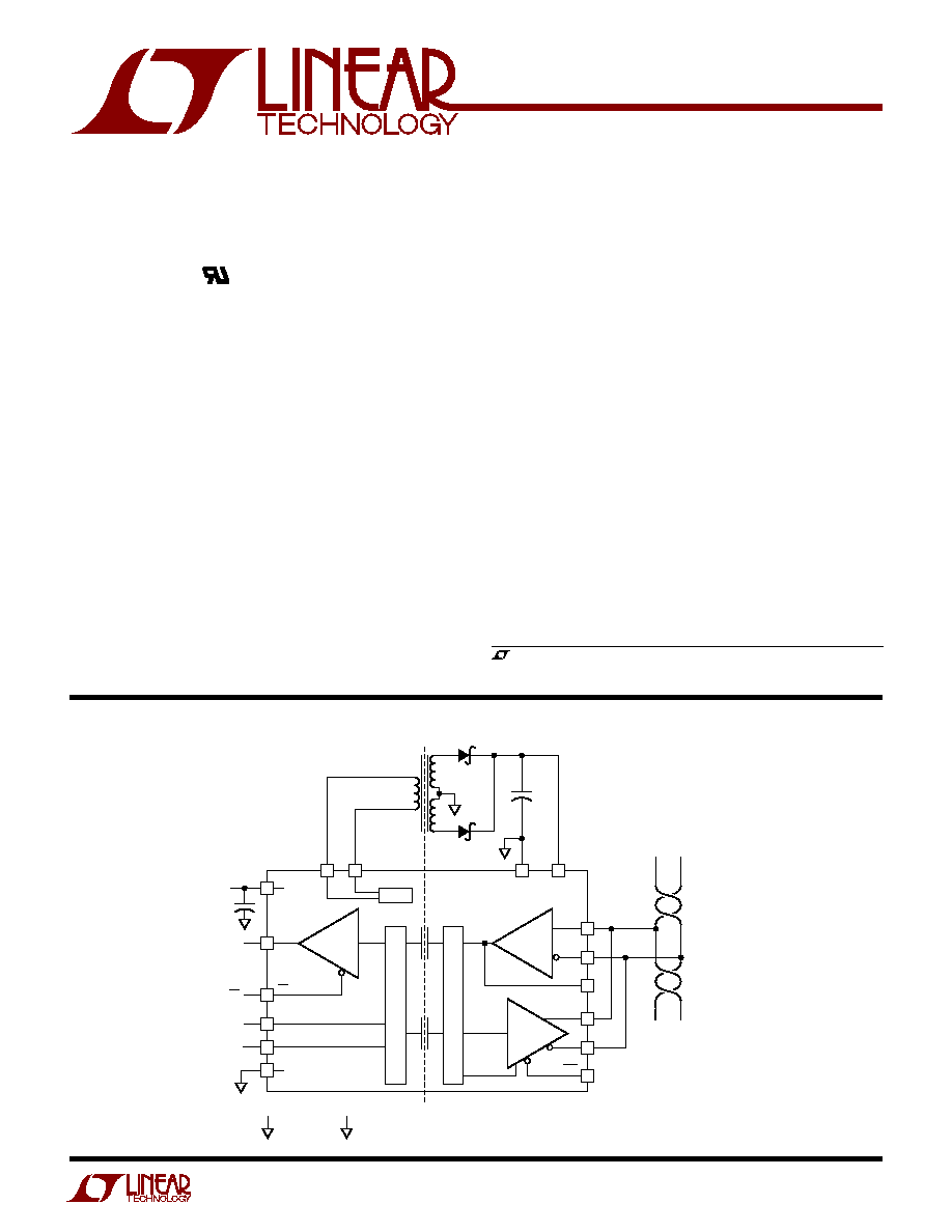
1535 is an isolated RS485 full-duplex differential
line transceiver. Isolated RS485 is ideal for systems where
the ground loop is broken to allow for much larger com-
mon mode voltage ranges. An internal capacitive isolation
barrier provides 2500V
RMS
of isolation between the line
transceiver and the logic level interface. The powered side
contains a 420kHz push-pull converter to power the iso-
lated RS485 transceiver. Internal full-duplex communica-
tion occurs through the capacitive isolation barrier. The
transceiver meets RS485 and RS422 requirements.
The driver and receiver feature three-state outputs, with
the driver maintaining high impedance over the entire
common mode range. The drivers have short-circuit cur-
rent limits in both directions and a slow slew rate select to
minimize EMI or reflections. The 68k
receiver input
allows up to 128 node connections. A fail-safe feature
defaults to a high output state when the receiver inputs are
open or shorted.
s
Isolated RS485 Receiver/Driver
s
RS485 with Large Common Mode Voltage
s
Breaking RS485 Ground Loops
s
Multiple Unterminated Line Taps
s
UL Rated Isolated RS485: 2500V
RMS
UL Recognized
®
File #E151738
s
Half- or Full-Duplex
s
Eliminates Ground Loops
s
250kBd Maximum Data Rate
s
Self-Powered with 420kHz Converter
s
Fail-Safe Output High for Open or
Shorted Receiver Inputs
s
Short-Circuit Current Limit
s
Slow Slew Rate Control
s
68k
Input Impedance Allows Up to 128 Nodes
s
Thermal Shutdown
s
8kV ESD Protection On Driver Outputs and
Receiver Inputs
**
D
Y
Z
SLO
2
1
1
R
A
B
RO2
1535 TA01
V
CC
RO
RE
DE
DI
GND
LOGIC COMMON
2
FLOATING RS485 COMMON
** TRANSFORMER
COOPER (561) 241-7876
420kHz
28
27
26
25
4
17
15
16
18
12
13
14
11
1
+
+
GND2
1/2 BAT54C
1/2 BAT54C
V
CC2
ST1
ST2
3
2
V
CC
RO
RE
DE
DI
1
10
µ
F
10
µ
F
2
CTX02-14659
TWISTED-PAIR
CABLE
APPLICATIO S
U
FEATURES
TYPICAL APPLICATIO
U
DESCRIPTIO
U
2
LTC1535
ORDER PART
NUMBER
LTC1535CSW
LTC1535ISW
T
JMAX
= 125
°
C,
JA
= 125
°
C/W
Consult factory for Military grade parts.
The
q
denotes the specifications which apply over the full operating
temperature range, otherwise specifications are at T
A
= 25
°
C. V
CC
= 5V, V
CC2
= 5V unless otherwise noted.
(Note 1)
SYMBOL
PARAMETER
CONDITIONS
MIN
TYP
MAX
UNITS
V
CC
V
CC
Supply Range
q
4.5
5.5
V
V
CC2
V
CC2
Supply Range
q
4.5
7.5
V
I
CC
V
CC
Supply Current
Transformer Not Driven (Note 10)
q
13
28
mA
I
CC2
V
CC2
Supply Current
R = 27
, Figure 2
q
63
73
mA
No Load
q
7
12
mA
V
OD1
Differential Driver Output
No Load
q
5
V
V
OD2
Differential Driver Output
R = 50
(RS422) (Note 2), V
CC2
= 4.5V
q
2
V
R = 27
(RS485), Figure 2, V
CC2
= 4.5V
q
1.5
2
V
V
OC
Driver Output Common Mode Voltage
DC Level, R = 50
, Figure 2
q
2.0
2.5
3.0
V
I
OSD1
Driver Short-Circuit Current
Driver Enabled (DE = 1)
V
OUT
= HIGH
7V
V
CM
10V
q
60
100
150
mA
V
OUT
= LOW
7V
V
CM
10V
q
60
100
150
mA
V
IH
Logic Input High Voltage
DE, DI, RE
q
2
1.7
V
SLO
q
4
2.2
V
V
IL
Logic Input Low Voltage
DE, DI, RE
q
1.7
0.8
V
SLO
q
1.8
1
V
I
IN
Input Current (A, B)
(Note 3)
V
IN
= 12V
q
0.25
mA
V
IN
= 7V
q
0.20
mA
V
TH
Receiver Input Threshold
7V
V
CM
12V, (Note 4)
q
200
90
10
mV
V
TH
Receiver Input Hysteresis
7V
V
CM
12V
0
°
C
T
A
0
°
C
q
10
30
70
mV
40
°
C
T
A
85
°
C
q
5
30
70
mV
R
IN
Receiver Input Impedance
q
50
68
85
k
1
2
3
4
11
12
13
14
28
27
26
25
18
17
16
15
V
CC
ST1
ST2
GND
GND2
Z
Y
V
CC2
RO
RE
DE
DI
SLO
RO2
A
B
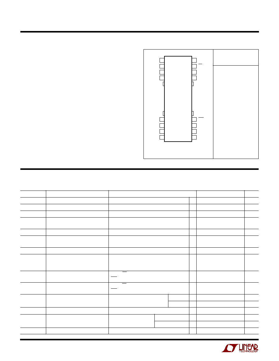
SW PACKAGE
28-LEAD PLASTIC SO
TOP VIEW
ABSOLUTE AXI U
RATI GS
W
W
W
U
PACKAGE/ORDER I FOR ATIO
U
U
W
ELECTRICAL CHARACTERISTICS
V
CC
to GND ................................................................ 6V
V
CC2
to GND2 ............................................................ 8V
Control Input Voltage to GND ...... 0.3V to (V
CC
+ 0.3V)
Driver Input Voltage to GND ........ 0.3V to (V
CC
+ 0.3V)
Driver Output Voltage
(Driver Disabled) to GND2 .............. (V
CC2
13V) to 13V
Driver Output Voltage
(Driver Enabled) to GND2 ............... (V
CC2
13V) to 10V
Receiver Input Voltage to GND2 ............................
±
14V
Receiver Output Voltage .............. 0.3V to (V
CC
+ 0.3V)
Operating Temperature Range
LTC1535C ........................................ 0
°
C
T
A
70
°
C
LTC1535I ..................................... 40
°
C
T
A
85
°
C
Storage Temperature Range ................. 65
°
C to 150
°
C
Lead Temperature (Soldering, 10 sec).................. 300
°
C
LTC1535
3
SYMBOL
PARAMETER
CONDITIONS
MIN
TYP
MAX
UNITS
The
q
denotes the specifications which apply over the full operating
temperature range, otherwise specifications are at T
A
= 25
°
C. V
CC
= 5V, V
CC2
= 5V unless otherwise noted.
V
IOC
Receiver Input Open Circuit Voltage
3.4
V
V
OH
RO Output High Voltage
I
RO
= 4mA, V
CC
= 4.5V
q
3.7
4.0
V
V
OL
RO Output Low Voltage
I
RO
= 4mA, V
CC
= 4.5V
q
0.4
0.8
V
I
OZ
Driver Output Leakage
Driver Disabled (DE = 0)
1
µ
A
V
OH2
RO2 Output High Voltage
I
RO2
= 4mA, V
CC
= 4.5V
q
3.7
3.9
V
V
OL2
RO2 Output Low Voltage
I
RO2
= 4mA, V
CC
= 4.5V
q
0.4
0.8
V
f
SW
DC Converter Frequency
q
290
420
590
kHz
R
SWH
DC Converter Impedance High
q
4
6
R
SWL
DC Converter Impedance Low
q
2.5
5
I
REL
RE Output Low Current
RE Sink Current, Fault = 0
q
40
50
80
µ
A
I
REH
RE Output High Current
RE Source Current, Fault = 1
q
80
100
130
µ
A
V
UVL
Undervoltage Low Threshold
RE Fault = 1, (Note 5)
q
3.90
4.00
4.25
V
V
UVH
Undervoltage High Threshold
RE Fault = 0, (Note 5)
q
4.05
4.20
4.40
V
V
ISO
Isolation Voltage
1 Minute, (Note 6)
2500
V
RMS
1 Second
3000
V
RMS
SYMBOL
PARAMETER
CONDITIONS
MIN
TYP
MAX
UNITS
t
SJ
Data Sample Jitter
Figure 8, (Note 7)
q
250
285
ns
f
MAX
Max Baud Rate
Jitter = 10% Max, SLO = 1, (Note 8)
q
250
410
kBd
t
PLH
Driver Input to Output
DE = 1, SLO = 1, Figure 4, Figure 6
q
600
855
ns
DE = 1, SLO = 0, Figure 4, Figure 6
q
1300
1560
ns
t
PHL
Driver Input to Output
DE = 1, SLO = 1, Figure 4, Figure 6
q
600
855
ns
DE = 1, SLO = 0, Figure 4, Figure 6
q
1300
1560
ns
t
r
, t
f
Driver Rise or Fall Time
DE = 1, SLO = 1, Figure 4, Figure 6
q
20
100
ns
DE = 1, SLO = 0, V
CC
= V
CC2
= 4.5V
q
150
500
1000
ns
t
ZH
Driver Enable to Output
DI = 1, SLO = 1, Figure 5, Figure 7
q
1000
1400
ns
t
ZL
Driver Enable to Output
DI = 0, SLO = 1, Figure 5, Figure 7
q
1000
1400
ns
t
LZ
Driver Disable to Output
DI = 0, SLO = 1, Figure 5, Figure 7
q
700
1300
ns
t
HZ
Driver Disable to Output
DI = 1, SLO = 1, Figure 5, Figure 7
q
700
1300
ns
t
PLH
Receiver Input to RO
RE = 0, Figure 3, Figure 8
q
600
855
ns
t
PHL
Receiver Input to RO
RE = 0, Figure 3, Figure 8
q
600
855
ns
t
PLH
Receiver Input to RO2
RE = 0, Figure 3, Figure 8
30
ns
t
PHL
Receiver Input to RO2
RE = 0, Figure 3, Figure 8
30
ns
t
r
, t
f
Receiver Rise or Fall Time
RE = 0, Figure 3, Figure 8
20
ns
t
LZ
Receiver Disable to Output
Figure 3, Figure 9
30
ns
t
HZ
Receiver Disable to Output
Figure 3, Figure 9
30
ns
t
START
Initial Start-Up Time
(Note 9)
1200
ns
t
TOF
Data Time-Out Fault
(Note 9)
1200
ns
ST1, ST2 Duty Cycle
0
°
C
T
A
70
°
C
q
56
%
40
°
C
T
A
85
°
C
q
57
%
The
q
denotes the specifications which apply over the full operating
temperature range, otherwise specifications are at T
A
= 25
°
C. V
CC
= 5V, V
CC2
= 5V, R = 27
(RS485) unless otherwise noted.
SWITCHI G CHARACTERISTICS
U
ELECTRICAL CHARACTERISTICS
4
LTC1535
Note 1: Absolute Maximum Ratings are those values beyond which the
life of a device may be impaired.
Note 2: RS422 50
specification based on RS485 27
test.
Note 3: I
IN
is tested at V
CC2
= 5V, guaranteed by design from
GND2
V
CC2
5.25V.
Note 4: Input fault conditions on the RS485 receiver are detected with a
fixed receiver offset. The offset is such that an input short or open will
result in a high data output.
Note 5: The low voltage detect faults when V
CC2
or V
CC
drops below V
UVL
and reenables when greater than V
UVH
. The fault can be monitored
through the weak driver output on RE.
Note 6: Value derived from 1 second test.
Note 7: The input signals are internally sampled and encoded. The internal
sample rate determines the data output jitter since the internal sampling is
asynchronous with respect to the external data. Nominally, a 4MHz
internal sample rate gives 250ns of sampling uncertainty in the input
signals.
Note 8: The maximum baud rate is 250kBd with 10% sampling jitter.
Lower baud rates have lower jitter.
Note 9: Start-up time is the time for communication to recover after a fault
condition. Data time-out is the time a fault is indicated on RE after data
communication has stopped.
Note 10. I
CC
measured with no load, ST1 and ST2 floating.
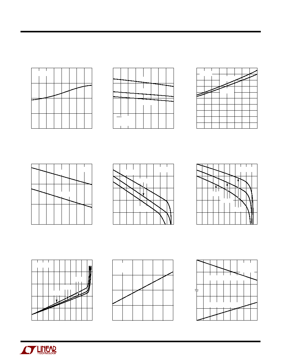
TYPICAL PERFOR A CE CHARACTERISTICS
U
W
TEMPERATURE (
°
C)
50 25
0
25
50
75
100 125 150
V
CC
CURRENT (mA)
1535 G01
130
120
110
100
90
80
70
60
50
R
L
= 54
V
CC
= 5V
COOPER
CTX02-14659
TRANSFORMER
R
L
= 120
R
L
= OPEN
TEMPERATURE (
°
C)
50 25
0
25
50
75
100 125 150
V
CC2
CURRENT (mA)
1535 G02
90
80
70
60
50
40
30
20
10
V
CC2
= 6V
V
CC2
= 5V
V
CC2
= 4.5V
f
DI
= f
MAX
SLO = 0V
R
L
= 54
TEMPERATURE (
°
C)
50 25
0
25
50
75
100 125 150
V
CC2
VOLTAGE (V)
1535 G03
6.5
6.0
5.5
5.0
4.5
R
L
= 54
, V
CC
= 5V
R
L
= 54
, V
CC
= 4.5V
f
DI
= 250kHz
SLO = 0V
COOPER
CTX02-14659
TRANSFORMER
R
L
= OPEN, V
CC
= 5V
TEMPERATURE (
°
C)
50 25
0
25
50
75
100 125 150
f
MAX
(kHz)
1535 G04
500
400
300
200
100
V
CC
= V
CC2
= 4.5V
SLO = V
CC2
R
L
= 54
TEMPERATURE (
°
C)
50 25
0
25
50
75
100 125 150
TIME (ns)
1535 G05
65
60
55
50
45
40
35
30
25
V
CC2
= 5V, 4.5V
SLO = V
CC2
R
L
= 54
TEMPERATURE (
°
C)
50 25
0
25
50
75
100 125 150
TIME (ns)
1535 G06
800
700
600
500
400
300
200
SLO = 0V
R
L
= 54
V
CC2
= 5V
V
CC2
= 4.5V
V
CC
Supply Current vs
Temperature
V
CC2
Supply Current vs
Temperature
V
CC2
Supply Voltage vs
Temperature
Maximum Baud Rate vs
Temperature
Driver Differential Output Rise/
Fall Time vs Temperature
Driver Differential Output Rise/
Fall Time vs Temperature
ELECTRICAL CHARACTERISTICS
LTC1535
5
TYPICAL PERFOR A CE CHARACTERISTICS
U
W
TEMPERATURE (
°
C)
50 25
0
25
50
75
100 125 150
FREQUENCY (kHz)
1535 G07
600
500
400
300
200
V
CC
= 5V
TEMPERATURE (
°
C)
50 25
0
25
50
75
100 125 150
OUTPUT VOLTAGE (V)
1535 G08
4
3
2
1
0
V
CC2
= 6V
V
CC2
= 5V
V
CC2
= 4.5V
SLO = V
CC2
R
L
= 54
TEMPERATURE (
°
C)
50 25
0
25
50
75
100 125 150
OUTPUT VOLTAGE (V)
1535 G09
1.0
0.9
0.8
0.7
0.6
0.5
0.4
0.3
0.2
0.1
0
V
CC
= 5V
V
CC
= 4.5V
I = 8mA
TEMPERATURE (
°
C)
50 25
0
25
50
75
100 125 150
OUTPUT VOLTAGE (V)
1535 G10
4.5
4.0
3.5
3.0
V
CC
= 5V
V
CC
= 4.5V
I = 8mA
OUTPUT CURRENT (mA)
0
10
20
30
40
50
60
70
80
90
OUTPUT VOLTAGE (V)
1535 G11
5
4
3
2
1
0
V
CC
= 5.5V
V
CC
= 4.5V
V
CC
= 5V
T
A
= 25
°
C
OUTPUT CURRENT (mA)
0
10 20 30 40 50 60 70 80 90 100 110
OUTPUT VOLTAGE (V)
1535 G12
5
4
3
2
1
0
V
CC
= 5.5V
V
CC
= 4.5V
V
CC
= 5V
T
A
= 25
°
C
Switcher Frequency vs
Temperature
Driver Differential Output Voltage
vs Temperature
Receiver Output Low Voltage vs
Temperature
Receiver Output High Voltage vs
Temperature
Driver Differential Output Voltage
vs Output Current
Driver Output High Voltage vs
Output Current
OUTPUT CURRENT (mA)
OUTPUT VOLTAGE (V)
1535 G13
5
4
3
2
1
0
V
CC
= 6V
V
CC
= 4.5V
V
CC
= 5V
T
A
= 25
°
C
0
10 20 30 40 50 60 70 80 90 100 110
V
CC2
SUPPLY VOLTAGE (V)
4.5
5
5.5
6
6.5
7
7.5
OUTPUT VOLTAGE (V)
1535 G14
5
4
3
2
1
T
A
= 25
°
C
R
L
= 60
LOAD CURRENT (mA)
0
1
2
3
4
5
6
7
8
9
OUTPUT VOLTAGE (V)
1535 G15
5.0
4.5
4.0
1.0
0.5
0
T
A
= 25
°
C
V
CC
= 5V
OUTPUT HIGH, SOURCING
OUTPUT LOW, SINKING
Driver Output Low Voltage vs
Output Current
Driver Differential Output Voltage
vs V
CC2
Supply Voltage
Receiver Output Voltage vs Load
Current