1
LTC1541/LTC1542
Micropower Op Amp,
Comparator and Reference
Daisy-Chained Control Outputs
FEATURES
The LTC
Æ
1541/LTC1542 combine a micropower ampli-
fier, comparator and bandgap reference (LTC1541) in an
8-pin package. The part operates from a single 2.5V to
12.6V or dual
±
1.25V to
±
6.3V supply with a typical supply
current of 5
µ
A. Both the op amp and comparator feature
a common mode input voltage range that extends from the
negative supply to within 1.3V of the positive supply. The
op amp output stage swings from rail-to-rail. The
comparator's inverting input is internally connected to the
reference output (LTC1541).
The reference output voltage is 1.2V
±
1% over the
extended temperature range. The output can drive a
bypass capacitor of up to 0.01
µ
F without any oscillations.
It can also source up to 2mA and sink up to 20
µ
A.
The op amp is internally compensated to be unity-gain
stable with typical GBW at 12kHz and slew rate of 8V/ms.
The comparator has
±
3mV of internal hysteresis to ensure
clean output switching, even with slow moving input
signals.
The LTC1541/LTC1542 are available in MSOP and SO-8
packages.
DESCRIPTIO
N
U
s
Quiescent Current: 5
µ
A Typ
s
Outputs Swing Rail-to-Rail
s
Low Op Amp Offset Voltage: 700
µ
V Max
s
Reference Output Drives 0.01
µ
F Capacitor
s
Internal 1.2V
±
0.4% Reference Output (LTC1541)
s
Low Input Bias Current: 1nA Max
s
Reference Output Can Source Up to 2mA
s
Internal
±
3mV Comparator Hysteresis
s
Comparator and Op Amp Input Range
Includes Ground
s
Op Amp Capable of Driving Up to 1000pF Load
s
Unity-Gain Stable and 12kHz Bandwidth
s
2.5V to 12.6V Supply Voltage Range
s
Pin Compatible Upgrade for MAX951/MAX953
APPLICATIO
N
S
U
s
Battery- or Solar-Powered Systems
s
Automotive Keyless Entry
s
Low Frequency, Local Area Alarms/Detectors
s
Infrared Receivers for Remote Controls
s
Smoke Detectors and Safety Sensors
s
GSM Portable Phones
TYPICAL APPLICATIO
N
U
, LTC and LT are registered trademarks of Linear Technology Corporation.
Op Amp V
OS
Distribution,
V
CM
= 2.5V, SO-8 Package
Total of 839 Units
INPUT OFFSET VOLTAGE (
µ
V)
≠600
PERCENT OF UNITS (%)
600
1541/42 TA02
≠300
0
300
50
40
30
20
10
0
V
CC
= 5V
V
SS
= 0V
≠
+
1
2
3
7
8
2N3904
SCR LOAD
5
2M
6
2.2
µ
F
1N457
LOW BATTERY
OUTPUT HIGH = "ON"
OUTPUT LOW = "OFF"
1.2V INTERNAL
REFERENCE
1541/42 ∑ TA01
≠
+
10k
VN2222
2M
1M
100k
10M
1k
≠
+
1/2 LTC1541
1/2 LTC1541
10k
I
CC
= 7
µ
A AT V
IN
= 5V
TYPE R
1N457
V
IN
= 3.6V TO 9V
Pilot Light Flame Detector with Low-Battery Lockout
2
LTC1541/LTC1542
ABSOLUTE
M
AXI
M
U
M
RATINGS
W
W
W
U
Supply Voltage ........................................................ 13V
Input Voltage .............................................≠ 0.3V to 13V
Output Voltage ...........................................≠ 0.3V to 13V
Output Short-Circuit Duration .......................... Indefinite
Storage Temperature Range ................. ≠ 65
∞
C to 150
∞
C
Operating Temperature Range
Commercial ............................................. 0
∞
C to 70
∞
C
Industrial ............................................ ≠ 40
∞
C to 85
∞
C
Lead Temperature (Soldering, 10 sec).................. 300
∞
C
W
U
U
PACKAGE/ORDER I FOR ATIO
ORDER PART
NUMBER
T
JMAX
= 125
∞
C,
JA
= 150
∞
C/W
LTC1541CS8
LTC1541IS8
1541
1541I
1
2
3
4
8
7
6
5
TOP VIEW
V
CC
COMPOUT
REF
COMPIN
+
AMPOUT
AMPIN
≠
AMPIN
+
V
SS
S8 PACKAGE
8-LEAD PLASTIC SO
MS8 PART MARKING
ORDER PART
NUMBER
LTC1541CMS8
LTBE
S8 PART MARKING
1
2
3
4
AMPOUT
AMPIN
≠
AMPIN
+
V
SS
8
7
6
5
V
CC
COMPOUT
REF
COMPIN
+
TOP VIEW
MS8 PACKAGE
8-LEAD PLASTIC MSOP
T
JMAX
= 125
∞
C,
JA
= 250
∞
C/W
ORDER PART
NUMBER
T
JMAX
= 125
∞
C,
JA
= 150
∞
C/W
LTC1542CS8
LTC1542IS8
1542
1542I
1
2
3
4
8
7
6
5
TOP VIEW
V
CC
COMPOUT
COMPIN
≠
COMPIN
+
AMPOUT
AMPIN
≠
AMPIN
+
V
SS
S8 PACKAGE
8-LEAD PLASTIC SO
MS8 PART MARKING
ORDER PART
NUMBER
LTC1542CMS8
S8 PART MARKING
1
2
3
4
AMPOUT
AMPIN
≠
AMPIN
+
V
SS
8
7
6
5
V
CC
COMPOUT
COMPIN
≠
COMPIN
+
TOP VIEW
MS8 PACKAGE
8-LEAD PLASTIC MSOP
T
JMAX
= 125
∞
C,
JA
= 250
∞
C/W
LTDE
Consult factory for Military grade parts.
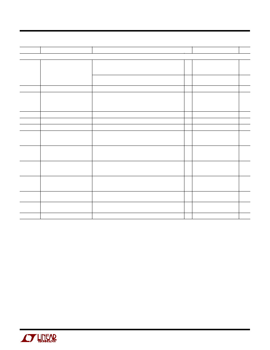
ELECTRICAL CHARACTERISTICS
V
CC
= 5V, V
SS
= 0V, T
A
= 25
∞
C, unless otherwise noted.
SYMBOL
PARAMETER
CONDITIONS
MIN
TYP
MAX
UNITS
Power Supply
V
CC
Supply Voltage Range
q
2.5
12.6
V
I
CC
Supply Current (Note 1)
5
7.5
µ
A
Commercial Grade
q
13
µ
A
Industrial Grade
q
14
µ
A
Comparator
V
OS
Input Offset Voltage (Note 2)
(SO-8)
1
mV
Commercial Grade (SO-8)
q
1.5
mV
Industrial Grade (SO-8)
q
2.0
mV
(MSOP)
1.2
mV
q
2.0
mV
V
TRIP
Trip Point (Note 3)
1.7
2.25
2.8
mV
q
1
3.8
mV
3
LTC1541/LTC1542
ELECTRICAL CHARACTERISTICS
V
CC
= 5V, V
SS
= 0V, T
A
= 25
∞
C, unless otherwise noted.
SYMBOL
PARAMETER
CONDITIONS
MIN
TYP
MAX
UNITS
I
IN
Input Leakage Current (Note 4)
q
0.01
1
nA
V
CM
Input Common Mode Range
q
V
SS
V
CC
≠ 1.3V
V
CMRR
Common Mode Rejection Ratio
V
CM
= V
SS
to (V
CC
≠ 1.3V) (LTC1542)
0.25
mV/V
Commercial Grade
q
0.30
mV/V
Industrial Grade
q
0.35
mV/V
PSRR
Power Supply Rejection Ratio
V
CC
= 3V to 12V
0.25
mV/V
Commercial Grade (SO-8)
q
0.30
mV/V
Industrial Grade (SO-8)
q
0.35
mV/V
t
PD
Propagation Delay
Overdrive = 10mV
20
µ
s
Overdrive = 100mV
8
µ
s
V
OH
Output High Voltage
I
OUT
= ≠ 2mA
q
V
CC
≠ 0.2V
V
V
OL
Output Low Voltage
I
OUT
= 1.8mA
q
V
SS
+ 0.3V
V
Reference (LTC1541 Only)
V
REF
Reference Voltage
No Load (SO-8)
1.195
1.200
1.205
V
Commercial Grade (SO-8)
q
1.190
1.210
V
Industrial Grade (SO-8)
q
1.188
1.212
V
No Load (MSOP)
1.190
1.200
1.210
V
q
1.185
1.215
V
V
REF
Load Regulation
I
SOURCE
= 2mA
q
2
6
mV
I
SINK
= 10
µ
A
0.2
1.5
mV
q
5
mV
e
n
Voltage Noise
0.1Hz to 10Hz
16
µ
V
P-P
Op Amp
V
OS
Input Offset Voltage
V
CM
= 2.5V (SO-8)
0.7
mV
Commercial Grade (SO-8)
q
1.25
mV
Industrial Grade (SO-8)
q
1.65
mV
V
CM
= 2.5V (MSOP)
1.00
mV
q
1.75
mV
I
B
Input Bias Current
V
CM
= 2.5V
q
0.01
1
nA
A
VOL
Large-Signal Gain
AMPOUT = 0.5V to 4.5V, No Load
80
1000
V/mV
AMPOUT = 0.5V to 4.5V, R
LOAD
= 100k
60
500
V/mV
Commercial Grade
q
38
V/mV
Industrial Grade
q
35
V/mV
GBW
Gain Bandwidth
A
V
= 1V/V
12
kHz
SR
Slew Rate
A
V
= 1V/V
8
V/ms
V
CM
Input Common Mode Range
q
V
SS
V
CC
≠ 1.3V
V
CMRR
Common Mode Rejection Ratio
V
CM
= V
SS
to (V
CC
≠ 1.3V)
0.28
mV/V
Commercial Grade
q
0.33
mV/V
Industrial Grade
q
0.38
mV/V
PSRR
Power Supply Rejection Ratio
V
CC
= 3V to 12V
0.19
mV/V
Commercial Grade
q
0.21
mV/V
Industrial Grade
q
0.23
mV/V
V
OH
Output High Voltage
R
LOAD
= 100k to V
SS
V
CC
≠ 0.07
V
Commercial Grade
q
V
CC
≠ 0.10
V
Industrial Grade
q
V
CC
≠ 0.12
V
V
OL
Output Low Voltage
R
LOAD
= 100k to V
SS
V
SS
+ 0.05
V
Commercial Grade
q
V
SS
+ 0.10
V
Industrial Grade
q
V
SS
+ 0.12
V
4
LTC1541/LTC1542
SYMBOL
PARAMETER
CONDITIONS
MIN
TYP
MAX
UNITS
I
SOURCE
Output Source Current
0.9
1.8
mA
q
0.7
mA
I
SINK
Output Sink Current
1.3
1.8
mA
q
0.9
mA
e
n
Input Noise Voltage
f
O
= 0.1Hz to 10Hz
3
µ
V
P-P
ELECTRICAL CHARACTERISTICS
V
CC
= 5V, V
SS
= 0V, T
A
= 25
∞
C, unless otherwise noted.
V
CC
= 3V, V
SS
= 0V, T
A
= 25
∞
C, unless otherwise noted.
SYMBOL
PARAMETER
CONDITIONS
MIN
TYP
MAX
UNITS
Power Supply
V
CC
Supply Voltage Range
q
2.5
12.6
V
I
CC
Supply Current (Note 1)
4.5
7.0
µ
A
Commercial Grade
q
12
µ
A
Industrial Grade
q
13
µ
A
Comparator
V
OS
Input Offset Voltage (Note 2)
(SO-8)
1.0
mV
Commercial Grade (SO-8)
q
1.5
mV
Industrial Grade (SO-8)
q
2.0
mV
(MSOP)
1.2
mV
q
2.0
mV
V
TRIP
Trip Point (Note 3)
1.80
2.35
2.90
mV
q
1.00
3.90
mV
I
IN
Input Leakage Current (Note 4)
q
0.01
1
nA
V
CM
Input Common Mode Range
q
V
SS
V
CC
≠ 1.3
V
CMRR
Common Mode Rejection Ratio
V
CM
= V
SS
to (V
CC
≠ 1.3V) (LTC1542)
0.35
mV/V
Commercial Grade
q
0.40
mV/V
Industrial Grade
q
0.45
mV/V
PSRR
Power Supply Rejection Ratio
V
CC
= 3V to 12V
0.25
mV/V
Commercial Grade
q
0.30
mV/V
Industrial Grade
q
0.35
mV/V
t
PD
Propagation Delay
Overdrive = 10mV
25
µ
s
Overdrive = 100mV
12
µ
s
V
OH
Output High Voltage
I
OUT
= ≠ 2mA
q
V
CC
≠ 0.2
V
V
OL
Output Low Voltage
I
OUT
= 1.8mA
q
V
SS
+ 0.3
V
Reference (LTC1541 Only)
V
REF
Reference Voltage
No Load (SO-8)
1.195
1.200
1.205
V
Commercial Grade (SO-8)
q
1.190
1.210
V
Industrial Grade (SO-8)
q
1.188
1.212
V
No Load (MSOP)
1.190
1.200
1.210
V
q
1.185
1.215
V
V
REF
Load Regulation
I
SOURCE
= 1mA
q
2
6
mV
I
SINK
= 10
µ
A
0.2
1.5
mV
q
5
mV
e
n
Voltage Noise
0.1Hz to 10Hz
16
µ
V
P-P
5
LTC1541/LTC1542
ELECTRICAL CHARACTERISTICS
V
CC
= 3V, V
SS
= 0V, T
A
= 25
∞
C, unless otherwise noted.
SYMBOL
PARAMETER
CONDITIONS
MIN
TYP
MAX
UNITS
Note 3: Trip point is defined as the differential input voltage required to
make the comparator output change state. The difference between upper
and lower trip point is equal to the width of the input referred hysteresis,
V
CM
= REF (LTC1541). V
CM
= 1/2 V
CC
(LTC1542).
Note 4: The input leakage current is measured for COMPIN
+
at 1.5V
(LTC1541) and COMPIN
+
= COMPIN
≠
= 1.5V (LTC1542).
Op Amp
V
OS
Input Offset Voltage
V
CM
= 1.5V (SO-8)
0.70
mV
Commercial Grade (SO-8)
q
1.25
mV
Industrial Grade (SO-8)
q
1.65
mV
V
CM
= 1.5V (MSOP)
1.00
mV
q
1.75
mV
I
B
Input Bias Current
V
CM
= 1.5V
q
0.01
1
nA
A
VOL
Large-Signal Gain
AMPOUT = 0.5V to 2.5V, No Load
80.0
1000
V/mV
AMPOUT = 0.5V to 2.5V, R
LOAD
= 100k
45.5
500
V/mV
Commercial Grade
q
22.0
V/mV
Industrial Grade
q
20.0
V/mV
GBW
Gain Bandwidth
A
V
= 1V/V
12
kHz
SR
Slew Rate
A
V
= 1V/V
8
V/ms
V
CM
Input Common Mode Range
q
V
SS
V
CC
≠ 1.3
V
CMRR
Common Mode Rejection Ratio
V
CM
= V
SS
to (V
CC
≠ 1.3V)
0.40
mV/V
Commercial Grade
q
0.50
mV/V
Industrial Grade
q
1.00
mV/V
PSRR
Power Supply Rejection Ratio
V
CC
= 3V to 12V
0.19
mV/V
Commercial Grade
q
0.21
mV/V
Industrial Grade
q
0.23
mV/V
V
OH
Output High Voltage
R
LOAD
= 100k to V
SS
V
CC
≠ 0.07
V
Commercial Grade
q
V
CC
≠ 0.10
V
Industrial Grade
q
V
CC
≠ 0.12
V
V
OL
Output Low Voltage
R
LOAD
= 100k to V
CC
V
CC
+ 0.05
V
Commercial Grade
q
V
CC
+ 0.10
V
Industrial Grade
q
V
CC
+ 0.12
V
I
SOURCE
Output Source Current
0.6
0.95
mA
q
0.4
mA
I
SINK
Output Sink Current
1.2
1.8
mA
q
0.8
mA
e
n
Input Noise Voltage
f
O
= 0.1Hz to 10Hz
3
µ
V
P-P
The
q
denotes specifications which apply over the full operating
temperature range.
Note 1: Supply current is tested with COMPIN
+
= (REF ≠ 100mV) for
LTC1541 and COMPIN
+
= 0V, COMPIN
≠
= 100mV for LTC1542.
Note 2: Input offset voltage is defined as the center of the input referred
hysteresis, V
CM
= REF (LTC1541). V
CM
= 1/2 V
CC
(LTC1542).