1
LTC1541/LTC1542
15412fb
Micropower Op Amp,
Comparator and Reference
Daisy-Chained Control Outputs
The LTC
Æ
1541/LTC1542 combine a micropower ampli-
fier, comparator and bandgap reference (LTC1541) in an
8-pin package. The part operates from a single 2.5V to
12.6V or dual
±1.25V to ±6.3V supply with a typical supply
current of 5
mA. Both the op amp and comparator feature
a common mode input voltage range that extends from the
negative supply to within 1.3V of the positive supply. The
op amp output stage swings from rail-to-rail. The
comparator's inverting input is internally connected to the
reference output (LTC1541).
The reference output voltage is 1.2V
±1% over the
extended temperature range. The output can drive a
bypass capacitor of up to 0.01
mF without any oscillations.
It can also source up to 2mA and sink up to 20
mA.
The op amp is internally compensated to be unity-gain
stable with typical GBW at 12kHz and slew rate of 8V/ms.
The comparator has
±3mV of internal hysteresis to ensure
clean output switching, even with slow moving input
signals.
The LTC1541/LTC1542 are available in MSOP and SO-8
packages. For space-limited applications, the LTC1541/
LTC1542 are available in a 3mm x 3mm low profile(0.8mm)
dual fine-pitch leadless package (DFN).
Quiescent Current: 5
mA Typ
Outputs Swing Rail-to-Rail
Low Op Amp Offset Voltage: 700
mV Max
Reference Output Drives 0.01
mF Capacitor
Internal 1.2V
±0.4% Reference Output (LTC1541)
Low Input Bias Current: 1nA Max
Reference Output Can Source Up to 2mA
Internal
±3mV Comparator Hysteresis
Comparator and Op Amp Input Range
Includes Ground
Op Amp Capable of Driving Up to 1000pF Load
Unity-Gain Stable and 12kHz Bandwidth
2.5V to 12.6V Supply Voltage Range
Pin Compatible Upgrade for MAX951/MAX953
Available in 3mm x 3mm x 0.8mm DFN Package
Battery- or Solar-Powered Systems
Automotive Keyless Entry
Low Frequency, Local Area Alarms/Detectors
Infrared Receivers for Remote Controls
Smoke Detectors and Safety Sensors
GSM Portable Phones
Op Amp V
OS
Distribution,
V
CM
= 2.5V, SO-8 Package
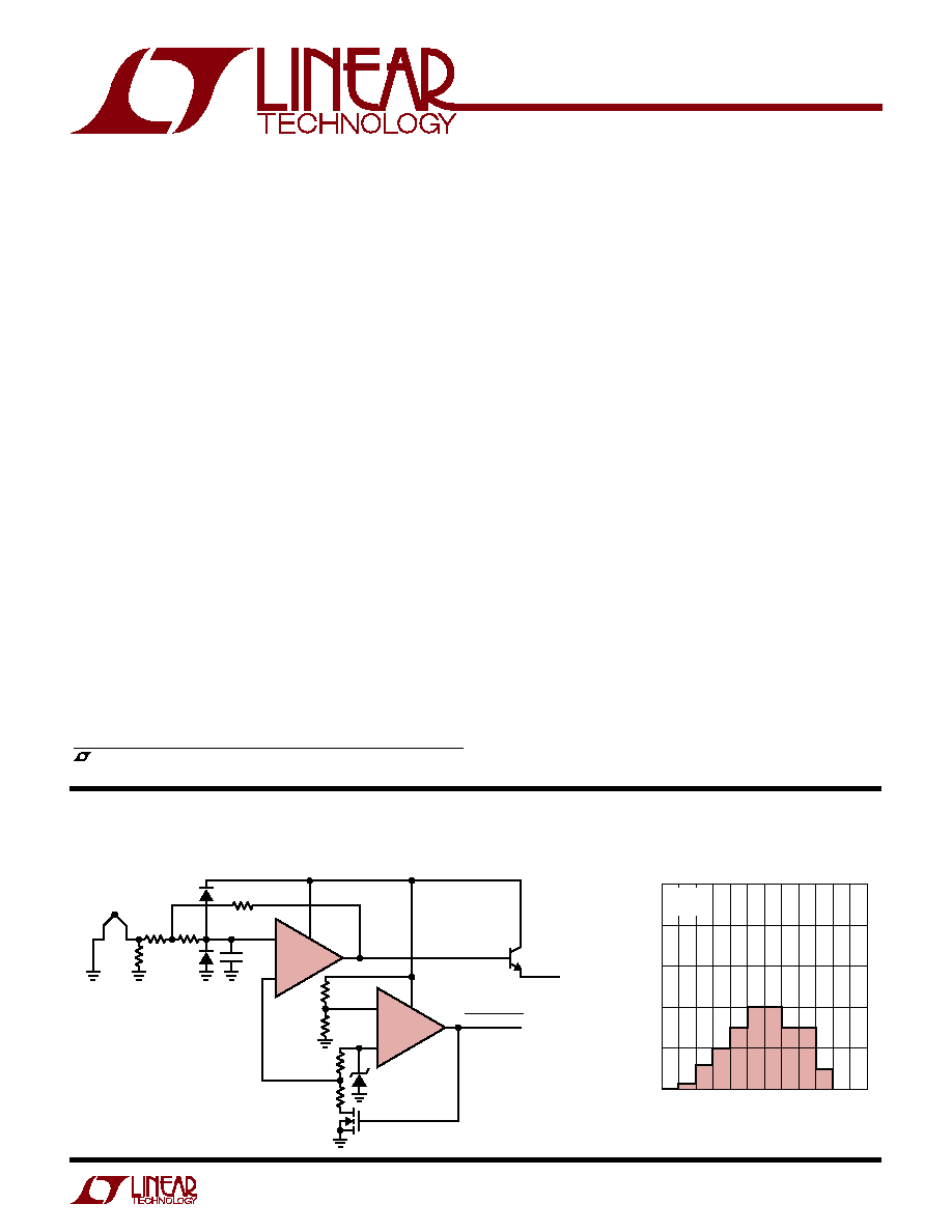
Total of 839 Units
INPUT OFFSET VOLTAGE (
µV)
≠600
PERCENT OF UNITS (%)
600
1541/42 TA02
≠300
0
300
50
40
30
20
10
0
V
CC
= 5V
V
SS
= 0V
≠
+
1
2
3
7
8
2N3904
SCR LOAD
5
2M
6
2.2
mF
1N457
LOW BATTERY
OUTPUT HIGH = "ON"
OUTPUT LOW = "OFF"
1.2V INTERNAL
REFERENCE
1541/42 ∑ TA01
≠
+
10k
VN2222
2M
1M
100k
10M
1k
≠
+
1/2 LTC1541
1/2 LTC1541
10k
I
CC
= 7
mA AT V
IN
= 5V
TYPE R
1N457
V
IN
= 3.6V TO 9V
Pilot Light Flame Detector with Low-Battery Lockout
FEATURES
DESCRIPTIO
U
APPLICATIO S
U
TYPICAL APPLICATIO
U
, LTC and LT are registered trademarks of Linear Technology Corporation.
2
LTC1541/LTC1542
15412fb
Supply Voltage ........................................................ 13V
Input Voltage .............................................≠ 0.3V to 13V
Output Voltage ...........................................≠ 0.3V to 13V
Output Short-Circuit Duration .......................... Indefinite
Storage Temperature Range ................. ≠ 65
C to 150C
(DD Package) ................................... ≠ 65
C to 125C
Operating Temperature Range (Note 7) .. ≠ 40
C to 85C
Specified Temperature Range (Note 8) ... ≠ 40
C to 85C
Lead Temperature (Soldering, 10 sec).................. 300
C
T
JMAX
= 150
C, q
JA
= 150
C/W
1
2
3
4
8
7
6
5
TOP VIEW
V
CC
COMPOUT
REF
COMPIN
+
AMPOUT
AMPIN
≠
AMPIN
+
V
SS
S8 PACKAGE
8-LEAD PLASTIC SO
1
2
3
4
AMPOUT
AMPIN
≠
AMPIN
+
V
SS
8
7
6
5
V
CC
COMPOUT
REF
COMPIN
+
TOP VIEW
MS8 PACKAGE
8-LEAD PLASTIC MSOP
T
JMAX
= 150
C, q
JA
= 250
C/W
T
JMAX
= 150
C, q
JA
= 150
C/W
1
2
3
4
8
7
6
5
TOP VIEW
V
CC
COMPOUT
COMPIN
≠
COMPIN
+
AMPOUT
AMPIN
≠
AMPIN
+
V
SS
S8 PACKAGE
8-LEAD PLASTIC SO
1
2
3
4
AMPOUT
AMPIN
≠
AMPIN
+
V
SS
8
7
6
5
V
CC
COMPOUT
COMPIN
≠
COMPIN
+
TOP VIEW
MS8 PACKAGE
8-LEAD PLASTIC MSOP
T
JMAX
= 150
C, q
JA
= 250
C/W
Consult LTC Marketing for parts specified with wider operating temperature ranges.
*Temperature grades are identified by a label on the shipping container.
ABSOLUTE AXI U RATI GS
W
W
W
U
(Note 1)
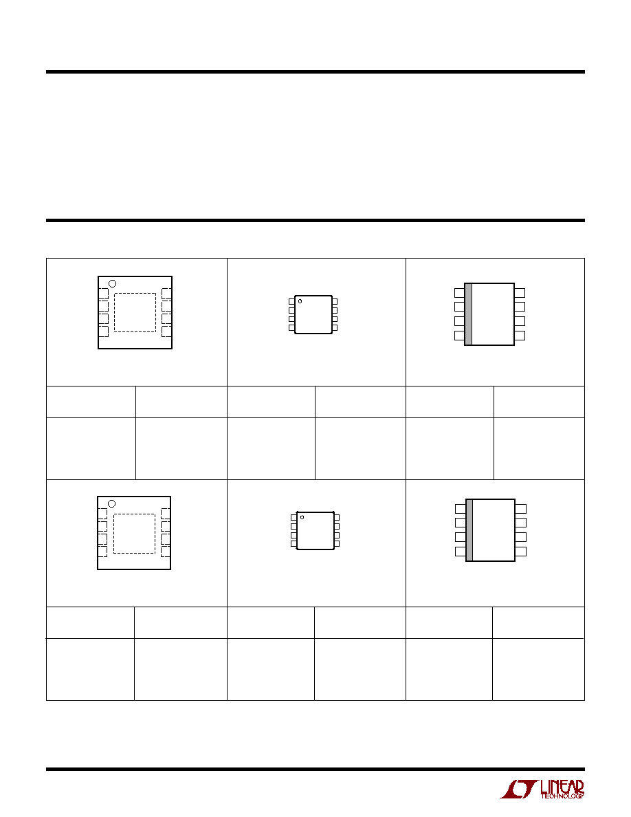
PACKAGE/ORDER I FOR ATIO
U
U
W
TOP VIEW
DD PACKAGE
8-LEAD (3mm 3mm) PLASTIC DFN
5
6
7
8
4
3
2
1
AMPOUT
AMPIN
≠
AMPIN
+
V
SS
V
CC
COMPOUT
REF
COMPIN
+
LTC1541CS8
LTC1541IS8
MS8
PART MARKING
ORDER PART
NUMBER
S8
PART MARKING
ORDER PART
NUMBER
1541
1541I
LTC1541CMS8
LTC1541IMS8
LTBE
LTADW
T
JMAX
= 125
C, q
JA
= 160
C/W (NOTE 6)
ORDER PART
NUMBER
LTC1541CDD
LTC1541IDD
DD
PART MARKING*
LAAT
LTC1542CS8
LTC1542IS8
1542
1542I
LTC1542CMS8
LTC1542IMS8
LTDE
LTADX
S8
PART MARKING
ORDER PART
NUMBER
MS8
PART MARKING
ORDER PART
NUMBER
ORDER PART
NUMBER
DD
PART MARKING*
TOP VIEW
DD PACKAGE
8-LEAD (3mm 3mm) PLASTIC DFN
5
6
7
8
4
3
2
1
AMPOUT
AMPIN
≠
AMPIN
+
V
SS
V
CC
COMPOUT
COMPIN
≠
COMPIN
+
T
JMAX
= 125
C, q
JA
= 160
C/W (NOTE 6)
LTC1542CDD
LTC1542IDD
LAAU
3
LTC1541/LTC1542
15412fb
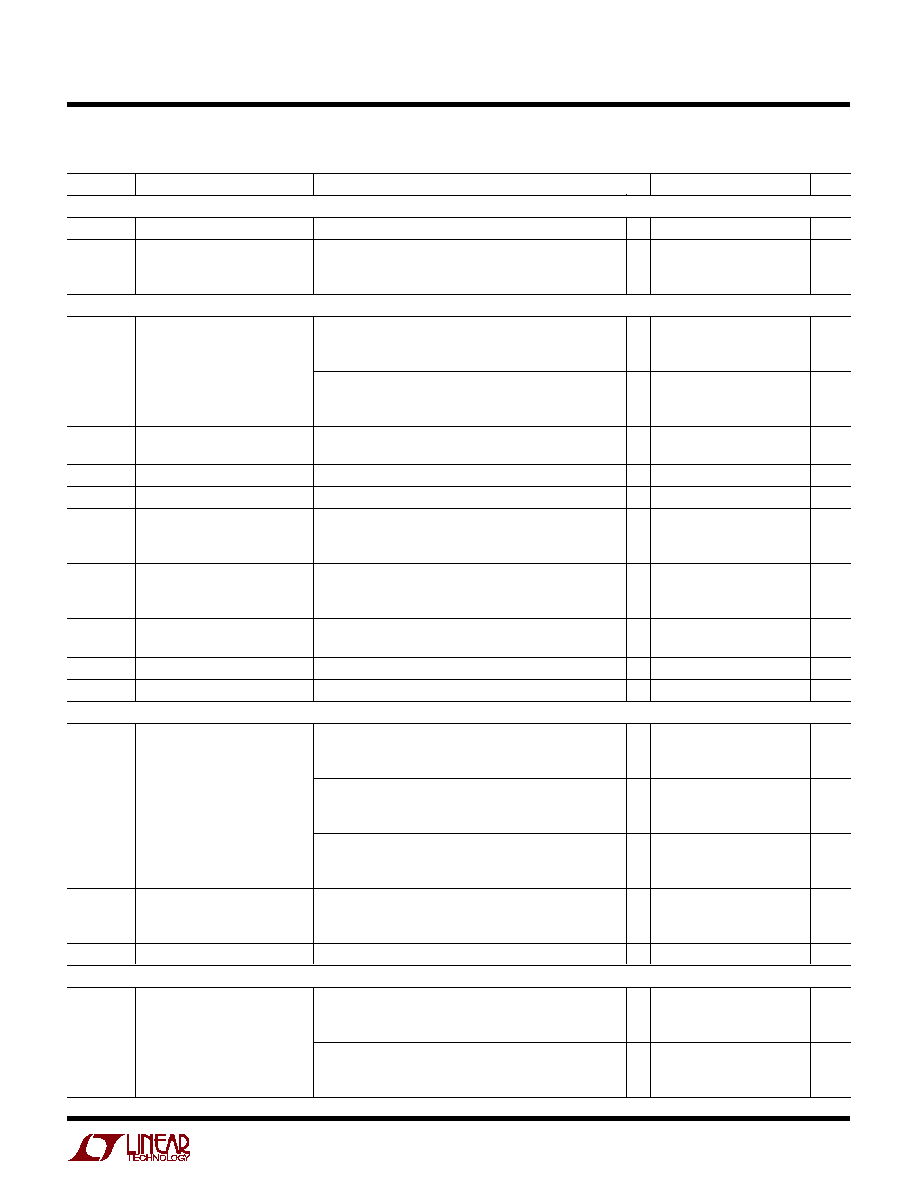
SYMBOL
PARAMETER
CONDITIONS
MIN
TYP
MAX
UNITS
The
denotes specifications which apply over the full operating
temperature range, otherwise specifications are at T
A
= 25
C. V
CC
= 5V, V
SS
= 0V, unless otherwise noted.
ELECTRICAL CHARACTERISTICS
Power Supply
V
CC
Supply Voltage Range
2.5
12.6
V
I
CC
Supply Current (Note 2)
5
10
mA
Commercial Grade
16
mA
Industrial Grade
17
mA
Comparator
V
OS
Input Offset Voltage (Note 3)
(SO-8)
1
mV
Commercial Grade (SO-8)
1.5
mV
Industrial Grade (SO-8)
2.0
mV
(MSOP)(DFN)
1.2
mV
Commercial Grade (MSOP)(DFN)
2.0
mV
Industrial Grade (MSOP)(DFN)
2.5
mV
V
TRIP
Trip Point (Note 4)
1.7
2.25
2.8
mV
1
3.8
mV
I
IN
Input Leakage Current (Note 5)
0.01
1
nA
V
CM
Input Common Mode Range
V
SS
V
CC
≠ 1.3V
V
CMRR
Common Mode Rejection Ratio
V
CM
= V
SS
to (V
CC
≠ 1.3V) (LTC1542)
0.7
mV/V
Commercial Grade
0.8
mV/V
Industrial Grade
0.9
mV/V
PSRR
Power Supply Rejection Ratio
V
CC
= 3V to 12V
0.25
mV/V
Commercial Grade (SO-8)
0.30
mV/V
Industrial Grade (SO-8)
0.35
mV/V
t
PD
Propagation Delay
Overdrive = 10mV
20
ms
Overdrive = 100mV
8
ms
V
OH
Output High Voltage
I
OUT
= ≠ 2mA
V
CC
≠ 0.2V
V
V
OL
Output Low Voltage
I
OUT
= 1.8mA
V
SS
+ 0.3V
V
Reference (LTC1541 Only)
V
REF
Reference Voltage
No Load (SO-8)
1.195
1.200
1.205
V
Commercial Grade (SO-8)
1.190
1.210
V
Industrial Grade (SO-8)
1.188
1.212
V
No Load (MSOP)
1.190
1.200
1.210
V
Commercial Grade (MSOP)
1.185
1.215
V
Industrial Grade (MSOP)
1.183
1.217
V
No Load (DFN)
1.185
1.200
1.215
V
Commercial Grade (DFN)
1.180
1.220
V
Industrial Grade (DFN)
1.178
1.222
V
DV
REF
Load Regulation
I
SOURCE
= 2mA
2
6
mV
I
SINK
= 10
mA
0.2
1.5
mV
5
mV
e
n
Voltage Noise
0.1Hz to 10Hz
16
mV
P-P
Op Amp
V
OS
Input Offset Voltage
V
CM
= 2.5V (SO-8)
0.7
mV
Commercial Grade (SO-8)
1.25
mV
Industrial Grade (SO-8)
1.65
mV
V
CM
= 2.5V (MSOP) (DFN)
1.00
mV
Commercial Grade (MSOP) (DFN)
1.75
mV
Industrial Grade (MSOP) (DFN)
2.0
mV
4
LTC1541/LTC1542
15412fb
I
B
Input Bias Current
V
CM
= 2.5V
0.01
1
nA
A
VOL
Large-Signal Gain
AMPOUT = 0.5V to 4.5V, No Load
80
1000
V/mV
AMPOUT = 0.5V to 4.5V, R
LOAD
= 100k
60
500
V/mV
Commercial Grade
38
V/mV
Industrial Grade
35
V/mV
GBW
Gain Bandwidth
A
V
= 1V/V
12
kHz
SR
Slew Rate
A
V
= 1V/V
8
V/ms
V
CM
Input Common Mode Range
V
SS
V
CC
≠ 1.3V
V
CMRR
Common Mode Rejection Ratio
V
CM
= V
SS
to (V
CC
≠ 1.3V)
0.5
mV/V
Commercial Grade
0.6
mV/V
Industrial Grade
0.6
mV/V
PSRR
Power Supply Rejection Ratio
V
CC
= 3V to 12V
0.19
mV/V
Commercial Grade
0.21
mV/V
Industrial Grade
0.23
mV/V
V
OH
Output High Voltage
R
LOAD
= 100k to V
SS
V
CC
≠ 0.07
V
Commercial Grade
V
CC
≠ 0.10
V
Industrial Grade
V
CC
≠ 0.12
V
V
OL
Output Low Voltage
R
LOAD
= 100k to V
CC
V
SS
+ 0.05
V
Commercial Grade
V
SS
+ 0.10
V
Industrial Grade
V
SS
+ 0.12
V
I
SOURCE
Output Source Current
0.9
1.8
mA
0.7
mA
I
SINK
Output Sink Current
1.3
1.8
mA
0.9
mA
e
n
Input Noise Voltage
f
O
= 0.1Hz to 10Hz
3
mV
P-P
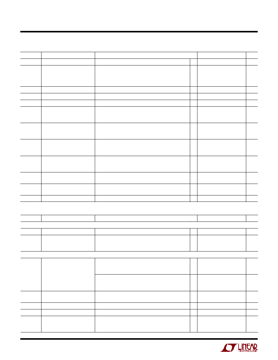
SYMBOL
PARAMETER
CONDITIONS
MIN
TYP
MAX
UNITS
The
denotes specifications which apply over the full operating
temperature range, otherwise specifications are at T
A
= 25
C. V
CC
= 5V, V
SS
= 0V, unless otherwise noted.
ELECTRICAL CHARACTERISTICS
The
denotes specifications which apply over the full operating temperature range, otherwise specifications are at T
A
= 25
C.
V
CC
= 3V, V
SS
= 0V, unless otherwise noted.
SYMBOL
PARAMETER
CONDITIONS
MIN
TYP
MAX
UNITS
Power Supply
V
CC
Supply Voltage Range
2.5
12.6
V
I
CC
Supply Current (Note 2)
4.5
9.5
mA
Commercial Grade
15
mA
Industrial Grade
16
mA
Comparator
V
OS
Input Offset Voltage (Note 3)
(SO-8)
1.0
mV
Commercial Grade (SO-8)
1.5
mV
Industrial Grade (SO-8)
2.0
mV
(MSOP)(DFN)
1.2
mV
Commercial Grade (MSOP)(DFN)
2.0
mV
Industrial Grade (MSOP)(DFN)
2.5
mV
V
TRIP
Trip Point (Note 4)
1.80
2.35
2.90
mV
1.00
3.90
mV
I
IN
Input Leakage Current (Note 5)
0.01
1
nA
V
CM
Input Common Mode Range
V
SS
V
CC
≠ 1.3
V
CMRR
Common Mode Rejection Ratio
V
CM
= V
SS
to (V
CC
≠ 1.3V) (LTC1542)
0.8
mV/V
Commercial Grade
0.9
mV/V
Industrial Grade
1.0
mV/V

5
LTC1541/LTC1542
15412fb
SYMBOL
PARAMETER
CONDITIONS
MIN
TYP
MAX
UNITS
The
denotes specifications which apply over the full operating
temperature range, otherwise specifications are at T
A
= 25
C. V
CC
= 3V, V
SS
= 0V, unless otherwise noted.
ELECTRICAL CHARACTERISTICS
PSRR
Power Supply Rejection Ratio
V
CC
= 3V to 12V
0.25
mV/V
Commercial Grade
0.30
mV/V
Industrial Grade
0.35
mV/V
t
PD
Propagation Delay
Overdrive = 10mV
25
ms
Overdrive = 100mV
12
ms
V
OH
Output High Voltage
I
OUT
= ≠ 2mA
V
CC
≠ 0.2
V
V
OL
Output Low Voltage
I
OUT
= 1.8mA
V
SS
+ 0.3
V
Reference (LTC1541 Only)
V
REF
Reference Voltage
No Load (SO-8)
1.195
1.200
1.205
V
Commercial Grade (SO-8)
1.190
1.210
V
Industrial Grade (SO-8)
1.188
1.212
V
No Load (MSOP)
1.190
1.200
1.210
V
Commercial Grade (MSOP)
1.185
1.215
V
Industrial Grade (MSOP)
1.183
1.217
V
No Load (DFN)
1.185
1.200
1.215
V
Commercial Grade (DFN)
1.180
1.220
V
Industrial Grade (DFN)
1.178
1.222
V
DV
REF
Load Regulation
I
SOURCE
= 1mA
2
6
mV
I
SINK
= 10
mA
0.2
1.5
mV
5
mV
e
n
Voltage Noise
0.1Hz to 10Hz
16
mV
P-P
Op Amp
V
OS
Input Offset Voltage
V
CM
= 1.5V (SO-8)
0.7
mV
Commercial Grade (SO-8)
1.25
mV
Industrial Grade (SO-8)
1.65
mV
V
CM
= 1.5V (MSOP)
1.00
mV
Commercial Grade (MSOP) (DFN)
1.75
mV
Industrial Grade (MSOP) (DFN)
2.0
mV
I
B
Input Bias Current
V
CM
= 1.5V
0.01
1
nA
A
VOL
Large-Signal Gain
AMPOUT = 0.5V to 2.5V, No Load
80.0
1000
V/mV
AMPOUT = 0.5V to 2.5V, R
LOAD
= 100k
45.5
500
V/mV
Commercial Grade
22.0
V/mV
Industrial Grade
20.0
V/mV
GBW
Gain Bandwidth
A
V
= 1V/V
12
kHz
SR
Slew Rate
A
V
= 1V/V
8
V/ms
V
CM
Input Common Mode Range
V
SS
V
CC
≠ 1.3
V
CMRR
Common Mode Rejection Ratio
V
CM
= V
SS
to (V
CC
≠ 1.3V)
0.7
mV/V
Commercial Grade
0.8
mV/V
Industrial Grade
0.8
mV/V
PSRR
Power Supply Rejection Ratio
V
CC
= 3V to 12V
0.19
mV/V
Commercial Grade
0.21
mV/V
Industrial Grade
0.23
mV/V
V
OH
Output High Voltage
R
LOAD
= 100k to V
SS
V
CC
≠ 0.07
V
Commercial Grade
V
CC
≠ 0.10
V
Industrial Grade
V
CC
≠ 0.12
V
V
OL
Output Low Voltage
R
LOAD
= 100k to V
CC
V
CC
+ 0.05
V
Commercial Grade
V
CC
+ 0.10
V
Industrial Grade
V
CC
+ 0.12
V
6
LTC1541/LTC1542
15412fb
SYMBOL
PARAMETER
CONDITIONS
MIN
TYP
MAX
UNITS
I
SOURCE
Output Source Current
0.6
0.95
mA
0.4
mA
I
SINK
Output Sink Current
1.2
1.8
mA
0.8
mA
e
n
Input Noise Voltage
f
O
= 0.1Hz to 10Hz
3
mV
P-P
The
denotes specifications which apply over the full operating
temperature range, otherwise specifications are at T
A
= 25
C. V
CC
= 3V, V
SS
= 0V, unless otherwise noted.
ELECTRICAL CHARACTERISTICS
TYPICAL PERFOR A CE CHARACTERISTICS
U
W
SUPPLY VOLTAGE (V)
2
3
4
5
6
7
8
9
10 11 12
SUPPLY CURRENT (
µ
A)
1541/42 TPC01
10
9
8
7
6
5
4
3
2
1
0
NONINVERTING
V
SS
= GND
AMPIN
+
= V
CC
/2
TEMPERATURE (
∞C)
≠50
≠25
0
25
50
75
100
125
SUPPLY CURRENT (
m
A)
1541/42 TPC02
10
9
8
7
6
5
4
3
2
V
CC
= 5V
V
SS
= GND
AMPIN
≠
= AMPOUT
AMPIN
+
= 2.5V
LOAD CURRENT (
µA)
REFERENCE OUTPUT VOLTAGE (V)
1.205
1.204
1.203
1.202
1.201
1.200
1.199
1.198
1.197
1.196
1.195
1
100
1000
10000
1541/42 TPC03
10
V
CC
= 5V
V
SS
= GND
SOURCING
CURRENT
SINKING
CURRENT
Supply Current vs Temperature
Reference Output Voltage vs
Load Current
Supply Current vs Supply Voltage
Note 6: The q
JA
specified for the DD package is with minimal PCB heat
spreading metal. Using expanded metal area on all layers of a board
reduces this value.
Note 7: The LTC1541C/LTC1541I and LTC1542C/LTC1542I are
guaranteed functional over the operating temperature range of ≠40
C to
85
C.
Note 8: The LTC1541C and LTC1542C are guaranteed to meet specified
performance from 0
C to 70C. The LTC1541C and LTC1542C are
designed, characterized and expected to meet performance from ≠40
C to
85
C, but are not tested or QA sampled at these temperatures. The
LTC1541I and LTC1542I are guaranteed to meet specified performance
from ≠40
C to 85C.
Note 1: Absolute Maximum Ratings are those values beyond which the life
of the device may be impaired.
Note 2: Supply current is tested with COMPIN
+
= (REF ≠ 100mV) for
LTC1541 and COMPIN
+
= 0V, COMPIN
≠
= 100mV for LTC1542.
Note 3: Input offset voltage is defined as the center of the input referred
hysteresis, V
CM
= REF (LTC1541). V
CM
= 1/2 V
CC
(LTC1542).
Note 4: Trip point is defined as the differential input voltage required to
make the comparator output change state. The difference between upper
and lower trip point is equal to the width of the input referred hysteresis,
V
CM
= REF (LTC1541). V
CM
= 1/2 V
CC
(LTC1542).
Note 5: The input leakage current is measured for COMPIN
+
at 0V
(LTC1541) and COMPIN
+
= COMPIN
≠
= 0V (LTC1542).
7
LTC1541/LTC1542
15412fb
TYPICAL PERFOR A CE CHARACTERISTICS
U
W
Comparator Short-Circuit Current
vs Supply Voltage
Op Amp Small-Signal Transient
Response
SUPPLY VOLTAGE (V)
2
3
4
5
6
7
8
9
10 11 12
SHORT-CIRCUIT CURRENT (mA)
1541/42 TPC10
250
200
150
100
50
0
≠50
≠100
≠150
≠200
≠250
SHORT TO V
SS
SHORT TO V
CC
NONINVERTING
1541/42 TPC11
A
VCL
= 1V/V
LOAD = 100k
W//100pF TO V
SS
V
SUPPLY
= 5V
INPUT
200mV/DIV
OUTPUT
100mV/DIV
Op Amp Large-Signal Transient
Response
NONINVERTING
1541/42 TPC11
A
VCL
= 1V/V
LOAD = 100k
W//100pF TO V
SS
V
SUPPLY
= 5V
INPUT
2V/DIV
OUTPUT
1V/DIV
SUPPLY VOLTAGE (V)
2
3
4
5
6
7
8
9
10 11 12
OUTPUT CURRENT (mA)
1541/42 TPC07
10
8
6
4
2
0
≠2
≠4
≠6
≠8
≠10
NONINVERTING
V
SS
= GND
AMPIN
+
= V
CC
/2
SHORT TO V
SS
SHORT TO V
CC
2
3
4
5
6
7
8
9
10 11 12
SUPPLY VOLTAGE (V)
DC OPEN-LOOP GAIN (V/mV)
10,000
1000
100
10
1
0.1
1541/42 TPC08
R
LOAD
= 100k
LOAD CURRENT (mA)
OUTPUT VOLTAGE (V)
5
4
3
2
1
0
0.01
1
10
1000
1541/42 TPC09
0.1
100
V
CC
= 5V
V
SS
= GND
SOURCING
CURRENT
SINKING
CURRENT
Op Amp Short-Circuit Current vs
Supply Voltage
Op Amp DC Open-Loop Gain vs
Supply Voltage
Comparator Output Voltage vs
Load Current
Op Amp Output Voltage vs
Load Current
LOAD CURRENT (
µA)
OUTPUT VOLTAGE (mV)
1
0.8
0.6
0.4
0.2
0
≠0.2
≠0.4
≠0.6
≠0.8
≠1
1
100
1000
10000
1541/42 TPC06
10
V
SUPPLY
=
±1.5V
V
SUPPLY
=
±1.5V
V
SUPPLY
=
±2.5V
V
SUPPLY
=
±2.5V
SOURCING
CURRENT
SINKING
CURRENT
≠50
≠25
0
25
50
75
100
125
TEMPERATURE (
∞C)
DC OPEN-LOOP GAIN (V/V)
1x10
6
1x10
5
1x10
4
1x10
3
1x10
2
1x10
1
1541/42 TPC05
V
CC
= 5V
V
SS
= GND
R
LOAD
= 100k
TEMPERATURE (
∞C)
≠50
≠25
0
25
50
75
100
125
REFERENCE OUTPUT (V)
1541/42 TPC04
1.202
1.201
1.200
1.199
1.198
1.197
1.196
1.195
V
CC
= 5V
V
SS
= GND
Reference Output Voltage vs
Temperature
Op Amp DC Open-Loop Gain vs
Temperature
8
LTC1541/LTC1542
15412fb
AMPOUT (Pin 1): Op Amp Output. The output can swing
from rail-to-rail while driving a capacitive load of up to
1000pF. The output can source and sink 0.7mA (min).
AMPIN
≠
(Pin 2): Inverting Input of Op Amp. The input
common mode ranges from V
SS
to (V
CC
≠ 1.3V). The input
current is typically 10pA at 25
C.
AMPIN
+
(Pin 3): Noninverting Input of Op Amp. The input
common mode ranges from V
SS
to (V
CC
≠ 1.3V). The input
current is typically 10pA at 25
C.
V
SS
(Pin 4): Negative Supply or Ground Connection.
COMPIN
+
(Pin 5): Noninverting Input of Comparator. The
input common mode ranges from V
SS
to (V
CC
≠ 1.3V). The
input current is typically 10pA at 25
C.
+
≠
7
8
6
5
1
2
3
4
LTC1542
LTC1542 ∑ BD
≠
+
COMPIN
+
COMPIN
≠
COMPOUT
V
CC
COMP
OP AMP
AMPOUT
AMPIN
≠
AMPIN
+
V
SS
+
≠
7
8
5
1
2
3
4
LTC1541
LTC1541 ∑ BD
≠
+
COMPIN
+
6
REF
COMPOUT
V
CC
COMP
OP AMP
AMPOUT
AMPIN
≠
AMPIN
+
V
SS
•1
U
U
U
PI FU CTIO S
BLOCK DIAGRA S
W
Op Amp Open-Loop Gain and
Phase vs Frequency
FREQUENCY (Hz)
OPEN-LOOP GAIN (dB)
PHASE SHIFT (DEGREES)
120
100
80
60
40
20
0
≠20
≠40
0
≠45
≠90
≠135
≠180
≠225
≠270
≠315
≠360
10
1k
10k
1M
1541/42 TPC13
100
100k
V
CC
= 5V
V
SS
= GND
R
LOAD
= 100k
PHASE
GAIN
REF (Pin 6) (LTC1541): Reference Output. V
REF
= 1.2V
±1% over industrial temperature range, and is also con-
nected to inverting comparator input internally. This de-
vice can source up to 2mA and sink up to 20
mA. The output
can drive a bypass capacitor of up to 0.01
mF without
oscillation.
COMPIN
≠
(Pin 6) (LTC1542): Inverting Input of Compara-
tor. The input common mode ranges from V
SS
to
(V
CC
≠ 1.3V). The input current is typically 10pA at 25
C.
COMPOUT (Pin 7): Comparator Output. The output can
source 20mA and sink 5mA.
V
CC
(Pin 8): Positive Supply, 2.5V
£ V
CC
£ 12.6V. The supply
bypass capacitors are not required if the supply impedance
is low. For single supply applications, it is a good general
practice to bypass V
CC
with a 0.1
mF capacitor to ground.
TYPICAL PERFOR A CE CHARACTERISTICS
U
W
9
LTC1541/LTC1542
15412fb
The LTC1541/LTC1542 are a combination of a micropower
op amp, comparator and 1.2V
±1% reference (LTC1541)
in an 8-pin package. The LTC1541 has the negative input
of the comparator internally connected to the reference
output. The supply voltage range is from 2.5V to 12.6V for
single supply and
±1.25V to ±6.3V for dual supplies. The
supply current is a mere 5
mA (typical) with a 5V single
supply.
Op Amp
The op amp is internally compensated to be unity-gain
stable, with typical GBW at 12kHz and slew rate of 8V/ms.
The output can drive a capacitive load of up to 1000pF and
swings from rail-to-rail. The input range is from the
negative rail to within 1.3V of the positive rail. The input
bias current is less than 1nA maximum at the extended
temperature range.
The output can source up to 2mA and sink up to 20
mA with
a 5V supply. The output can drive a bypass capacitor of up
to 0.01
mF without oscillation and by inserting a series
resistor, capacitance values up to 100
mF can be used
(Figure 1). Figure 2 shows the resistor value required for
different capacitor values to achieve critical damping.
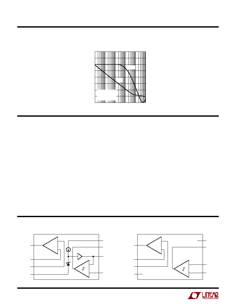
Bypassing the reference can help prevent false tripping of
the comparator by preventing glitches on V
CC
or reference
load transients from disturbing the reference output volt-
age. Figures 3a and 3b show the bypass reference output
with a square wave applied to the V
CC
pin while resistor R1
damps the reference response. Note that the comparator
output doesn't trip.
Op Amp Stability
Unlike other industry standard micropower CMOS op
amps, the op amp in the LTC1541/LTC1542 maintain
stability in unity-gain configuration while driving heavy
capacitive loads of up to 1000pF.
Although this family is primarily designed for low frequency
applications, good layout is extremely important. Low power,
high impedance circuits may increase the effects of board
leakage and stray capacitance. For example, the combina-
tion of a 10M resistance (from leakage between traces on a
contaminated, poorly designed PC board) and a 1pF stray
capacitance provides a pole at approximately 16kHz, which
is near the amplifier's bandwidth. Board routing and layout
should minimize leakage and stray capacitance. In some
cases, stray capacitance may be unavoidable and it may be
necessary to add a small capacitor across the feedback
resistor to compensate (Figure 4); select the smallest
capacitor value that ensures stability.
Inputs
The input common mode range for both the op amp and
comparator is from the negative supply to within 1.3V of the
positive supply. The inputs can be taken more than 300mV
below the negative supply without damaging the device if
the current out of the pin is limited to less than 1mA. Unlike
bipolar input op amps and comparators, the outputs of the
CMOS LTC1541/LTC1542 will not reverse phase when the
inputs are taken above the common mode input range.
Figure 1. Damping the Reference Output
8
4
LTC1541
1541/42 ∑ F01
6
REF
V
CC
GND
R1
C1
1
Comparator
The comparator has a high impedance differential input
stage with a common mode input range from the negative
rail to within 1.3V of the positive rail. The CMOS output
stage can swing from rail-to-rail and source up to 20mA
continuously. The output stage has been designed to
eliminate the power supply glitches that normally occur
when the output changes logic state. In addition, internal
hysteresis (
±3mV) ensures clean output switching even
with slow moving input signals. The negative input is
internally connected to the reference for the LTC1541.
Reference
The internal bandgap reference has an output voltage of
1.2V
±1% over the industrial grade temperature range.
APPLICATIO S I FOR ATIO
W
U
U
U
10
LTC1541/LTC1542
15412fb
CAPACITOR VALUE (
µF)
0.001
0.1
RESISTOR VALUE (k
)
10
1000
0.01
0.1
10
1
1541/42 ∑ F02
1
100
Figure 2. Damping Resistance vs Bypass Capacitor Value
8
7
4
LTC1541
1541/42 ∑ F03a
6 REF
5
COMPIN
+
COMPOUT
V
CC
GND
R1
430
C1
1
µF
1
+
≠
5V TO 8V
COMP
Figure 3a. Reference Transient Response Test Circuit
7.5
10W
DALE
HLM-10
12V
5AHR
GEL CELL
4
8
+
≠
1
1/2
LTC1541
3
2
7
5
6
1541/42 TA06
+
≠
1/2
LTC1541
1M
VN2222
Si9405
1M
3.65M
1A
SOLAR
ARRAY
6.8V
ZENER
1N754
340k
TIP121
8M
2A
FUSE
1M
V
REF
= 1.2V
(INTERNAL)
LOAD
Shunt Battery Charger with Low-Battery Load Disconnect
1541/42 ∑ F04
R2
2pF TO 10pF
≠
+
OP AMP
AMPIN
+
AMPOUT
R1
Figure 4. Compensation for Feedback Node Capacitance
8V
5V
V
REF
OUT
V
+
2mV/DIV
2ms/DIV
LTC1541 ∑ F03b
Figure 3b. Reference and Comparator Output Transient Response
APPLICATIO S I FOR ATIO
W
U
U
U
TYPICAL APPLICATIO S
U
11
LTC1541/LTC1542
15412fb
Information furnished by Linear Technology Corporation is believed to be accurate and reliable.
However, no responsibility is assumed for its use. Linear Technology Corporation makes no represen-
tation that the interconnection of its circuits as described herein will not infringe on existing patent rights.
U
PACKAGE DESCRIPTIO
3.00
±0.10
(4 SIDES)
NOTE:
1. DRAWING TO BE MADE A JEDEC PACKAGE OUTLINE M0-229 VARIATION OF (WEED-1)
2. ALL DIMENSIONS ARE IN MILLIMETERS
3. DIMENSIONS OF EXPOSED PAD ON BOTTOM OF PACKAGE DO NOT INCLUDE
MOLD FLASH. MOLD FLASH, IF PRESENT, SHALL NOT EXCEED 0.15mm ON ANY SIDE
4. EXPOSED PAD SHALL BE SOLDER PLATED
0.38
± 0.10
BOTTOM VIEW--EXPOSED PAD
1.65
± 0.10
(2 SIDES)
0.75
±0.05
R = 0.115
TYP
2.38
±0.10
(2 SIDES)
1
4
8
5
PIN 1
TOP MARK
0.200 REF
0.00 ≠ 0.05
(DD8) DFN 0203
0.28
± 0.05
2.38
±0.05
(2 SIDES)
RECOMMENDED SOLDER PAD PITCH AND DIMENSIONS
1.65
±0.05
(2 SIDES)
2.15
±0.05
0.50
BSC
0.675
±0.05
3.5
±0.05
PACKAGE
OUTLINE
0.28
± 0.05
0.50 BSC
MSOP (MS8) 0802
0.53
± 0.015
(.021
± .006)
SEATING
PLANE
NOTE:
1. DIMENSIONS IN MILLIMETER/(INCH)
2. DRAWING NOT TO SCALE
3. DIMENSION DOES NOT INCLUDE MOLD FLASH, PROTRUSIONS OR GATE BURRS.
MOLD FLASH, PROTRUSIONS OR GATE BURRS SHALL NOT EXCEED 0.152mm (.006") PER SIDE
4. DIMENSION DOES NOT INCLUDE INTERLEAD FLASH OR PROTRUSIONS.
INTERLEAD FLASH OR PROTRUSIONS SHALL NOT EXCEED 0.152mm (.006") PER SIDE
5. LEAD COPLANARITY (BOTTOM OF LEADS AFTER FORMING) SHALL BE 0.102mm (.004") MAX
0.18
(.077)
0.254
(.010)
1.10
(.043)
MAX
0.22 ≠ 0.38
(.009 ≠ .015)
TYP
0.13
± 0.076
(.005
± .003)
0.86
(.034)
REF
0.65
(.0256)
BSC
0
∞ ≠ 6∞ TYP
DETAIL "A"
DETAIL "A"
GAUGE PLANE
1
2
3
4
4.90
± 0.15
(1.93
± .006)
8
7 6 5
3.00
± 0.102
(.118
± .004)
(NOTE 3)
3.00
± 0.102
(.118
± .004)
NOTE 4
0.52
(.206)
REF
5.23
(.206)
MIN
3.2 ≠ 3.45
(.126 ≠ .136)
0.889
± 0.127
(.035
± .005)
RECOMMENDED SOLDER PAD LAYOUT
0.42
± 0.04
(.0165
± .0015)
TYP
0.65
(.0256)
BSC
DD Package
8-Lead Plastic DFN (3mm
• 3mm)
(Reference LTC DWG # 05-08-1698)
MS8 Package
8-Lead Plastic MSOP
(Reference LTC DWG # 05-08-1660)
S8 Package
8-Lead Plastic Small Outline (Narrow .150 Inch)
(Reference LTC DWG # 05-08-1610)
.016 ≠ .050
(0.406 ≠ 1.270)
.010 ≠ .020
(0.254 ≠ 0.508)
45
∞
0
∞≠ 8∞ TYP
.008 ≠ .010
(0.203 ≠ 0.254)
SO8 0303
.053 ≠ .069
(1.346 ≠ 1.752)
.014 ≠ .019
(0.355 ≠ 0.483)
TYP
.004 ≠ .010
(0.101 ≠ 0.254)
.050
(1.270)
BSC
1
2
3
4
.150 ≠ .157
(3.810 ≠ 3.988)
NOTE 3
8
7
6
5
.189 ≠ .197
(4.801 ≠ 5.004)
NOTE 3
.228 ≠ .244
(5.791 ≠ 6.197)
.245
MIN
.160
±.005
RECOMMENDED SOLDER PAD LAYOUT
.045
±.005
.050 BSC
.030
±.005
TYP
INCHES
(MILLIMETERS)
NOTE:
1. DIMENSIONS IN
2. DRAWING NOT TO SCALE
3. THESE DIMENSIONS DO NOT INCLUDE MOLD FLASH OR PROTRUSIONS.
MOLD FLASH OR PROTRUSIONS SHALL NOT EXCEED .006" (0.15mm)
12
LTC1541/LTC1542
15412fb
,, LINEAR TECHNOLOGY CORPORATION 1998
LT/TP 0503 1K REV B ∑ PRINTED IN USA
PART NUMBER
DESCRIPTION
COMMENTS
LT
Æ
1078/LT1079
Dual/Quad Micropower, Single Supply Precision Op Amps
70
mV, V
OS
Max and 0.4
mV/C Drift, 200kHz GBW, 0.07V/ms
Slew Rate, Input/Output Common Mode Includes Ground
LT1178/LT1179
Dual/Quad 17
mA Max, Single Supply Precision Op Amps
70
mV, V
OS
Max and 2.5
mV/C Drift Max, 85kHz GBW, 0.04V/ms
Slew Rate, Input/Output Common Mode Includes Ground
LT1490/LT1491
Dual/Quad Micropower Rail-to-Rail Input and Output Op Amps Single Supply Input Range: ≠ 0.4V to 44V, Micropower 50
mA
Amplifier, Rail-to-Rail Input and Output, 200kHz GBW
LT1635
Micropower Rail-to-Rail Op Amp and Reference
130
mA of Supply Current, 1.3mV V
OS
Max
LT2078/LT2079
Dual/Quad Micropower, Single Supply Precision Op Amps
SO-8 and 14-Lead Standard Pinout, 70
mV V
OS
Max, 200kHz GBW
LT2178/LT2179
Dual/Quad 17
mA Max, Single Supply Precision Op Amps
SO-8 and 14-Lead Standard Pinout, 70
mV V
OS
Max, 85kHz GBW
RELATED PARTS
TYPICAL APPLICATIO S
U
R1
220
0.25W
V
CC
+
≠
+
≠
2
1
3
6
7
8
5
4
R1
1M
Q2
2N3906
Q1
FZT2907A
V
IN
6V
300mA
SHUTDOWN
IC1
LTC1541
V
SS
1541/42 TA07
R4
100k
1%
R3
3.83k
1%
R7
0.15
R5
2.2M
R8
249k
0.5%
300mA
4.2V FLOAT
Li-ION
C3
0.01
µF
C1
4700pF
D1
1N5817
C2
0.1
µF
R6
33k
R9
100k
0.5%
1
Linear Lithium-Ion Charger
Voltage Control Oscillator
≠
+
1
4
8
LTC1542
OP AMP
2
3
7
6
5
5V
0V
V
OUT
V
CC
V
IN
0V ≠ V
CC
1541/42 TA03
≠
+
R4
5M
1M
1M
R2
150k
R1
300k
R4
1.1M
VN2222
VN2222
C1
0.047
µF
R3
500k
FREQ
V
C
2.4C ∑ R1 ∑ V
CC
VALUES SHOWN ARE FOR
100Hz WITH V
IN
= V
CC
LTC1542
COMP
Linear Technology Corporation
1630 McCarthy Blvd., Milpitas, CA 95035-7417
(408) 432-1900
FAX: (408) 434-0507
www.linear.com
≠
+
1
4
8
2
3
7
5
6
1541/42 TA04
≠
+
LTC1542
OP AMP
LTC1542
COMP
5M
5M
0.1
µF
R2
500k
R1
10M
R3
5M
FREQ
R1
4C ∑ R2 ∑ R3
V
CC
3V TO 12V
Single Supply Function Generator
1541/42 TA05
+
≠
LTC1542
OP AMP
V
SS
≠3V
V
CC
3V TO 9V
V
OUT
≠2.5V
1
4
8
2
3
200k
LT1634-2.5
Negative Reference