 | –≠–ª–µ–∫—Ç—Ä–æ–Ω–Ω—ã–π –∫–æ–º–ø–æ–Ω–µ–Ω—Ç: LTC1544I | –°–∫–∞—á–∞—Ç—å:  PDF PDF  ZIP ZIP |
1
LTC1544
Software-Selectable
Multiprotocol Transceiver
D2
D1
LTC1544
RTS
DTR
DSR
DCD
CTS
D3
R2
R1
R4
R3
D2
LTC1543
LL
TXD
SCTE
TXC
RXC
RXD
2
14
24
11
15
12
17
9
3
1
4
19
20
6
23
22
5
13
8
10
18
7
16
1544 TA01
LTC1344A
D3
R2
R1
R3
D1
TXD A (103)
TXD B
SCTE A (113)
SCTE B
RXC A (115)
RXC B
RXD A (104)
RXD B
RTS A (105)
RTS B
DTR A (108)
DTR B
CTS A (106)
CTS B
LL A (141)
SG (102)
SHIELD (101)
DB-25 CONNECTOR
TXC A (114)
TXC B
DCD A (107)
DCD B
DSR A (109)
DSR B
D4
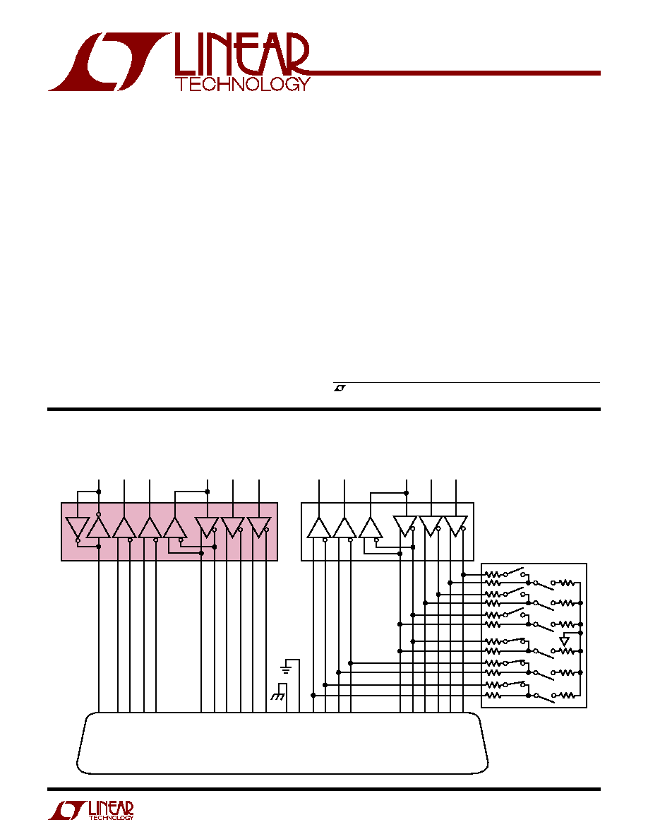
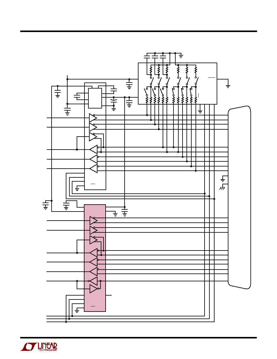
DTE or DCE Multiprotocol Serial Interface with DB-25 Connector
, LTC and LT are registered trademarks of Linear Technology Corporation.
s
Data Networking
s
CSU and DSU
s
Data Routers
s
Software-Selectable Transceiver Supports:
RS232, RS449, EIA530, EIA530-A, V.35, V.36, X.21
s
TUV/Detecon Inc. Certified NET1 and NET2
Compliant (Test Report No. NET2/102201/97)
s
TBR2 Compliant (Test Report No. CTR2/022701/98)
s
Software-Selectable Cable Termination Using
the LTC1344A
s
Complete DTE or DCE Port with LTC1543, LTC1344A
or LTC1546 with Integrated Termination
s
Operates from Single 5V Supply with LTC1543
The LTC
Æ
1544 is a 4-driver/4-receiver multiprotocol trans-
ceiver. The LTC1544 and LTC1543 form the core of a
complete software-selectable DTE or DCE interface port that
supports the RS232, RS449, EIA530, EIA530-A, V.35, V.36
or X.21 protocols. Cable termination for the LTC1543 may be
implemented using the LTC1344A software-selectable cable
termination chip or by using existing discrete designs. The
LTC1546 includes software-selectable cable termination on-
chip.
The LTC1544 runs from a 5V supply and the charge pump on
the LTC1543 or LTC1546. The part is available in a 28-lead
SSOP surface mount package.
FEATURES
DESCRIPTIO
U
APPLICATIO S
U
TYPICAL APPLICATIO
U
2
LTC1544
ORDER PART
NUMBER
(Note 1)
Supply Voltage, V
CC
................................................ 6.5V
Input Voltage
Transmitters ........................... ≠ 0.3V to (V
CC
+ 0.3V)
Receivers ............................................... ≠ 18V to 18V
Logic Pins .............................. ≠ 0.3V to (V
CC
+ 0.3V)
Output Voltage
Transmitters .................. (V
EE
≠ 0.3V) to (V
DD
+ 0.3V)
Receivers ................................ ≠ 0.3V to (V
CC
+ 0.3V)
V
EE
........................................................ ≠ 10V to 0.3V
V
DD
....................................................... ≠ 0.3V to 10V
Short-Circuit Duration
Transmitter Output ..................................... Indefinite
Receiver Output .......................................... Indefinite
V
EE
.................................................................. 30 sec
Operating Temperature Range
LTC1544CG ............................................. 0
∞
C to 70
∞
C
LTC1544IG ........................................ ≠ 40
∞
C to 85
∞
C
Storage Temperature Range ................ ≠ 65
∞
C to 150
∞
C
Lead Temperature (Soldering, 10 sec)................. 300
∞
C
LTC1544CG
LTC1544IG
T
JMAX
= 150
∞
C,
JA
= 65
∞
C/ W
1
2
3
4
5
6
7
8
9
10
11
12
13
14
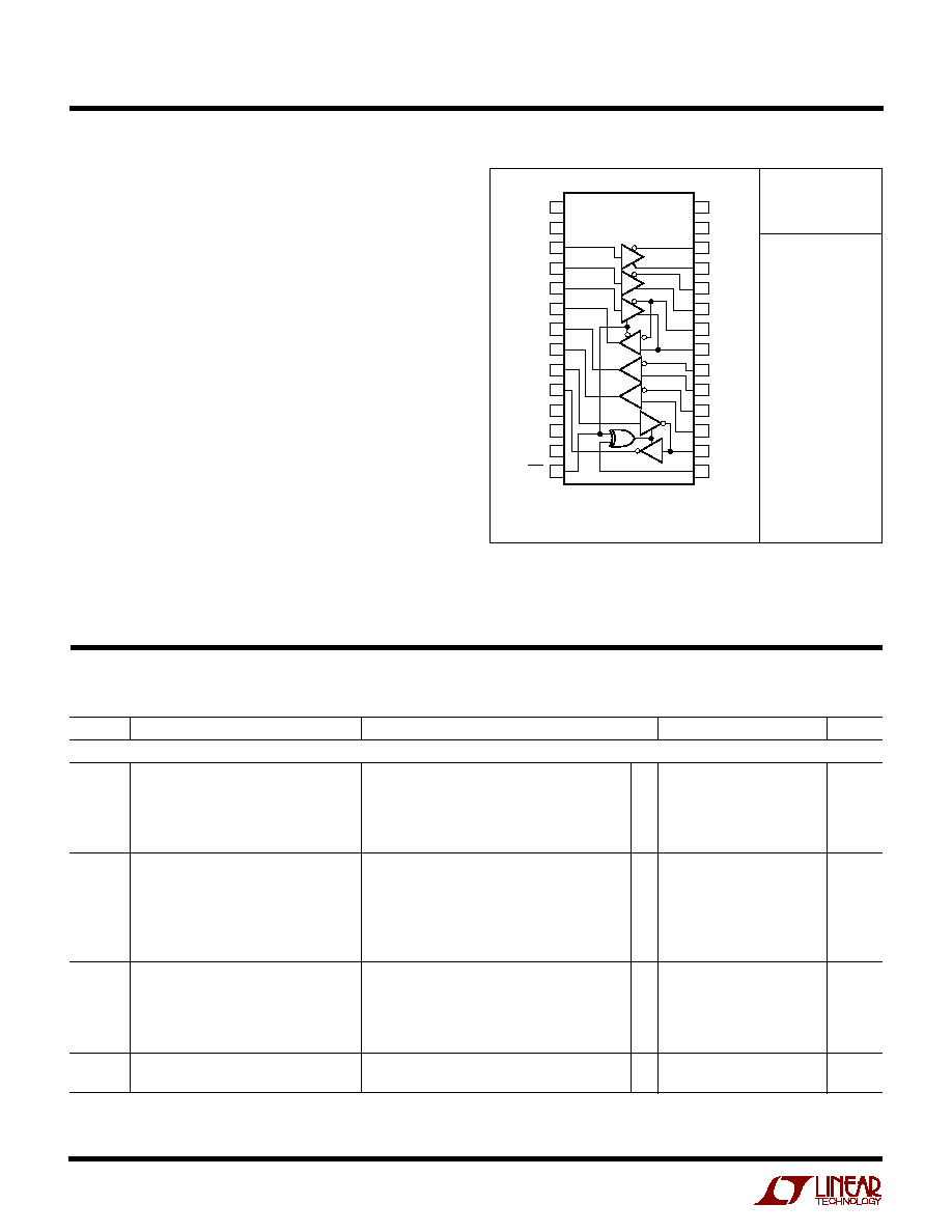
TOP VIEW
28
27
26
25
24
23
22
21
20
19
18
17
16
15
V
CC
V
DD
D1
D2
D3
R1
R2
R3
D4
R4
M0
M1
M2
DCE/DTE
V
EE
GND
D1 A
D1 B
D2 A
D2 B
D3/R1 A
D3/R1 B
R2 A
R2 B
R3 A
R3 B
D4/R4 A
INVERT
R1
D2
D1
R2
D3
G PACKAGE
28-LEAD PLASTIC SSOP
R3
D4
R4
Consult factory for Military grade parts.
The
q
denotes specifications which apply over the full operating tempera-
ture range, otherwise specifications are at T
A
= 25
∞
C. V
CC
= 5V, V
DD
= 8V, V
EE
= ≠ 7V for V.28, ≠ 5.5V for V.10, V.11 (Notes 2, 3)
SYMBOL
PARAMETER
CONDITIONS
MIN
TYP
MAX
UNITS
Supplies
I
CC
V
CC
Supply Current (DCE Mode,
RS530, RS530-A, X.21 Modes, No Load
2.7
mA
All Digital Pins = GND or V
CC
)
RS530, RS530-A, X.21 Modes, Full Load
q
95
120
mA
V.28 Mode, No Load
q
1
2
mA
V.28 Mode, Full Load
q
1
2
mA
No-Cable Mode
q
10
200
µ
A
I
EE
V
EE
Supply Current (DCE Mode,
RS530, RS530-A, X.21 Modes, No Load
2.1
mA
All Digital Pins = GND or V
CC
)
RS530, X.21 Modes, Full Load
14
mA
V
EE
= ≠ 5.6V (RS530, RS530-A Modes) RS530-A, Full Load
25
mA
V
EE
= ≠ 8.46V (V.28 Mode)
V.28 Mode, No Load
1
mA
V.28 Mode, Full Load
12
mA
No-Cable Mode
10
µ
A
I
DD
V
DD
Supply Current (DCE Mode,
RS530, RS530-A, X.21 Modes, NoLoad
0.2
mA
All Digital Pins = GND or V
CC
)
RS530, RS530-A, X.21 Modes, Full Load
0.2
mA
V
DD
= 8.73V
V.28 Mode, No Load
1
mA
V.28 Mode, Full Load
12
mA
No-Cable Mode
10
µ
A
P
D
Internal Power Dissipation (DCE Mode,
RS530, RS530-A, X.21 Modes, Full Load
300
mW
(All Digital Pins = GND or V
CC
)
V.28 Mode, Full Load
54
mW
ABSOLUTE AXI U RATI GS
W
W
W
U
PACKAGE/ORDER I FOR ATIO
U
U
W
ELECTRICAL CHARACTERISTICS
3
LTC1544
The
q
denotes specifications which apply over the full operating tempera-
ture range, otherwise specifications are at T
A
= 25
∞
C. V
CC
= 5V, V
DD
= 8V, V
EE
= ≠ 7V for V.28, ≠ 5.5V for V.10, V.11 (Notes 2, 3)
SYMBOL
PARAMETER
CONDITIONS
MIN
TYP
MAX
UNITS
Logic Inputs and Outputs
V
IH
Logic Input High Voltage
q
2
V
V
IL
Logic Input Low Voltage
q
0.8
V
I
IN
Logic Input Current
D1, D2, D3, D4
q
±
10
µ
A
M0, M1, M2, DCE, INVERT = GND (LTC1544C)
q
≠ 100
≠ 50
≠ 30
µ
A
M0, M1, M2, DCE, INVERT = GND (LTC1544I)
q
≠ 120
≠ 50
≠ 30
µ
A
M0, M1, M2, DCE, INVERT = V
CC
q
±
10
µ
A
V
OH
Output High Voltage
I
O
= ≠ 4mA
q
3
4.5
V
V
OL
Output Low Voltage
I
O
= 4mA
q
0.3
0.8
V
I
OSR
Output Short-Circuit Current
0V
V
O
V
CC
q
≠ 50
40
50
mA
I
OZR
Three-State Output Current
M0 = M1 = M2 = V
CC
, 0V
V
O
V
CC
±
1
µ
A
V.11 Driver
V
ODO
Open Circuit Differential Output Voltage
R
L
= 1.95k (Figure 1)
q
±
5
V
V
ODL
Loaded Differential Output Voltage
R
L
= 50
(Figure 1)
0.5V
ODO
0.67V
ODO
V
R
L
= 50
(Figure 1)
q
±
2
V
V
OD
Change in Magnitude of Differential
R
L
= 50
(Figure 1)
q
0.2
V
Output Voltage
V
OC
Common Mode Output Voltage
R
L
= 50
(Figure 1)
q
3
V
V
OC
Change in Magnitude of Common Mode
R
L
= 50
(Figure 1)
q
0.2
V
Output Voltage
I
SS
Short-Circuit Current
V
OUT
= GND
±
150
mA
I
OZ
Output Leakage Current
≠ 0.25V
V
O
0.25V, Power Off or
q
±
1
±
100
µ
A
No-Cable Mode or Driver Disabled
t
r
, t
f
Rise or Fall Time
LTC1544C (Figures 2, 5)
q
2
15
25
ns
LTC1544I (Figures 2, 5)
q
2
15
35
ns
t
PLH
Input to Output
LTC1544C (Figures 2, 5)
q
20
40
65
ns
LTC1544I (Figures 2, 5)
q
20
40
75
ns
t
PHL
Input to Output
LTC1544C (Figures 2, 5)
q
20
40
65
ns
LTC1544I (Figures 2, 5)
q
20
40
75
ns
t
Input to Output Difference,
t
PLH
≠ t
PHL
LTC1544C (Figures 2, 5)
q
0
3
12
ns
LTC1544I (Figures 2, 5)
q
0
3
17
ns
t
SKEW
Output to Output Skew
(Figures 2, 5)
3
ns
V.11 Receiver
V
TH
Input Threshold Voltage
≠ 7V
V
CM
7V
q
≠ 0.2
0.2
V
V
TH
Input Hysteresis
≠ 7V
V
CM
7V
q
15
40
mV
I
IN
Input Current (A, B)
≠ 10V
V
A,B
10V
q
±
0.66
mA
R
IN
Input Impedance
≠ 10V
V
A,B
10V
q
15
30
k
t
r
, t
f
Rise or Fall Time
(Figures 2, 6)
15
ns
t
PLH
Input to Output
LTC1544C (Figures 2, 6)
q
50
80
ns
LTC1544I (Figures 2, 6)
q
50
90
ns
t
PHL
Input to Output
LTC1544C (Figures 2, 6)
q
50
80
ns
LTC1544I (Figures 2, 6)
q
50
90
ns
t
Input to Output Difference,
t
PLH
≠ t
PHL
LTC1544C (Figures 2, 6)
q
0
4
16
ns
LTC1544I (Figures 2, 6)
q
0
4
21
ns
ELECTRICAL CHARACTERISTICS
4
LTC1544
Note 1: Absolute Maximum Ratings are those beyond which the safety of a
device may be impaired.
Note 2: All currents into device pins are positive; all currents out of device
are negative. All voltages are referenced to device ground unless otherwise
specified.
Note 3: All typicals are given for V
CC
= 5V, V
DD
= 8V, V
EE
= ≠ 7V for V.28,
≠ 5.5V for V.10, V.11 and T
A
= 25
∞
C.
SYMBOL
PARAMETER
CONDITIONS
MIN
TYP
MAX
UNITS
V.10 Driver
V
O
Output Voltage
Open Circuit, R
L
= 3.9k
q
±
4
±
6
V
V
T
Output Voltage
R
L
= 450
(Figure 3)
q
±
3.6
V
R
L
= 450
(Figure 3)
0.9V
O
I
SS
Short-Circuit Current
V
O
= GND
±
150
mA
I
OZ
Output Leakage Current
≠ 0.25V
V
O
0.25V, Power Off or
q
±
0.1
±
100
µ
A
No-Cable Mode or Driver Disabled
t
r
, t
f
Rise or Fall Time
R
L
= 450
, C
L
= 100pF (Figures 3, 7)
2
µ
s
t
PLH
Input to Output
R
L
= 450
, C
L
= 100pF (Figures 3, 7)
1
µ
s
t
PHL
Input to Output
R
L
= 450
, C
L
= 100pF (Figures 3, 7)
1
µ
s
V.10 Receiver
V
TH
Receiver Input Threshold Voltage
q
≠ 0.25
0.25
V
V
TH
Receiver Input Hysteresis
q
25
50
mV
I
IN
Receiver Input Current
≠ 10V
V
A
10V
q
±
0.66
mA
R
IN
Receiver Input Impedance
≠ 10V
V
A
10V
q
15
30
k
t
r
, t
f
Rise or Fall Time
(Figures 4, 8)
15
ns
t
PLH
Input to Output
(Figures 4, 8)
55
ns
t
PHL
Input to Output
(Figures 4, 8)
109
ns
t
Input to Output Difference,
t
PLH
≠ t
PHL
(Figures 4, 8)
60
ns
V.28 Driver
V
O
Output Voltage
Open Circuit
q
±
10
V
R
L
= 3k (Figure 3)
q
±
5
±
8.5
V
I
SS
Short-Circuit Current
V
O
= GND
q
±
150
mA
I
OZ
Output Leakage Current
≠ 0.25V
V
O
0.25V, Power Off or
q
±
1
±
100
µ
A
No-Cable Mode or Driver Disabled
SR
Slew Rate
R
L
= 3k, C
L
= 2500pF (Figures 3, 7)
q
4
30
V/
µ
s
t
PLH
Input to Output
R
L
= 3k, C
L
= 2500pF (Figures 3, 7)
q
1.3
2.5
µ
s
t
PHL
Input to Output
R
L
= 3k, C
L
= 2500pF (Figures 3, 7)
q
1.3
2.5
µ
s
V.28 Receiver
V
THL
Input Low Threshold Voltage
q
1.5
0.8
V
V
TLH
Input High Threshold Voltage
q
2
1.6
V
V
TH
Receiver Input Hysterisis
q
0
0.1
0.3
V
R
IN
Receiver Input Impedance
≠ 15V
V
A
15V
q
3
5
7
k
t
r
, t
f
Rise or Fall Time
(Figures 4, 8)
15
ns
t
PLH
Input to Output
(Figures 4, 8)
q
60
100
ns
t
PHL
Input to Output
(Figures 4, 8)
q
150
450
ns
The
q
denotes specifications which apply over the full operating tempera-
ture range, otherwise specifications are at T
A
= 25
∞
C. V
CC
= 5V, V
DD
= 8V, V
EE
= ≠ 7V for V.28, ≠ 5.5V for V.10, V.11 (Notes 2, 3)
ELECTRICAL CHARACTERISTICS

5
LTC1544
V
CC
(Pin 1): Positive Supply for the Transceivers. 4.75V
V
CC
5.25V. Connect a 1
µ
F capacitor to ground.
V
DD
(Pin 2): Positive Supply Voltage for V.28. Connect to
V
DD
Pin 3 on LTC1543 or 8V supply. Connect a 1
µ
F
capacitor to ground.
D1 (Pin 3): TTL Level Driver 1 Input.
D2 (Pin 4): TTL Level Driver 2 Input.
D3 (Pin 5): TTL Level Driver 3 Input.
R1 (Pin 6): CMOS Level Receiver 1 Output.
R2 (Pin 7): CMOS Level Receiver 2 Output.
R3 (Pin 8): CMOS Level Receiver 3 Output.
D4 (Pin 9): TTL Level Driver 4 Input.
R4 (Pin 10): CMOS Level Receiver 4 Output.
M0 (Pin 11): TTL Level Mode Select Input 0 with Pull-Up
to V
CC
.
M1 (Pin 12): TTL Level Mode Select Input 1 with Pull-Up
to V
CC
.
M2 (Pin 13): TTL Level Mode Select Input 2 with Pull-Up
to V
CC
.
DCE/DTE (Pin 14): TTL Level Mode Select Input with
Pull-Up to V
CC
.
INVERT (Pin 15): TTL Level Mode Select Input with Pull-
Up to V
CC
.
D4/R4 A (Pin 16): Receiver 4 Inverting Input and Driver 4
Output.
R3 B (Pin 17): Receiver 3 Noninverting Input.
R3 A (Pin 18): Receiver 3 Inverting Input.
R2 B (Pin 19): Receiver 2 Noninverting Input.
R2 A (Pin 20): Receiver 2 Inverting Input.
D3/R1 B (Pin 21): Receiver 1 Noninverting Input and
Driver 3 Noninverting Output.
D3/R1 A (Pin 22): Receiver 1 Inverting Input and Driver 3
Inverting Output.
D2 B (Pin 23): Driver 2 Noninverting Output.
D2 A (Pin 24): Driver 2 Inverting Output.
D1 B (Pin 25): Driver 1 Noninverting Output.
D1 A (Pin 26): Driver 1 Inverting Output.
GND (Pin 27): Ground.
V
EE
(Pin 28): Negative Supply Voltage. Connect to V
EE
Pin
26 on LTC1543 or to ≠ 8V supply. Connect a 1
µ
F capacitor
to ground.
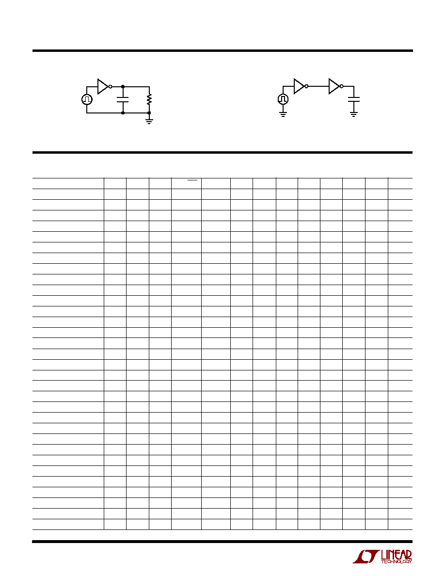
Figure 1. V.11 Driver Test Circuit
A
B
A
R
B
1544 F02
R
L
100
C
L
100pF
C
L
100pF
15pF
A
B
1544 F01
V
OD
V
OC
R
L
50
R
L
50
Figure 2. V.11 Driver/Receiver AC Test Circuit
U
U
U
PI FU CTIO S
TEST CIRCUITS
6
LTC1544
Figure 3. V.10/V.28 Driver Test Circuit
Figure 4. V.10/V.28 Receiver Test Circuit
A
D
1544 F04
15pF
R
A
A
D
1544 F03
R
L
C
L
LTC1544 MODE NAME
M2
M1
M0
DCE/DTE
INVERT
D1
D2
D3
R1
R2
R3
D4
R4
Not Used (Default V.11)
0
0
0
0
0
V.11
V.11
Z
V.11
V.11
V.11
Z
V.10
RS530A
0
0
1
0
0
V.11
V.10
Z
V.11
V.10
V.11
Z
V.10
RS530
0
1
0
0
0
V.11
V.11
Z
V.11
V.11
V.11
Z
V.10
X.21
0
1
1
0
0
V.11
V.11
Z
V.11
V.11
V.11
Z
V.10
V.35
1
0
0
0
0
V.28
V.28
Z
V.28
V.28
V.28
Z
V.28
RS449/V.36
1
0
1
0
0
V.11
V.11
Z
V.11
V.11
V.11
Z
V.10
V.28/RS232
1
1
0
0
0
V.28
V.28
Z
V.28
V.28
V.28
Z
V.28
No Cable
1
1
1
0
0
Z
Z
Z
Z
Z
Z
Z
Z
Not Used (Default V.11)
0
0
0
0
1
V.11
V.11
Z
V.11
V.11
V.11
V.10
Z
RS530A
0
0
1
0
1
V.11
V.10
Z
V.11
V.10
V.11
V.10
Z
RS530
0
1
0
0
1
V.11
V.11
Z
V.11
V.11
V.11
V.10
Z
X.21
0
1
1
0
1
V.11
V.11
Z
V.11
V.11
V.11
V.10
Z
V.35
1
0
0
0
1
V.28
V.28
Z
V.28
V.28
V.28
V.28
Z
RS449/V.36
1
0
1
0
1
V.11
V.11
Z
V.11
V.11
V.11
V.10
Z
V.28/RS232
1
1
0
0
1
V.28
V.28
Z
V.28
V.28
V.28
V.28
Z
No Cable
1
1
1
0
1
Z
Z
Z
Z
Z
Z
Z
Z
Not Used (Default V.11)
0
0
0
1
0
V.11
V.11
V.11
Z
V.11
V.11
V.10
Z
RS530A
0
0
1
1
0
V.11
V.10
V.11
Z
V.10
V.11
V.10
Z
RS530
0
1
0
1
0
V.11
V.11
V.11
Z
V.11
V.11
V.10
Z
X.21
0
1
1
1
0
V.11
V.11
V.11
Z
V.11
V.11
V.10
Z
V.35
1
0
0
1
0
V.28
V.28
V.28
Z
V.28
V.28
V.28
Z
RS449/V.36
1
0
1
1
0
V.11
V.11
V.11
Z
V.11
V.11
V.10
Z
V.28/RS232
1
1
0
1
0
V.28
V.28
V.28
Z
V.28
V.28
V.28
Z
No Cable
1
1
1
1
0
Z
Z
Z
Z
Z
Z
Z
Z
Not Used (Default V.11)
0
0
0
1
1
V.11
V.11
V.11
Z
V.11
V.11
Z
V.10
RS530A
0
0
1
1
1
V.11
V.10
V.11
Z
V.10
V.11
Z
V.10
RS530
0
1
0
1
1
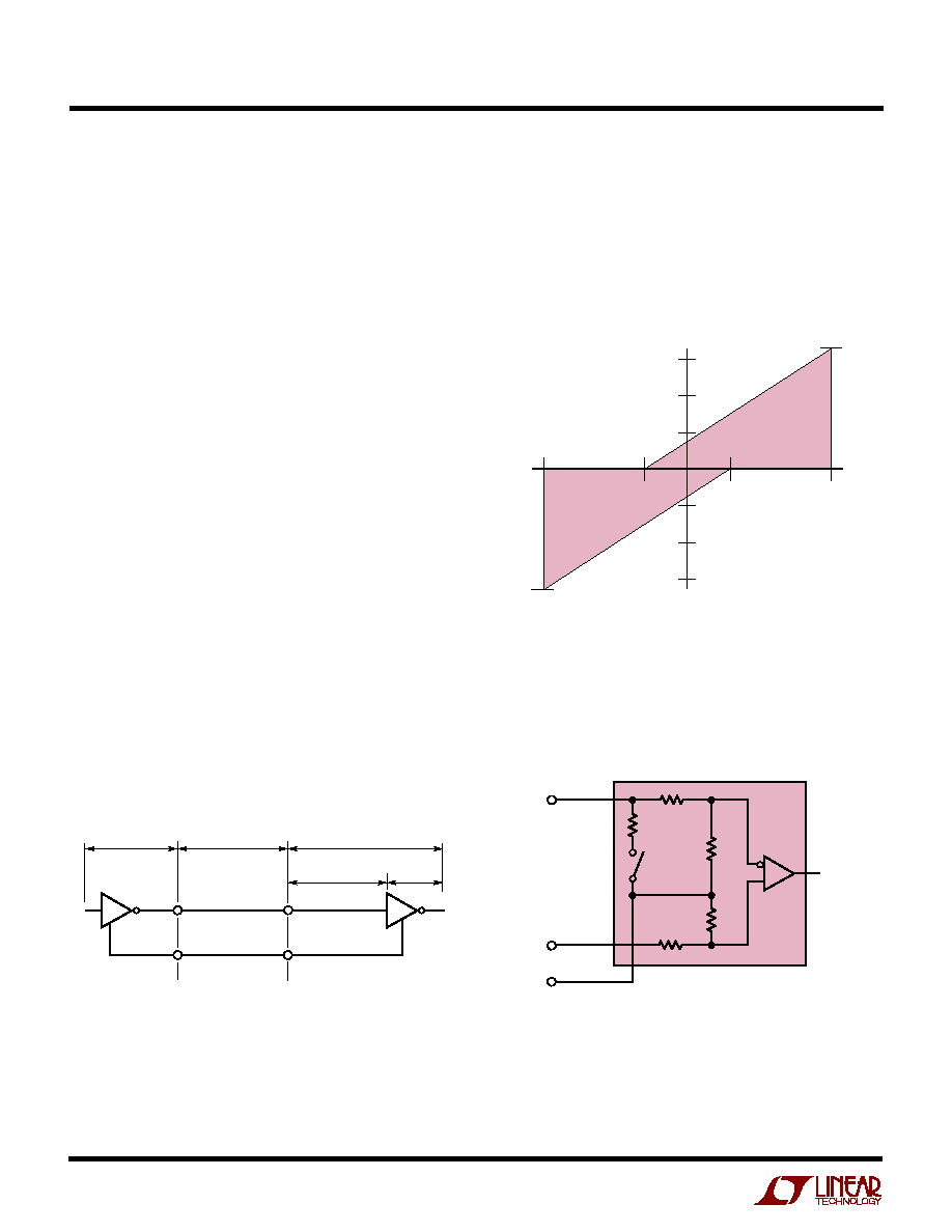
V.11
V.11
V.11
Z
V.11
V.11
Z
V.10
X.21
0
1
1
1
1
V.11
V.11
V.11
Z
V.11
V.11
Z
V.10
V.35
1
0
0
1
1
V.28
V.28
V.28
Z
V.28
V.28
Z
V.28
RS449/V.36
1
0
1
1
1
V.11
V.11
V.11
Z
V.11
V.11
Z
V.10
V.28/RS232
1
1
0
1
1
V.28
V.28
V.28
Z
V.28
V.28
Z
V.28
No Cable
1
1
1
1
1
Z
Z
Z
Z
Z
Z
Z
Z
ODE SELECTIO
W
U
TEST CIRCUITS
7
LTC1544
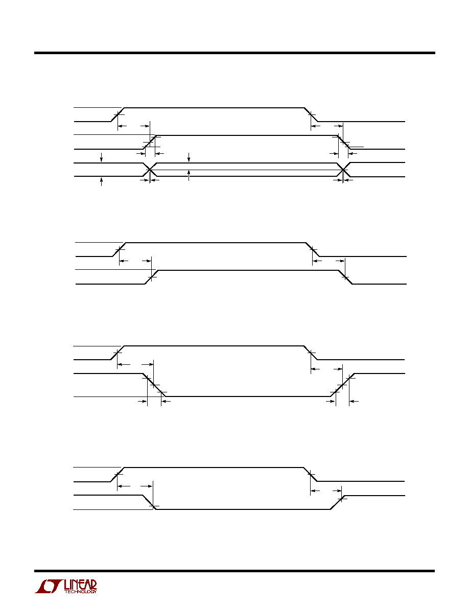
Figure 7. V.10, V.28 Driver Propagation Delays
Figure 6. V.11, V.35 Receiver Propagation Delays
Figure 8. V.10, V.28 Receiver Propagation Delays
3V
0V
1.5V
0V
≠3V
3V
1.5V
0V
3V
≠3V
t
PHL
t
f
V
O
≠V
O
D
A
t
PLH
t
r
1544 F07
V
OD2
≠V
OD2
0V
1.5V
0V
1.5V
t
PLH
V
OH
V
OL
B ≠ A
R
t
PHL
1544 F06
f = 1MHz : t
r
10ns : t
f
10ns
INPUT
OUTPUT
V
IH
V
IL
1.3V
0.8V
1.7V
2.4V
t
PHL
V
OH
V
OL
A
R
t
PLH
1544 F08
5V
1.5V
1.5V
50%
10%
90%
t
PLH
t
r
0V
V
O
V
O
≠V
O
D
B ≠ A
A
B
t
PHL
t
SKEW
t
SKEW
1544 F05
1/2 V
O
f = 1MHz : t
r
10ns : t
f
10ns
V
DIFF
= V(A) ≠ V(B)
50%
10%
90%
t
f
Figure 5. V.11, V.35 Driver Propagation Delays
SWITCHI G TI E WAVEFOR S
U
W
W
8
LTC1544
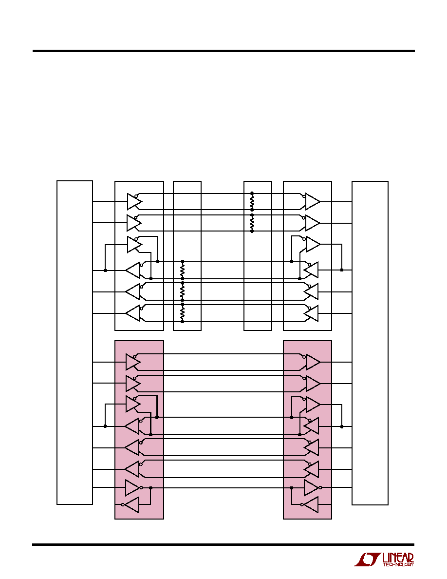
Overview
The LTC1543/LTC1544 form the core of a complete soft-
ware-selectable DTE or DCE interface port that supports
the RS232, RS449, EIA530, EIA530-A, V.35, V.36 or X.21
protocols. Cable termination may be implemented using
the LTC1344A software-selectable cable termination chip
or by using existing discrete designs.
A complete DCE-to-DTE interface operating in EIA530
mode is shown in Figure 9. The LTC1543 of each port is
used to generate the clock and data signals. The LTC1544
is used to generate the control signals along with LL (Local
Loop-back).The LTC1344A cable termination chip is used
only for the clock and data signals because they must
support V.35 cable termination. The control signals do not
need any external resistors.
Figure 9. Complete Multiprotocol Interface in EIA530 Mode
LTC1543
DCE
DTE
LTC1543
LTC1344A
LTC1344A
1544 F09
D3
D3
R1
103
103
103
R3
LTC1544
D4
R1
R2
R3
LL
TXC
RXC
RXD
TXD
SCTE
TXC
RXC
RXD
SERIAL
CONTROLLER
D2
103
SCTE
R2
D1
103
TXD
R3
R1
D2
D1
LTC1544
TXD
SCTE
TXC
RXC
RXD
RTS
DTR
DCD
DSR
CTS
LL
RTS
DTR
DCD
DSR
CTS
RTS
DTR
DCD
DSR
CTS
LL
SERIAL
CONTROLLER
R2
R4
R4
D3
D2
D1
R2
R1
R3
D2
D1
D4
D3
APPLICATIO
N
S I
N
FOR
M
ATIO
N
W
U
U
U
9
LTC1544
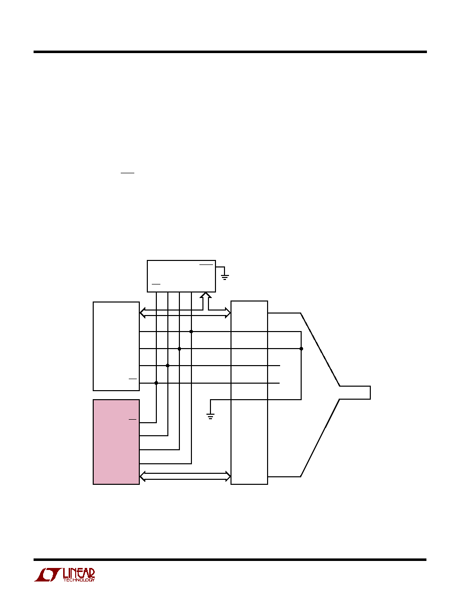
Mode Selection
The interface protocol is selected using the mode select
pins M0, M1 and M2 (see the Mode Selection table).
For example, if the port is configured as a V.35 interface,
the mode selection pins should be M2 = 1, M1 = 0, M0 = 0.
For the control signals, the drivers and receivers will
operate in V.28 (RS232) electrical mode. For the clock and
data signals, the drivers and receivers will operate in V.35
electrical mode. The DCE/DTE pin will configure the port
for DCE mode when high, and DTE when low.
The interface protocol may be selected simply by plug-
ging the appropriate interface cable into the connector.
The mode pins are routed to the connector and are left
unconnected (1) or wired to ground (0) in the cable as
shown in Figure 10.
The internal pull-up current sources will ensure a binary 1
when a pin is left unconnected and that the LTC1543/
LTC1544 and the LTC1344A enter the no-cable mode
when the cable is removed. In the no-cable mode the
LTC1543/LTC1544 supply current drops to less than
200
µ
A and all LTC1543/LTC1544 driver outputs and
LTC1344A resistive terminations are forced into a high
impedance state.
The mode selection may also be accomplished by using
jumpers to connect the mode pins to ground or V
CC
.
NC
NC
CABLE
1544 F10
11
12
13
14
LTC1543
LTC1544
CONNECTOR
14
13
12
11
22
21
M2
M1
LTC1344A
LATCH
M0 (DATA)
23
24
1
(DATA)
M0
M1
M2
DCE/DTE
DCE/DTE
M2
M1
M0
(DATA)
DCE/
DTE
Figure 10: Single Port DCE V.35 Mode Selection in the Cable
APPLICATIO
N
S I
N
FOR
M
ATIO
N
W
U
U
U
10
LTC1544
Cable Termination
Traditional implementations have included switching
resistors with expensive relays, or requiring the user to
change termination modules every time the interface
standard has changed. Custom cables have been used
with the termination in the cable head or separate termina-
tions are built on the board and a custom cable routes the
signals to the appropriate termination. Switching the
terminations with FETs is difficult because the FETs must
remain off even though the signal voltage is beyond the
supply voltage for the FET drivers or the power is off.
Using the LTC1344A along with the LTC1543/LTC1544
solves the cable termination switching problem. Via soft-
ware control, the LTC1344A provides termination for the
V.10 (RS423), V.11 (RS422), V.28 (RS232) and V.35
electrical protocols.
V.10 (RS423) Interface
A typical V.10 unbalanced interface is shown in Figure 11.
A V.10 single-ended generator output A with ground C is
connected to a differential receiver with inputs A
'
con-
nected to A, and input C
'
connected to the signal return
ground C. Usually, no cable termination is required for
V.10 interfaces, but the receiver inputs must be compliant
with the impedance curve shown in Figure 12.
The V.10 receiver configuration in the LTC1544 is shown
in Figure 13. In V.10 mode switch S3 inside the LTC1544
is turned off.The noninverting input is disconnected inside
the LTC1544 receiver and connected to ground. The cable
termination is then the 30k input impedance to ground of
the LTC1544 V.10 receiver.
I
Z
V
Z
≠10V
≠3.25mA
3.25mA
≠3V
3V
10V
1544 F12
Figure 12. V.10 Receiver Input Impedance
Figure 11. Typical V.10 Interface
Figure 13. V.10 Receiver Configuration
A
A
'
C
C
'
GENERATOR
BALANCED
INTERCONNECTING
CABLE
LOAD
CABLE
TERMINATION
RECEIVER
1544 F11
R5
20k
LTC1544
RECEIVER
1544 F13
A
B
A
'
B
'
C
'
R8
6k
S3
R6
10k
R7
10k
GND
R4
20k
APPLICATIO
N
S I
N
FOR
M
ATIO
N
W
U
U
U
11
LTC1544
V.11 (RS422) Interface
A typical V.11 balanced interface is shown in Figure 14. A
V.11 differential generator with outputs A and B with
ground C is connected to a differential receiver with
ground C
'
, inputs A
'
connected to A, B
'
connected to B. The
V.11 interface has a differential termination at the receiver
end that has a minimum value of 100
. The termination
resistor is optional in the V.11 specification, but for the
high speed clock and data lines, the termination is required
to prevent reflections from corrupting the data. The
receiver inputs must also be compliant with the imped-
ance curve shown in Figure 12.
In V.11 mode, all switches are off except S1 inside the
LTC1344A which connects a 103
differential termina-
tion impedance to the cable as shown in Figure 15.
R3
124
R5
20k
LTC1344A
LTC1543
LTC1544
RECEIVER
1544 F15
A
B
A
'
B
'
C
'
R1
51.5
R8
6k
S2
S3
R2
51.5
R6
10k
R7
10k
GND
R4
20k
S1
Figure 15. V.11 Receiver Configuration
A
A
'
B
C
B
'
C
'
GENERATOR
BALANCED
INTERCONNECTING
CABLE
LOAD
CABLE
TERMINATION
RECEIVER
100
MIN
1544 F14
V.28 (RS232) Interface
A typical V.28 unbalanced interface is shown in Figure 16.
A V.28 single-ended generator output A with ground C is
connected to a single-ended receiver with input A
'
con-
nected to A, ground C
'
connected via the signal return
ground C.
In V.28 mode all switches are off except S3 inside the
LTC1543/LTC1544 which connects a 6k (R8) impedance
to ground in parallel with 20k (R5) plus 10k (R6) for a
combined impedance of 5k as shown in Figure 17. The
noninverting input is disconnected inside the LTC1543/
LTC1544 receiver and connected to a TTL level reference
voltage for a 1.4V receiver trip point.
A
A
'
C
C
'
GENERATOR
BALANCED
INTERCONNECTING
CABLE
LOAD
CABLE
TERMINATION
RECEIVER
1544 F16
Figure 14. Typical V.11 Interface
R3
124
R5
20k
LTC1344A
LTC1543
LTC1544
RECEIVER
1544 F17
A
B
A
'
B
'
C
'
R1
51.5
R8
6k
S2
S3
R2
51.5
R6
10k
R7
10k
GND
R4
20k
S1
Figure 17. V.28 Receiver Configuration
Figure 16. Typical V.28 Interface
APPLICATIO
N
S I
N
FOR
M
ATIO
N
W
U
U
U
12
LTC1544
A
A
'
B
C
B
'
C
'
GENERATOR
BALANCED
INTERCONNECTING
CABLE
LOAD
CABLE
TERMINATION
RECEIVER
1544 F18
50
125
50
50
125
50
Figure 18. Typical V.35 Interface
R3
124
R5
20k
LTC1344A
LTC1543
RECEIVER
1544 F19
A
B
A
'
B
'
C
'
R1
51.5
R8
6k
S2
S3
R2
51.5
R6
10k
R7
10k
GND
R4
20k
S1
Figure 19. V.35 Receiver Configuration
V.35 Interface
A typical V.35 balanced interface is shown in Figure 18. A
V.35 differential generator with outputs A and B with
ground C is connected to a differential receiver with
ground C
'
, inputs A
'
connected to A, B
'
connected to B. The
V.35 interface requires a T or delta network termination at
the receiver end and the generator end. The receiver
differential impedance measured at the connector must be
100
±
10
, and the impedance between shorted termi-
nals (A
'
and B
'
)
and ground C
'
must be 150
±
15
.
In V.35 mode, both switches S1 and S2 inside the LTC1344A
are on, connecting the T network impedance as shown in
Figure 19. The switch in the LTC1543 is off. The 30k input
impedance of the receiver is placed in parallel with the T
network termination, but does not affect the overall input
impedance significantly.
APPLICATIO
N
S I
N
FOR
M
ATIO
N
W
U
U
U
13
LTC1544
Charge Pump
The LTC1543 uses an internal capacitive charge pump to
generate V
DD
and V
EE
as shown in Figure 21. A voltage
doubler generates about 8V on V
DD
and a voltage inverter
generates about ≠ 7.5V for V
EE
. Four 1
µ
F surface mounted
tantalum or ceramic capacitors are required for C1, C2, C3
and C4. The V
EE
capacitor C5 should be a minimum of
3.3
µ
F. All capacitors are 16V and should be placed as close
as possible to the LTC1543 to reduce EMI.
The generator differential impedance must be 50
to
150
and the impedance between shorted terminals (A
and B) and ground C must be 150
±
15
. For the
generator termination, switches S1 and S2 are both on and
the top side of the center resistor is brought out to a pin so
it can be bypassed with an external capacitor to reduce
common mode noise as shown in Figure 20.
Figure 20. V.35 Driver Using the LTC1344A
V.35 DRIVER
A
B
C
51.5
S2
ON
S1
ON
1544 F20
51.5
LTC1344A
124
C1
100pF
28
27
26
25
1544 F21
3
2
1
4
C3
1
µ
F
C4
1
µ
F
5V
C1
1
µ
F
C2
1
µ
F
C5
3.3
µ
F
LTC1543
V
DD
C1
+
C1
≠
V
CC
C2
+
C2
≠
V
EE
GND
+
Figure 21. Charge Pump
Any mismatch in the driver rise and fall times or skew in
the driver propagation delays will force current through
the center termination resistor to ground, causing a high
frequency common mode spike on the A and B terminals.
The common mode spike can cause EMI problems that are
reduced by capacitor C1 which shunts much of the com-
mon mode energy to ground rather than down the cable.
No-Cable Mode
The no-cable mode (M0 = M1 = M2 = 1) is intended for the
case when the cable is disconnected from the connector.
The charge pump, bias circuitry, drivers and receivers are
turned off, the driver outputs are forced into a high
impedance state, and the supply current drops to less than
200
µ
A.
Receiver Fail-Safe
All LTC1543/LTC1544 receivers feature fail-safe opera-
tion in all modes. If the receiver inputs are left floating or
shorted together by a termination resistor, the receiver
output will always be forced to a logic high.
DTE vs DCE Operation
The DCE/DTE pin acts as an enable for Driver 3/Receiver
1 in the LTC1543, and Driver 3/Receiver 1 and Driver 4/
Receiver 4 in the LTC1544. The INVERT pin in the LTC1544
allows the Driver 4/Receiver 4 enable to be high or low true
polarity.
APPLICATIO
N
S I
N
FOR
M
ATIO
N
W
U
U
U

14
LTC1544
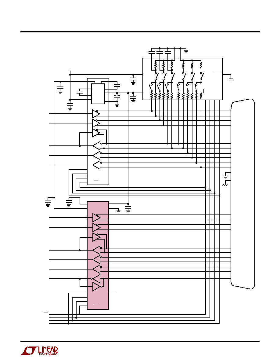
The LTC1543/LTC1544 can be configured for either DTE
or DCE operation in one of two ways: a dedicated DTE or
DCE port with a connector of appropriate gender or a port
with one connector that can be configured for DTE or DCE
operation by rerouting the signals to the LTC1543/LTC1544
using a dedicated DTE cable or dedicated DCE cable.
A dedicated DTE port using a DB-25 male connector is
shown in Figure 22. The interface mode is selected by logic
outputs from the controller or from jumpers to either V
CC
or GND on the mode select pins. A dedicated DCE port
using a DB-25 female connector is shown in Figure 23.
A port with one DB-25 connector, but can be configured
for either DTE or DCE operation is shown in Figure 24. The
configuration requires separate cables for proper signal
routing in DTE or DCE operation. For example, in DTE
mode, the TXD signal is routed to Pins 2 and 14 via Driver
1 in the LTC1543. In DCE mode, Driver 1 now routes the
RXD signal to Pins 2 and 14.
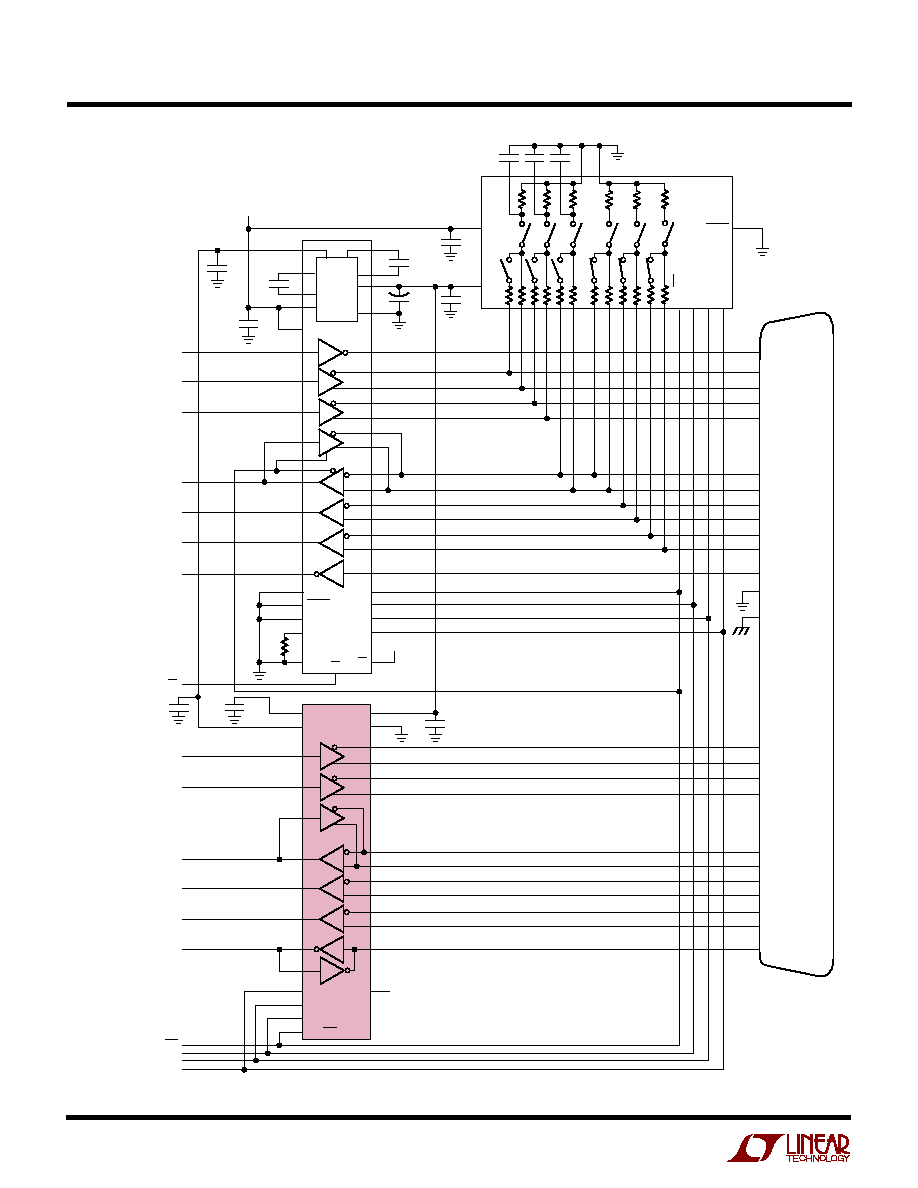
Multiprotocol Interface with RL, LL, TM and a DB-25
Connector
If the RL, LL and TM signals are implemented, there are not
enough drivers and receivers available in the LTC1543/
LTC1544. In Figure 25, the required control signals are
handled by the LTC1544 but the clock/data signals use the
LTC1343. The LTC1343 has an additional single-ended
driver/receiver pair that can handle two more optional
control signals such as TM and LL.
Cable-Selectable Multiprotocol Interface
A cable-selectable multiprotocol DTE/DCE interface is
shown in Figure 26. The select lines M0, M1 and DCE/DTE
are brought out to the connector. The mode is selected by
the cable by wiring M0 (connector Pin 18) and M1 (con-
nector Pin 21) and DCE/DTE (connector Pin 25) to ground
(connector Pin 7) or letting them float. If M0, M1 or DCE/
DTE is floating, internal pull-up current sources will pull
the signals to V
CC
. The select bit M2 is hard wired to V
CC
.
When the cable is pulled out, the interface will go into the
no-cable mode.
Compliance Testing
A European standard EN 45001 test report is available for
the LTC1543/LTC1544/LTC1344A chipset. A copy of the
test report is available from LTC or TUV Telecom Services
Inc. (formerly Detecon Inc.)
The title of the report is:
Test Report No. NET2/102201/97.
The address of TUV Telecom Services Inc. is:
TUV Telecom Services Inc.
Type Approval Division
1775 Old Highway 8, Ste 107
St. Paul, MN 55112 USA
Tel. +1 (612) 639-0775
Fax. +1 (612) 639-0873
APPLICATIO
N
S I
N
FOR
M
ATIO
N
W
U
U
U
15
LTC1544
Figure 22. Controller-Selectable Multiprotocol DTE Port with DB-25 Connector
D2
D1
LTC1544
RTS
DTR
DSR
DCD
CTS
D3
R2
R1
R4
R3
D2
LTC1543
LL
TXD
SCTE
TXC
RXC
RXD
M0
M1
M2
DCE/DTE
V
CC
V
DD
V
CC
V
EE
GND
2
21
14
24
11
15
12
17
9
3
1
4
19
20
8
23
10
6
22
5
13
18
7
16
1544 F22
D3
R2
R1
R3
D1
C2
1
µ
F
C1
1
µ
F
C5
1
µ
F
C3
1
µ
F
C4
3.3
µ
F
TXD A (103)
TXD B
SCTE A (113)
SCTE B
RXC A (115)
RXC B
RXD A (104)
RXD B
RTS A (105)
RTS B
DTR A (108)
DTR B
CTS A (106)
CTS B
LL A (141)
SG
SHIELD
DB-25 MALE
CONNECTOR
TXC A (114)
TXC B
DCD A (109)
DCD B
DSR A (107)
DSR B
D4
16
10
9
7
6
4
3
8
11
12
13
5
2
15 18 17 19 20 22
LTC1344A
LATCH
C6
100pF
C7
100pF
C8
100pF
V
CC
V
CC
5V
23 24
14
1
DCE/DTE
M2
M1
M0
CHARGE
PUMP
+
28
3
1
2
4
5
6
7
8
9
10
11
12
13
14
1
2
3
4
5
6
7
8
10
9
INVERT
15
16
17
18
19
20
21
22
23
24
25
NC
27
26
25
24
23
22
21
20
19
18
17
16
15
26
27
28
V
EE
M0
M1
M2
DCE/DTE
M2
M1
M0
11
12
13
14
C12
1
µ
F
C13
1
µ
F
C11
1
µ
F
C10
1
µ
F
C9
1
µ
F
TYPICAL APPLICATIO S
U
16
LTC1544
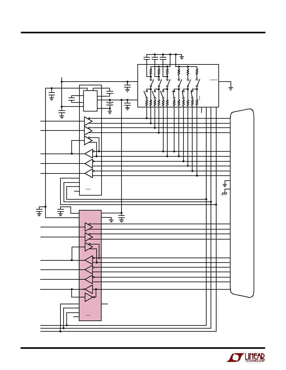
Figure 23. Controller-Selectable DCE Port with DB-25 Connector
D2
D1
LTC1544
CTS
DSR
DTR
DCD
RTS
D3
R2
R1
R4
R3
D2
LTC1543
LL
RXD
RXC
TXC
SCTE
TXD
M0
M1
M2
DCE/DTE
V
CC
V
DD
V
CC
V
EE
GND
3
16
17
9
15
12
24
11
2
1
5
13
6
8
22
10
20
23
4
19
18
7
14
1544 F23
D3
R2
R1
R3
D1
C2
1
µ
F
C1
1
µ
F
C5
1
µ
F
C3
1
µ
F
C4
3.3
µ
F
RXD A (104)
RXD B
RXC A (115)
RXC B
SCTE A (113)
SCTE B
TXD A (103)
TXD B
CTS A (106)
CTS B
DSR A (107)
DSR B
RTS A (105)
RTS B
LL A (141)
SGND (102)
SHIELD (101)
DB-25 FEMALE
CONNECTOR
TXC A (114)
TXC B
DCD A (109)
DCD B
DTR A (108)
DTR B
D4
16
10
9
7
6
4
3
8
11
12
13
5
2
15 18 17 19 20 22
LTC1344A
C6
100pF
C7
100pF
C8
100pF
V
CC
V
CC
V
CC
5V
23 24
14
1
DCE/DTE
M2
M1
M0
CHARGE
PUMP
+
28
3
1
2
4
5
6
7
8
9
10
NC
11
12
13
14
1
2
3
4
5
6
7
8
10
9
INVERT
15
16
17
18
19
20
21
22
23
24
25
NC
NC
27
26
25
24
23
22
21
20
19
18
17
16
15
26
27
28
V
EE
M0
M1
M2
DCE/DTE
M2
M1
M0
11
12
13
14
21
LATCH
C12
1
µ
F
C13
1
µ
F
C11
1
µ
F
C10
1
µ
F
C9
1
µ
F
TYPICAL APPLICATIO S
U
17
LTC1544
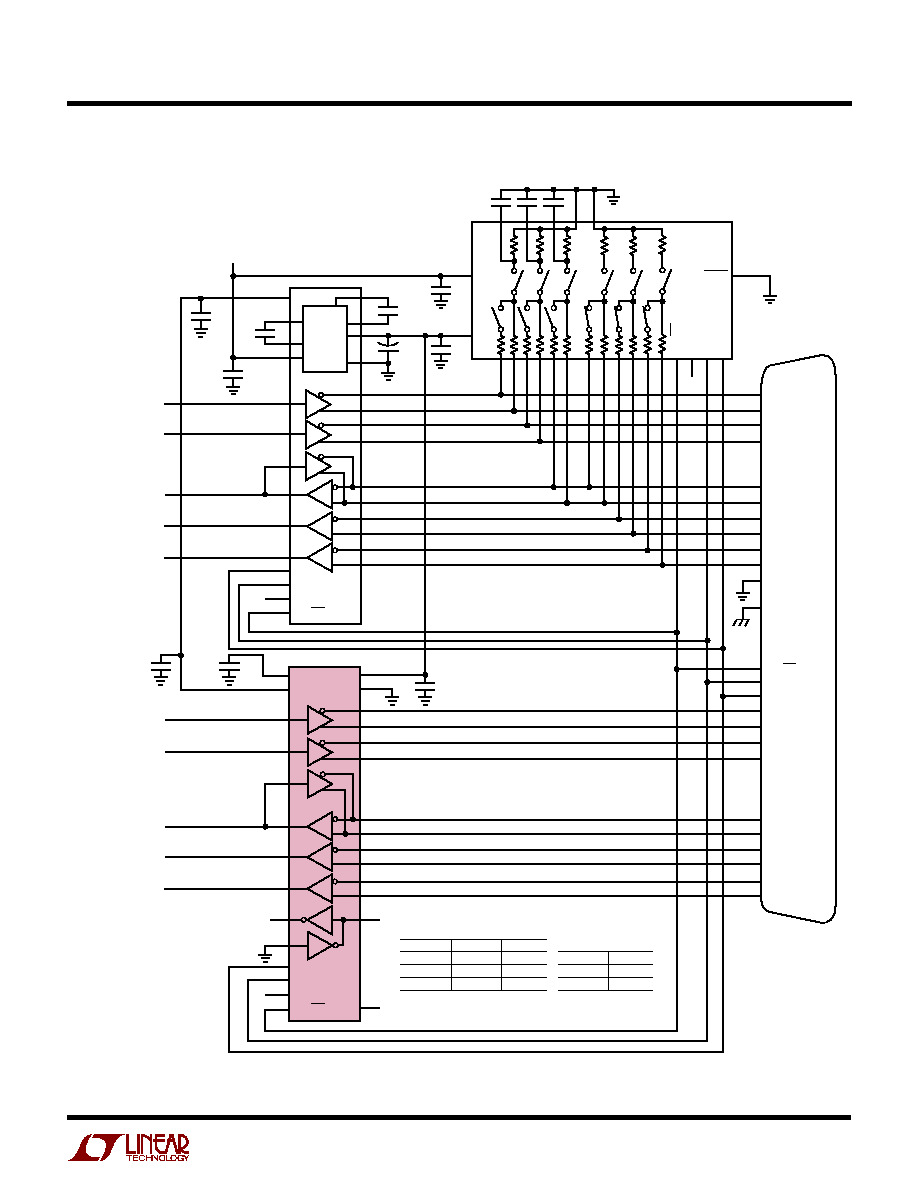
Figure 24. Controller-Selectable Multiprotocol DTE/DCE Port with DB-25 Connector
D2
D1
LTC1544
D3
R2
R1
R4
R3
D2
LTC1543
DTE_TXD/DCE_RXD
DTE_TXC/DCE_TXC
DTE_RXC/DCE_SCTE
DTE_RXD/DCE_TXD
DTE_RTS/DCE_CTS
DTE_DTR/DCE_DSR
DTE_DCD/DCE_DCD
DTE_DSR/DCE_DTR
DTE_CTS/DCE_RTS
DTE_LL/DCE_LL
DTE_SCTE/DCE_RXC
M0
M1
M2
DCE/DTE
V
CC
V
DD
V
CC
V
EE
GND
2
14
24
11
15
12
17
9
3
1
4
19
20
8
23
10
6
22
5
13
18
7
16
1544 F24
D3
R2
R1
R3
D1
C2
1
µ
F
C1
1
µ
F
C5
1
µ
F
C3
1
µ
F
C4
3.3
µ
F
TXD A
TXD B
SCTE A
SCTE B
RXD A
RXD B
RXC A
RXC B
RXC A
RXC B
RXD A
RXD B
RTS A
RTS B
DTR A
DTR B
CTS A
CTS B
DSR A
DSR B
CTS A
CTS B
LL A
SG
SHIELD
DB-25
CONNECTOR
TXC A
TXC B
SCTE A
SCTE B
TXD A
TXD B
TXC A
TXC B
DCD A
DCD B
DSR A
DSR B
RTS A
RTS B
LL A
DCD A
DCD B
DTR A
DTR B
D4
16
10
9
7
6
4
3
8
11
12
13
5
2
15 18 17 19 20 22
LTC1344A
C6
100pF
C7
100pF
C8
100pF
V
CC
V
CC
5V
23 24
14
1
DCE/DTE
M2
M1
M0
CHARGE
PUMP
+
28
3
1
2
4
5
6
7
8
9
10
11
12
13
14
1
2
3
4
5
6
7
8
10
9
INVERT
15
16
17
18
19
20
21
22
23
24
25
NC
27
26
25
24
23
22
21
20
19
18
17
16
15
26
27
28
V
EE
M0
M1
M2
DCE/DTE
DCE/DTE
M2
M1
M0
11
12
13
14
DTE
DCE
21
LATCH
C12
1
µ
F
C13
1
µ
F
C11
1
µ
F
C10
1
µ
F
C9
1
µ
F
TYPICAL APPLICATIO S
U
18
LTC1544
Figure 25. Controller-Selectable Multiprotocol DTE/DCE Port with RL, LL, TM and DB-25 Connector
D2
D1
LTC1544
D3
R2
R1
R4
R3
D2
LTC1343
DTE_LL/DCE_TM
DTE_TXC/DCE_TXC
DTE_RXC/DCE_SCTE
DTE_RXD/DCE_TXD
DTE_TM/DCE_LL
DTE_RTS/DCE_CTS
DTE_DTR/DCE_DSR
DTE_DCD/DCE_DCD
DTE_DSR/DCE_DTR
DTE_CTS/DCE_RTS
DTE_RL/DCE_RL
DTE_TXD/DCE_RXD
DTE_SCTE/DCE_RXC
CTRL
LATCH
INVERT
423SET
GND
DCE
M2
M1
M0
EC
V
CC
V
DD
V
CC
V
EE
GND
2
18
14
24
11
15
12
17
9
3
1
4
19
20
8
23
10
6
22
5
13
21
7
16
25
1544 F25
D3
D4
R2
R3
R4
D1
C2
1
µ
F
C1
1
µ
F
C5
1
µ
F
C3
1
µ
F
C4
3.3
µ
F
LL A
TXD A
TXD B
SCTE A
SCTE B
TM A
RXD A
RXD B
RXC A
RXC B
RXC A
RXC B
RXD A
RXD B
RTS A
RTS B
DTR A
DTR B
CTS A
CTS B
DSR A
DSR B
CTS A
CTS B
RL A
SG
SHIELD
DB-25
CONNECTOR
TXC A
TXC B
SCTE A
SCTE B
TXD A
TXD B
TXC A
TXC B
DCD A
DCD B
DSR A
DSR B
RTS A
RTS B
RL A
DCD A
DCD B
DTR A
DTR B
D4
16
10
9
7
6
4
3
8
11
12
13
5
2
15 18 17 19 20 22
LTC1344A
C6
100pF
C7
100pF
C8
100pF
V
CC
V
CC
5V
23 24
14
1
DCE/DTE
M2
M1
M0
CHARGE
PUMP
+
44
3
1
2
4
5
8
6
7
9
10
12
13
14
15
16
20
22
11
1
R1
100k
2
3
4
5
6
7
8
10
9
INVERT
15
16
17
18
19
20
21
22
23
24
25
NC
43
42
41
39
38
37
36
35
34
33
32
31
30
29
28
27
26
21
19
18
17
24
26
27
28
V
EE
M0
M1
M2
DCE/DTE
DCE/DTE
M2
M1
M0
11
12
13
14
DTE
DCE
R1
25
40
23
V
CC
LB
LB
TM A
LL A
21
LATCH
C12
1
µ
F
C13
1
µ
F
C11
1
µ
F
C10
1
µ
F
C9
1
µ
F
TYPICAL APPLICATIO S
U
19
LTC1544
D2
D1
LTC1544
D3
R2
R1
R4
R3
D2
LTC1543
DTE_TXD/DCE_RXD
DTE_TXC/DCE_TXC
DTE_RXC/DCE_SCTE
DTE_RXD/DCE_TXD
DTE_RTS/DCE_CTS
DTE_DTR/DCE_DSR
DTE_DCD/DCE_DCD
DTE_DSR/DCE_DTR
DTE_CTS/DCE_RTS
DTE_SCTE/DCE_RXC
M0
M1
M2
DCE/DTE
V
CC
V
DD
NC
NC
V
CC
V
EE
GND
2
V
CC
14
24
11
15
12
17
9
3
1
25
21
18
4
19
20
8
23
10
6
22
5
13
7
16
1544 F26
D3
R2
R1
R3
D1
C2
1
µ
F
C1
1
µ
F
C5
1
µ
F
C3
1
µ
F
C4
3.3
µ
F
TXD A
TXD B
SCTE A
SCTE B
RXD A
RXD B
RXC A
RXC B
RXC A
RXC B
RXD A
RXD B
RTS A
RTS B
DTR A
DTR B
CTS A
CTS B
DSR A
DSR B
CTS A
CTS B
SG
SHIELD
DCE/DTE
M1
M0
DB-25
CONNECTOR
TXC A
TXC B
SCTE A
SCTE B
TXD A
TXD B
TXC A
TXC B
DCD A
DCD B
DSR A
DSR B
RTS A
RTS B
DCD A
DCD B
DTR A
DTR B
D4
16
10
9
7
6
4
3
8
11
12
13
5
2
15 18 17 19 20 22
LTC1344A
C6
100pF
C7
100pF
C8
100pF
V
CC
V
CC
5V
23 24
14
1
DCE/DTE
M2
M1
M0
CHARGE
PUMP
+
28
3
1
2
4
5
6
7
8
9
10
11
12
13
14
1
2
3
4
5
6
7
8
9
10
INVERT
15
17
16
18
19
20
21
22
23
24
25
NC
27
26
25
24
23
22
21
20
19
18
17
16
15
26
27
28
V
EE
M0
M1
M2
DCE/DTE
11
12
13
14
DTE
DCE
MODE
PIN 18
PIN 21
V.35
PIN 7
PIN 7
RS449, V.36
NC
PIN 7
RS232
PIN 7
NC
CABLE WIRING FOR MODE SELECTION
MODE
PIN 25
DTE
PIN 7
DCE
NC
CABLE WIRING FOR
DTE/DCE SELECTION
21
LATCH
C12
1
µ
F
C13
1
µ
F
C11
1
µ
F
C10
1
µ
F
C9
1
µ
F
Information furnished by Linear Technology Corporation is believed to be accurate and reliable.
However, no responsibility is assumed for its use. Linear Technology Corporation makes no represen-
tation that the interconnection of its circuits as described herein will not infringe on existing patent rights.
Figure 26. Cable-Selectable Multiprotocol DTE/DCE Port with DB-25 Connector
TYPICAL APPLICATIO S
U
20
LTC1544
1544fa LT/TP 0100 2K REV A ∑ PRINTED IN USA
©
LINEAR TECHNOLOGY CORPORATION 1998
RELATED PARTS
PART NUMBER
DESCRIPTION
COMMENTS
LTC1321
Dual RS232/RS485 Transceiver
Two RS232 Driver/Receiver Pairs or Two RS485 Driver/Receiver Pairs
LTC1334
Single 5V RS232/RS485 Multiprotocol Transceiver
Two RS232 Driver/Receiver or Four RS232 Driver/Receiver Pairs
LTC1343
Software-Selectable Multiprotocol Transceiver
4-Driver/4-Receiver for Data and Clock Signals
LTC1344A
Software-Selectable Cable Terminator
Perfect for Terminating the LTC1543
LTC1345
Single Supply V.35 Transceiver
3-Driver/3-Receiver for Data and Clock Signals
LTC1346A
Dual Supply V.35 Transceiver
3-Driver/3-Receiver for Data and Clock Signals
LTC1543
Software-Selectable Multiprotocol Transceiver
Companion to LTC1544 for Data and Clock Signals
LTC1546
Multiprotocol Transceiver with Termination
Companion to LTC1544 for Data and Clock Signals
Dimensions in inches (millimeters) unless otherwise noted.
G28 SSOP 1098
0.13 ≠ 0.22
(0.005 ≠ 0.009)
0
∞
≠ 8
∞
0.55 ≠ 0.95
(0.022 ≠ 0.037)
5.20 ≠ 5.38**
(0.205 ≠ 0.212)
7.65 ≠ 7.90
(0.301 ≠ 0.311)
1
2 3
4
5
6 7 8
9 10 11 12
14
13
10.07 ≠ 10.33*
(0.397 ≠ 0.407)
25
26
22 21 20 19 18 17 16 15
23
24
27
28
1.73 ≠ 1.99
(0.068 ≠ 0.078)
0.05 ≠ 0.21
(0.002 ≠ 0.008)
0.65
(0.0256)
BSC
0.25 ≠ 0.38
(0.010 ≠ 0.015)
NOTE: DIMENSIONS ARE IN MILLIMETERS
DIMENSIONS DO NOT INCLUDE MOLD FLASH. MOLD FLASH
SHALL NOT EXCEED 0.152mm (0.006") PER SIDE
DIMENSIONS DO NOT INCLUDE INTERLEAD FLASH. INTERLEAD
FLASH SHALL NOT EXCEED 0.254mm (0.010") PER SIDE
*
**
G Package
28-Lead Plastic SSOP (0.209)
(LTC DWG # 05-08-1640)
Linear Technology Corporation
1630 McCarthy Blvd., Milpitas, CA 95035-7417
(408) 432-1900
q
FAX: (408) 434-0507
q
www.linear-tech.com
U
PACKAGE DESCRIPTIO