LTC1555L-1.8
1
APPLICATIO S
U
FEATURES
DESCRIPTIO
U
TYPICAL APPLICATIO
U
The LTC
Æ
1555L-1.8 provides power conversion and level
shifting needed for low voltage GSM and WCDMA cellular
telephones to interface with either 1.8V, 3V or 5V sub-
scriber identity modules (SIMs). The part contains a
patented buck/boost charge pump DC/DC converter* that
delivers a regulated V
CC
supply voltage to the SIM card.
Input voltage may range from 2.6V to 6V allowing direct
connection to the battery. The output voltage may be
programmed to 1.8V, 3V, 5V or direct connection to the
V
IN
pin.
Internal level translators allow controllers operating with
supplies as low as 1.425V to interface with 1.8V, 3V and
5V SIMs. A soft-start feature limits inrush current at turn-
on, mitigating start-up problems that may result when the
input is supplied by another low-power DC/DC converter.
Battery life is maximized by 32
µ
A operating current, and
1
µ
A shutdown current. Board area is minimized by the
miniature 16-pin narrow SSOP packages and the need for
only three small external capacitors.
s
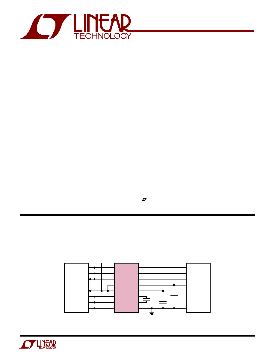
SIM Interface in GSM Cellular Telephones
s
WCDMA SIM Interface
s
Smart Card Readers
, LTC and LT are registered trademarks of Linear Technology Corporation.
SIM Power Supply and
Level Translator
s
Buck/Boost Charge Pump Generates 1.8V, 3V or 5V
s
Input Voltage Range: 2.6V to 6V
s
Controller V
CC
Range: 1.425V to 4.4V
s
>10kV ESD on All SIM Contact Pins
s
Short-Circuit and Overtemperature Protected
s
Meets all ETSI and IMT-2000 SIM Interface
Requirements
s
1.8V to 5V Signal Level Translators
s
Very Low Operating Current: 32
µ
A
s
Very Low Shutdown Current: <1
µ
A
s
Soft-Start Limits Inrush Current at Turn-On
s
1MHz Switching Frequency
s
Available in 16-Pin Narrow SSOP Package
GSM Cellular Telephone SIM Interface
1
2
3
4
5
6
7
8
16
15
14
13
12
11
10
9
CIN
RIN
DATA
DDRV
DV
CC
M2
M1
M0
CLK
RST
I/O
V
CC
= 1.8V,3V,5V
I
VCC
=
10mA
GND
CLK
RST
I/O
V
CC
V
IN
C1
+
C1
≠
GND
0.1
µ
F
1
µ
F
LTC1555L-1.8
GSM
CONTROLLER
SIM
V
IN
2.6V TO 6V
1.425V TO 4.4V
2.2
µ
F
1555L TA01
V
CC
*U.S. Patent No.: 5,973,944
LTC1555L-1.8
2
V
IN
, DV
CC
to GND ..................................... ≠0.3V to 6.5V
V
CC
to GND ............................................... ≠ 0.3V to 6.5V
Digital Inputs to GND ................................≠ 0.3V to 6.5V
CLK, RST, I/O to GND ..................... ≠ 0.3V to V
CC
+ 0.3V
V
CC
Short-Circuit Duration ............................... Indefinite
Operating Temperature Range (Note 2) .. ≠ 40
∞
C to 85
∞
C
Storage Temperature Range ................. ≠ 65
∞
C to 150
∞
C
Lead Temperature (Soldering,10 sec)................... 300
∞
C
ORDER PART
NUMBER
T
JMAX
= 125
∞
C,
JA
= 150
∞
C/W
LTC1555LEGN-1.8
ABSOLUTE AXI U
RATI GS
W
W
W
U
PACKAGE/ORDER I FOR ATIO
U
U
W
(Note 1)
ELECTRICAL CHARACTERISTICS
The
q
denotes the specifications which apply over the full operating
temperature range, otherwise specifications are at T
A
= 25
∞
C. (V
IN
= 2.6V to 6V, DV
CC
= 1.425V to 4.4V, controller digital pins tied to
DV
CC
, SIM digital pins floating, C1 = 0.1
µ
F, C
OUT
= 2.2
µ
F unless otherwise noted)
PARAMETER
CONDITIONS
MIN
TYP
MAX
UNITS
V
IN
Operating Voltage
q
2.6
6
V
DV
CC
Operating Voltage
q
1.425
4.4
V
DV
CC
Undervoltage Lockout
1.2
V
V
IN
Operating Current
V
CC
= 3V, I
VCC
= 0V
q
27
65
µ
A
V
IN
Shutdown Current
M0, M1 = 0V
q
1
µ
A
DV
CC
Operating Current
M0, M1, DATA = DV
CC
, C
IN
= 1MHz
q
5
30
µ
A
DV
CC
Shutdown Current
M0, M1 = 0V, DATA, C
IN
= DV
CC
q
1
µ
A
V
CC
Output Voltage
0 < I
VCC
< 10mA
M0, M1 = DV
CC
, 2.6V < V
IN
< 6V
q
4.55
5
5.25
V
M0, M1 = DV
CC
, 2.7V < V
IN
< 6V
q
4.75
5
5.25
V
M0 = DV
CC
, M1 = 0
q
2.8
3
3.2
V
M0 = 0, M1 = DV
CC
q
V
IN
≠ 0.2
V
IN
V
M0 = DV
CC
, M1 = 0, M2 = DV
CC
, 0
I
VCC
6mA
q
1.71
1.8
1.89
V
M0 = DV
CC
, M1 = 0, M2 = DV
CC
, V
IN
3V, I
VCC
10mA
q
1.71
1.8
1.89
V
V
CC
Short-Circuit Current
V
CC
Shorted to GND
q
50
150
mA
Charge Pump f
OSC
1
MHz
TOP VIEW
GN PACKAGE
16-LEAD PLASTIC SSOP
1
2
3
4
5
6
7
8
16
15
14
13
12
11
10
9
CIN
RIN
DATA
DDRV
DV
CC
M2
M1
M0
CLK
RST
I/0
V
CC
V
IN
C1
+
C1
≠
GND
GN PART MARKING
555L18
Consult factory for parts specified with wider operating temperature ranges.

LTC1555L-1.8
3
PARAMETER
CONDITIONS
MIN
TYP
MAX
UNITS
Controller Inputs/Outputs (DV
CC
= 1.8V)
Input Current (I
IH
/I
IL
)
M0, M1, M2, RIN, CIN
q
≠100
100
nA
Input Current (I
IH
/I
IL
)
DDRV
q
≠5
5
µ
A
High Level Input Current (I
IH
)
DATA
q
≠20
20
µ
A
Low Level Input Current (I
IL
)
DATA
q
1
mA
High Input Voltage Threshold (V
IH
)
M0, M1, M2, RIN, CIN, DDRV
q
0.7
◊
DV
CC
V
DATA
q
DV
CC
≠ 0.6
V
Low Input Voltage Threshold (V
IL
)
M0, M1, M2, RIN, CIN, DDRV
q
0.2
◊
DV
CC
V
DATA
q
0.4
V
High Level Output Voltage (V
OH
)
DATA Source Current = 20
µ
A I/O = V
CC
q
0.7
◊
DV
CC
V
Low Level Output Voltage (V
OL
)
DATA Sink Current = ≠200
µ
A I/O = 0V (Note 3)
q
0.4
V
DATA Pull-Up Resistance
Between DATA and DV
CC
q
13
20
30
k
DATA Output Rise/Fall Time
DATA Loaded with 30pF
q
1.3
2
µ
s
SIM Inputs/Outputs (V
CC
= 3V or 5V)
I/O High Input Voltage Threshold (V
IH
)
I
IH(MAX)
=
±
20
µ
A
q
0.7
◊
V
CC
V
I/O Low Input Voltage Threshold (V
IL
)
I
IL(MAX)
= 1mA
q
0.4
V
High Level Output Voltage (V
OH
)
I/O, Source Current = 20
µ
A DATA or DDRV = DV
CC
q
0.8
◊
V
CC
V
Low Level Output Voltage (V
OL
)
I/O, Sink Current = ≠1mA DATA or DDRV = 0V (Note 3)
q
0.4
V
High Level Output Voltage (V
OH
)
RST, CLK Source Current = 20
µ
A
q
0.9
◊
V
CC
V
Low Level Output Voltage (V
OL
)
RST, CLK Sink Current = ≠200
µ
A
q
0.4
V
I/O Pull-Up Resistance
Between I/O and V
CC
q
6.5
10
14
k
SIM Inputs/Outputs (V
CC
= 1.8V)
I/O High Input Voltage Threshold (V
IH
)
I
IH(MAX)
=
±
20
µ
A
q
0.7
◊
V
CC
V
I/O Low Input Voltage Threshold (V
IL
)
I
IL(MAX)
= 1mA
q
0.2
◊
V
CC
V
High Level Output Voltage (V
OH
)
I/O, Source Current = 20
µ
A DATA or DDRV = DV
CC
q
0.8
◊
V
CC
V
Low Level Output Voltage (V
OL
)
I/O, Sink Current = ≠200
µ
A DATA or DDRV = 0V (Note 3)
q
0.4
V
High Level Output Voltage (V
OH
)
RST, CLK Source Current = 20
µ
A
q
0.9
◊
V
CC
V
Low Level Output Voltage (V
OL
)
RST, CLK Sink Current = ≠200
µ
A
q
0.2
◊
V
CC
V
SIM Timing Parameters (DV
CC
= 1.8V, V
CC
= 5V)
CLK Rise/Fall Time
CLK Loaded with 30pF, V
CC
= 3V or 5V
q
18
ns
V
CC
= 1.8V
q
50
ns
RST, I/O Rise/Fall Time
RST, I/O Loaded with 30pF
q
1
µ
s
CLK Frequency
CLK Loaded with 30pF
q
5
MHz
V
CC
Turn-On Time
C
OUT
= 2.2
µ
F, I
VCC
= 0
0.5
ms
V
CC
Discharge Time to 1V
I
VCC
= 0, V
CC
= 5V, C
OUT
= 2.2
µ
F
0.5
ms
Note 1: Absolute Maximum Ratings are those values beyond which the life
of a device may be impaired.
Note 2: The LTC1555LEGN-1.8 is guaranteed to meet performance
specifications from 0
∞
C to 70
∞
C. Specifications over the ≠ 40
∞
C to 85
∞
C
operating temperature range are assured by design, characterization and
correlation with statistical process controls.
Note 3: The DATA and I/O pull-down drivers must also sink current
sourced by the internal pull-up resistor.
The
q
denotes the specifications which apply over the full operating
temperature range, otherwise specifications are at T
A
= 25
∞
C. (V
IN
= 2.6V to 6V, DV
CC
= 1.425V to 4.4V, controller digital pins tied to
DV
CC
, SIM digital pins floating, C1 = 0.1
µ
F, C
OUT
= 2.2
µ
F unless otherwise noted)
ELECTRICAL CHARACTERISTICS
LTC1555L-1.8
4
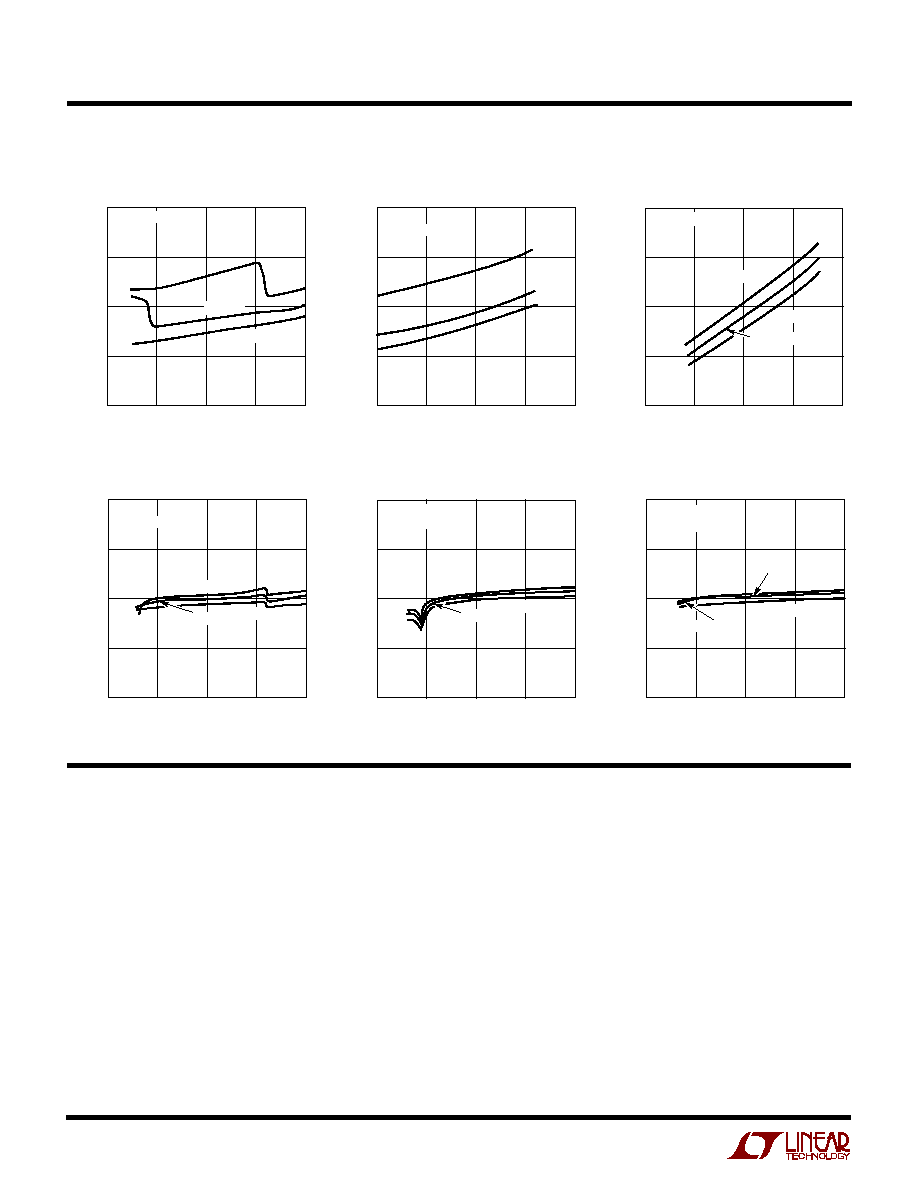
TYPICAL PERFOR A CE CHARACTERISTICS
U
W
V
IN
(V)
2
I
VIN
(
µ
A)
30
40
6
1555L ∑ G01
20
10
3
4
5
50
V
CC
= 5V
V
CC
= 3V
V
CC
= 1.8V
I
VCC
= 0mA
T
A
= 25
∞
C
TEMPERATURE (
∞
C)
≠40
I
VIN
(
µ
A)
30
40
120
1555L ∑ G02
20
10
0
40
80
50
V
CC
= 5V
V
CC
= 3V
V
CC
= 1.8V
V
IN
= 3.6V
I
VCC
= 0mA
V
DVCC
(V)
1
I
DVCC
(
µ
A)
10
15
5
1555L ∑ G03
5
0
2
3
4
20
F
CLK
= 1MHz
T
A
= ≠40
∞
C
T
A
= 85
∞
C
T
A
= 25
∞
C
V
IN
(V)
2
V
CC
(V)
5.0
5.5
6
1555L ∑ G04
4.5
4.0
3
4
5
6.0
V
CC
= 5V
I
VCC
= 10mA
T
A
= ≠40
∞
C
T
A
= 85
∞
C
T
A
= 25
∞
C
V
IN
(V)
2
V
CC
(V)
3.0
3.3
6
1555L ∑ G05
2.7
2.4
3
4
5
3.6
T
A
= ≠40
∞
C
T
A
= 85
∞
C
V
CC
= 3V
I
VCC
= 10mA
T
A
= 25
∞
C
V
IN
(V)
2
V
CC
(V)
1.8
2.0
6
1555L ∑ G06
1.6
1.4
3
4
5
2.2
T
A
= ≠40
∞
C
V
CC
= 1.8V
I
VCC
= 10mA
T
A
= 85
∞
C
T
A
= 25
∞
C
I
VIN
vs V
IN
V
CC
vs V
IN
I
VIN
vs Temperature
I
DVCC
vs V
DVCC
V
CC
vs V
IN
V
CC
vs V
IN
PI
N
FU
N
CTIO
N
S
U
U
U
CIN (Pin 1): Clock Input Pin from Controller.
RIN (Pin 2): Reset Input Pin from Controller.
DATA (Pin 3): Controller Side Data Input/Output Pin. Can
be used for single pin bidirectional data transfer between
the controller and the SIM card as long as the controller
data pin is open drain. The controller output must be able
to sink 1mA max when driving the DATA pin low due to the
internal pull-up resistors on the DATA and I/O pins. If the
controller data output is not open drain, then the DDRV pin
should be used for sending data to the SIM card and the
DATA pin used for receiving data from the SIM card.
DDRV (Pin 4): Optional Data Input Pin for Sending Data to
the SIM Card. When not needed, the DDRV pin should
either be left floating or tied to DV
CC
(an internal 1
µ
A
current source will pull the DDRV pin up to DV
CC
if left
floating).
DV
CC
(Pin 5): Supply Voltage for Controller Side Digital
Input/Output Pins (typically 3V). May be between 1.425V
and 4.4V. The DV
CC
supply may be powered-down in
shutdown for further reduction in battery current. When
DV
CC
drops below 1.2V, the charge pump is disabled and
the LTC1555L-1.8 goes into shutdown mode regardless
of the signals on the M0-M2 pins.
LTC1555L-1.8
5
V
IN
(Pin 12): Charge Pump Input Pin. May be between 2.6V
and 6V. There is no power-up sequencing requirement for
V
IN
with respect to DV
CC
.
V
CC
(Pin 13): SIM Card V
CC
Output. Should be connected
to the SIM V
CC
contact. The V
CC
output voltage is deter-
mined by the M0-M2 pins (see Table 1). V
CC
is discharged
to GND during shutdown (M0, M1 = 0V). A 2.2
µ
F low ESR
ouptut capacitor should connect close to the V
CC
pin.
I/O (Pin 14): SIM Side I/O Pin. The pin is an open drain
output with a nominal pull-up resistance of 10k
and
should be connected to the SIM I/O contact. The SIM card
must sink up to 1mA max when driving the I/O pin low due
to the internal pull-up resistors on the I/O and DATA pins.
The I/O pin is held active low during shutdown.
RST (Pin 15): Level Shifted Reset Output Pin. Should be
connected to the SIM RST contact.
CLK (Pin 16): Level Shifted Clock Output Pin. Should be
connected to the SIM CLK contact. Careful trace routing is
recommended due to fast rise and fall edge speeds.
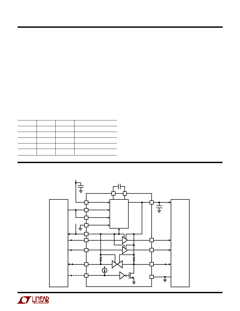
M0
M1
M2
OPERATING MODE
0V
0V
0V or DV
CC
Shutdown (V
CC
= 0V)
0V
DV
CC
0V or DV
CC
V
CC
= V
IN
DV
CC
0V
0V
V
CC
= 3V
DV
CC
0V
DV
CC
V
CC
= 1.8V
DV
CC
DV
CC
0V or DV
CC
V
CC
= 5V
Table 1. Truth Table
PI
N
FU
N
CTIO
N
S
U
U
U
M2 (Pin 6): Mode Control Bit 2 (see Table 1). (Pin 6 was
previously used for soft-start control on the LTC1555.)
M1 (Pin 7): Mode Control Bit 1 (see Table 1).
M0 (Pin 8): Mode Control Bit 0 (see Table 1).
GND (Pin 9): Ground for Both the SIM and the Controller.
Should be connected to the SIM GND contact as well as to
the V
IN
/controller GND. Proper grounding and supply
bypassing is required to meet 10kV ESD specifications.
C1
≠
(Pin 10): Charge Pump Flying Capacitor Negative Input.
C1
+
(Pin 11): Charge Pump Flying Capacitor Positive Input.
BLOCK DIAGRA
W
DDRV
OPTIONAL
1
µ
A
I/O
DATA
20k
10k
CLK
CIN
RST
DV
CC
M2
1.8V
RIN
GND
M1
M0
V
IN
V
BATT
C
IN
1
µ
F
V
CC
I/O
CLK
RST
GND
V
CC
C1
+
0.1
µ
F
C1
≠
STEP-UP/
STEP-DOWN
CHARGE PUMP
DC/DC
CONVERTER
SIM
CONTROLLER
V
CC
C
OUT
2.2
µ
F
UVLO
LTC1555L-1.8
1555L BD

LTC1555L-1.8
6
APPLICATIO S I FOR ATIO
W
U
U
U
The LTC1555L-1.8 performs the two primary functions
necessary for low voltage controllers (e.g., GSM cellular
telephone controllers, smart card readers, etc.) to com-
municate with 5V SIMs or smart cards. The part produces
a regulated 1.8V, 3V or 5V V
CC
supply for the SIM, and also
provides level translators for communication between the
SIM and the controller.
V
CC
Voltage Regulator
The regulator section of the LTC1555L-1.8 (refer to Block
Diagram) consists of a buck/boost charge pump DC/DC
converter. The charge pump can operate over a wide input
voltage range (2.6V to 6V) while maintaining a regulated
V
CC
output. The wide V
IN
range enables the part to be
powered directly from a battery (if desired) rather than
from a DC/DC converter output. When V
IN
is less than the
selected V
CC
voltage, the part operates as a switched
capacitor voltage doubler. When V
IN
is greater than V
CC
,
the part operates as gated switch step-down converter. In
either case, voltage conversion requires only one small
flying capacitor and output capacitor.
The V
CC
output can be programmed via the M0-M2 pins to
either 1.8V, 3V, 5V or direct connection to V
IN
. This
flexibility is useful in applications where multiple voltage
SIMs may be used. When the charge pump is put into
shutdown (M0, M1 = 0), V
CC
is pulled to GND via an
internal switch to aid in proper system supply sequencing.
An internal soft-start feature helps to limit inrush currents
upon start-up or when coming out of shutdown mode.
Inrush current limiting is especially useful when powering
the LTC1555L-1.8 from a DC/DC output since the unlim-
ited inrush current may approach 300mA and cause
voltage transients on the 3V supply. The part is fully short-
circuit and over temperature protected, and can survive an
indefinite short from V
CC
to GND.
Capacitor Selection
For best performance, it is recommended that low ESR
(< 0.5
) capacitors be used for both C
IN
and C
OUT
to reduce
noise and ripple. The C
IN
and C
OUT
capacitors should be
either ceramic or tantalum and should be 1
µ
F or greater
(ceramic capacitors will produce the smallest output ripple).
If the input source impedance is very low (< 0.5
), C
IN
may
not be needed. Increasing the size of C
OUT
to 2.2
µ
F or greater
will reduce output voltage ripple--particularly with high V
IN
voltages (4V or greater). A ceramic capacitor is recom-
mended for the flying capacitor C1 with a value of 0.1
µ
F or
0.22
µ
F.
Output Ripple
Normal LTC1555L-1.8 operation produces voltage ripple
on the V
CC
pin. Output voltage ripple is required for the
parts to regulate. Low frequency ripple exists due to the
hysteresis in the sense comparator and propagation de-
lays in the charge pump enable/disable circuits. High
frequency ripple is also present mainly from the ESR
(equivalent series resistance) in the output capacitor.
Typical output ripple (V
IN
< 4V) under maximum load is
75mV peak-to-peak with a low ESR, 2.2
µ
F output capaci-
tor (V
CC
= 5V).
The magnitude of the ripple voltage depends on several
factors. High input voltages increase the output ripple
since more charge is delivered to C
OUT
per charging cycle.
A large C1 flying capacitor (> 0.22
µ
F) also increases ripple
in step-up mode for the same reason. Large output current
load and/or a small output capacitor (< 1
µ
F) results in
higher ripple due to higher output voltage dV/dt. High ESR
capacitors (ESR > 0.5
) on the output pin cause high
frequency voltage spikes on V
OUT
with every clock cycle.
A 2.2
µ
F ceramic capacitor on the V
CC
pin should produce
acceptable levels of output voltage ripple in nearly all
applications. Also, in order to keep noise down all capaci-
tors should be placed close to LTC1555L-1.8.
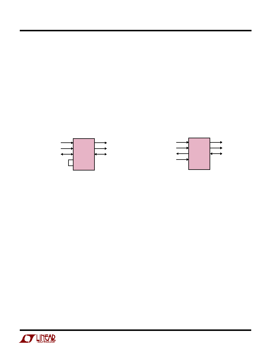
Level Translators
All SIMs and smart cards contain a clock input, a reset
input, and a bidirectional data input/output. The
LTC1555L-1.8 provides level translators to allow
controllers to communicate with the SIM. (See Figure 1a
and 1b). The CLK and RST inputs to the SIM are level
shifted from the controller supply rails (DV
CC
and GND) to
the SIM supply rails (V
CC
and GND). The data input to the
SIM may be provided two different ways. The first method
is to use the DATA pin as a bidirectional level translator.
LTC1555L-1.8
7
APPLICATIO S I FOR ATIO
W
U
U
U
This configuration is only allowed if the controller data
output pin is open drain (all SIM I/O pins are open drain).
Internal pull-up resistors are provided for both the DATA
pin and the I/O pin on the SIM side. The second method
is to use the DDRV pin to send data to the SIM and use the
DATA pin to receive data from the SIM. When the DDRV
pin is not used, it should either be left floating or tied to
DV
CC
.
Shutting Down the DV
CC
Supply
To conserve power, the DV
CC
supply may be shut down
while the V
IN
supply is still active. When the DV
CC
supply
is forced below 1.2V, an undervoltage lockout circuit
forces the LTC1555L-1.8 into shutdown mode regardless
of the status of the M0-M2 pins.
10kV ESD Protection
All pins that connect to the SIM (CLK, RST, I/O, V
CC
, GND)
withstand over 10kV of human body model ESD. In order
to ensure proper ESD protection, careful board layout is
required. The GND pin should be tied directly to a GND
plane. The V
CC
capacitor should be located very close to
the V
CC
pin and tied immediately to the GND plane.
CIN
RIN
DATA
DDRV
DV
CC
CLK
RST
I/O
V
CC
CLK TO SIM
RST TO SIM
DATA TO/FROM SIM
LTC1555L-1.8
CONTROLLER
SIDE
SIM SIDE
1555L F01a
Figure 1a. Level Translator Connections for
Bidirectional Controller DATA Pin
CIN
RIN
DATA
DDRV
DV
CC
CLK
RST
I/O
V
CC
CLK TO SIM
RST TO SIM
DATA FROM SIM
DATA TO SIM
LTC1555L-1.8
CONTROLLER
SIDE
SIM SIDE
1555L F01b
Figure 1b. Level Translator Connections for
One-Directional Controller Side DATA Flow

LTC1555L-1.8
8
Linear Technology Corporation
1630 McCarthy Blvd., Milpitas, CA 95035-7417
(408) 432-1900
q
FAX: (408) 434-0507
q
www.linear-tech.com
©
LINEAR TECHNOLOGY CORPORATION 2000
1555l18f LT/TP 0601 2K ∑ PRINTED IN USA
RELATED PARTS
TYPICAL APPLICATIO
U
PART NUMBER
DESCRIPTION
COMMENTS
LTC1555/LTC1556
SIM Power Supply and Level Translator
V
IN
= 2.7V to 10V; Step-Up/-Down Charge Pump
LTC1555L
SIM Power Supply and Level Translator
V
IN
= 2.6V to 6V; Step-Up/-Down Charge Pump; DV
CC
as low as 1.425V
LTC1755
Smart Card Interface
V
IN
= 2.7V to 6V; 24-Pin SSOP Package; I
Q
= 60
µ
A
LTC1756
Smart Card Interface
V
IN
= 2.7V to 6V; 16-Pin SSOP Package; I
Q
= 75
µ
A
LTC1986
3V/5V SIM Power Supply in SOT-23
V
IN
= 2.6V to 4.4V; I
Q
= 14
µ
A
1
2
3
4
5
6
7
8
16
15
14
13
12
11
10
9
CIN
RIN
DATA
DDRV
DV
CC
M2
M1
M0
CLK
RST
I/O
V
CC
= 1.8V,3V
I
VCC
=
6mA
GND
CLK
RST
I/O
V
CC
V
IN
C1
+
C1
≠
GND
0.1
µ
F
1
µ
F
LTC1555L-1.8
WCDMA
CONTROLLER
SIM
V
IN
2.6V TO 6V
1.425V TO 4.4V
2.2
µ
F
1555L TA02
V
CC
WCDMA Cellular Telephone SIM Interface
GN16 (SSOP) 1098
* DIMENSION DOES NOT INCLUDE MOLD FLASH. MOLD FLASH
SHALL NOT EXCEED 0.006" (0.152mm) PER SIDE
** DIMENSION DOES NOT INCLUDE INTERLEAD FLASH. INTERLEAD
FLASH SHALL NOT EXCEED 0.010" (0.254mm) PER SIDE
1
2
3
4
5
6
7
8
0.229 ≠ 0.244
(5.817 ≠ 6.198)
0.150 ≠ 0.157**
(3.810 ≠ 3.988)
16 15 14 13
0.189 ≠ 0.196*
(4.801 ≠ 4.978)
12 11 10 9
0.016 ≠ 0.050
(0.406 ≠ 1.270)
0.015
±
0.004
(0.38
±
0.10)
◊
45
∞
0
∞
≠ 8
∞
TYP
0.007 ≠ 0.0098
(0.178 ≠ 0.249)
0.053 ≠ 0.068
(1.351 ≠ 1.727)
0.008 ≠ 0.012
(0.203 ≠ 0.305)
0.004 ≠ 0.0098
(0.102 ≠ 0.249)
0.0250
(0.635)
BSC
0.009
(0.229)
REF
PACKAGE DESCRIPTIO
U
Dimensions in inches (millimeters) unless otherwise noted.
GN Package
16-Lead Plastic SSOP (Narrow 0.150)
(LTC DWG # 05-08-1641)