 | –≠–ª–µ–∫—Ç—Ä–æ–Ω–Ω—ã–π –∫–æ–º–ø–æ–Ω–µ–Ω—Ç: LTC1560-1 | –°–∫–∞—á–∞—Ç—å:  PDF PDF  ZIP ZIP |
1
LTC1560-1
1MHz/500kHz
Continuous Time,
Low Noise, Lowpass Elliptic Filter
FEATURES
s
5th Order, 1MHz Elliptic Filter in SO-8 Package
s
Pin Selectable 1MHz/500kHz Cutoff Frequency
s
Signal-to-Noise Ratio (SNR): 75dB
s
Signal-to-Noise Ratio with ≠ 63dB THD: 69dB
s
Passband Ripple (f
CUTOFF
= 1MHz):
±
0.3dB
s
Stopband Attenuation Better Than 60dB
s
No External Components Required
either 500kHz (Pin 5 to V
+
) or 1MHz (Pin 5 to V
≠
). When
programmed for 1MHz, the passband ripple is typically
±
0.2dB up to 0.55f
CUTOFF
and
±
0.3dB to 0.9f
CUTOFF
. The
transition band gain is ≠ 24dB at 1.4f
CUTOFF
and ≠ 51dB at
2f
CUTOFF
. Stopband attenuation is 63dB at 2.43f
CUTOFF
and
above, remaining at least 60dB to 10MHz with proper
board layout. When the LTC1560-1 is programmed for
f
CUTOFF
= 500kHz, the filter response closely follows the
1MHz case with the exception of passband flatness near
the cutoff frequency; the gain at f
CUTOFF
is ≠ 1.3dB.
The LTC1560-1, unlike other high frequency filters, is
designed for low noise and low distortion. With a 1V
RMS
input signal, the signal-to-noise ratio is 69dB and the THD
is ≠ 63dB. The maximum SNR of 75dB is obtained with a
2.1V
RMS
input signal. This results in ≠ 46dB THD.
The LTC1560-1 operates with
±
5V supplies, has a power
saving mode and is available in an SO-8 surface mount
package.
Other cutoff frequencies from 450kHz to 1.5MHz can be
obtained. Demo board DC135A is available for the
LTC1560-1. For more information please contact LTC
Marketing.
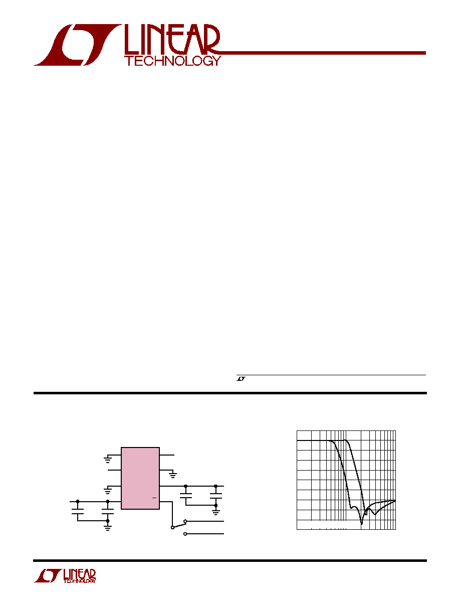
FREQUENCY (MHz)
0.1
≠ 90
GAIN (dB)
≠70
≠50
≠30
≠10
1
10
1560-1 TA02
10
≠ 80
≠ 60
≠40
≠20
0
f
CUTOFF
= 1MHz/500kHz
Frequency Response
, LTC and LT are registered trademarks of Linear Technology Corporation.
TYPICAL APPLICATIO
N
U
DESCRIPTIO
N
U
The LTC
Æ
1560-1 is a 5th order, continuous-time, lowpass
filter.
The elliptic transfer function of the LTC1560-1 was
carefully chosen to reach a compromise between selectiv-
ity, for antialiasing applications, and transient response.
The filter cutoff frequency, f
CUTOFF
, is pin selectable to
s
Antialiasing Filters
s
Smoothing or Reconstruction Filters
s
Communication Filters
APPLICATIO
N
S
U
V
IN
V
OUT
5V
(OR ≠ 5V)
0.01
µ
F
0.1
µ
F
0.1
µ
F
≠ 5V
1560-1 TA01
0.01
µ
F
≠ 5V
1MHz
5V
500kHz
GND
V
≠
V
+
GND
V
IN
1
4
3
2
8
5
6
7
V
OUT
SHDN
0.5f
C
/f
C
LTC1560-1
1MHz/500kHz Elliptic Lowpass Filter
2
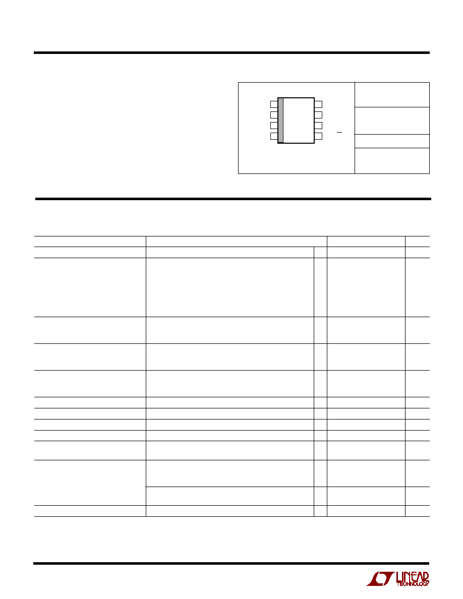
LTC1560-1
ABSOLUTE
M
AXI
M
U
M
RATINGS
W
W
W
U
PACKAGE/ORDER I
N
FOR
M
ATIO
N
W
U
U
Total Supply Voltage (V
+
to V
≠
) ............................. 12V
Power Dissipation ............................................. 400mW
Burn-In Voltage ...................................................
±
5.5V
Operating Temperature Range
LTC1560-1C ........................................... 0
∞
C to 70
∞
C
LTC1560-1I ....................................... ≠ 40
∞
C to 85
∞
C
Maximum Junction Temperature ......................... 150
∞
C
Storage Temperature Range ................. ≠ 65
∞
C to 150
∞
C
Lead Temperature (Soldering, 10 sec).................. 300
∞
C
ORDER PART
NUMBER
LTC1560-1CS8
LTC1560-1IS8
The
q
denotes specifications which apply over the full operating
temperature range.
Note 1: To properly measure high frequency characteristics of the filter, a
noninverting output buffer is recommended as shown on the demo board
connection diagram, Figure 2. A small resistor (e.g. 100
) can also be
used instead of the buffer to isolate any high capacitive load (C
L
> 10pF)
from the filter output.
Note 2: The stopband gain at 2.44MHz is guaranteed by design.
PARAMETER
CONDITIONS
MIN
TYP
MAX
UNITS
Operating Supply Voltage Range
±
4.5
±
5.0
±
5.5
V
Passband Gain (f
CUTOFF
= 1MHz)
V
IN
= 0.5V
RMS
, f
IN
= 20kHz
0.17
dB
f
IN
= 100kHz
q
≠ 0.3
0.18
0.6
dB
f
IN
= 300kHz
0.08
dB
f
IN
= 550kHz (Gain Relative to 100kHz)
q
≠ 0.35
0.05
0.3
dB
f
IN
= 850kHz (Gain Relative to 100kHz)
q
≠ 0.8
≠ 0.3
0
dB
f
IN
= 950kHz (Gain Relative to 100kHz)
q
≠ 3.0
0.6
0.5
dB
f
IN
= f
CUTOFF
= 1MHz (Gain Relative to 100kHz)
q
≠ 5.0
≠ 1.0
1.0
dB
Transition Band Gain (Note 1)
V
IN
= 0.5V
RMS
, f
IN
= 1.4MHz
q
≠ 24
≠18
dB
f
IN
= 1.9MHz
≠ 42
dB
f
IN
= 2.0MHz
≠ 51
dB
Stopband Gain (f
CUTOFF
= 1MHz) (Note 2)
f
IN
= 2.44MHz
q
≠ 70
≠ 65
dB
f
IN
= 3.0MHz
≠ 68
dB
f
IN
= 6.0MHz
≠ 66.1
dB
Passband Gain (f
CUTOFF
= 500kHz)
f
IN
= 100kHz, Pin 5 = 5V
0.14
dB
f
IN
= f
CUTOFF
= 500kHz
q
≠ 4
≠ 1.6
0.5
dB
f
IN
= 1.4MHz
≠ 45
dB
Output Voltage Swing
R
L
= 5k
q
±
1.9
±
3
V
Output DC Offset (V
OS
)
±
250
mV
Power Supply Current (I
S
)
q
22
29
mA
Power Supply Current in Shutdown Mode
Pin 7 at 5V
1
mA
Total Output Noise
V
IN
(Pin 2) Tied to Ground, f
CUTOFF
= 1MHz, BW = 2MHz
350
µ
V
RMS
V
IN
(Pin 2) Tied to Ground, f
CUTOFF
= 0.5MHz, BW = 1MHz
322
µ
V
RMS
Total Harmonic Distortion (THD)
V
IN
= 1V
RMS
, f
IN
= 200kHz, f
CUTOFF
= 1MHz, BW = 1MHz
≠ 63
dB
f
IN
= 300kHz, f
CUTOFF
= 1MHz, BW = 1MHz
≠ 61
dB
f
IN
= 1MHz, f
CUTOFF
= 1MHz, BW = 2MHz
≠ 62
dB
f
IN
= 300kHz, f
CUTOFF
= 0.5MHz, BW = 1MHz
≠ 62
dB
f
IN
= 500kHz, f
CUTOFF
= 0.5MHz, BW = 1MHz
≠ 63
dB
Input Resistance (R
IN
)
q
6
8
10
k
ELECTRICAL CHARACTERISTICS
V
S
=
±
5V, T
A
= 25
∞
C, Pin 5 = ≠ 5V (f
CUTOFF
= 1MHz), Pin 7 = 0V unless otherwise specified.
S8 PART MARKING
15601
15601I
Consult factory for Military grade parts.
T
JMAX
= 150
∞
C,
JA
= 125
∞
C/ W
1
2
3
4
8
7
6
5
TOP VIEW
V
OUT
SHDN
V
+
GND
V
IN
GND
V
≠
S8 PACKAGE
8-LEAD PLASTIC SO
0.5f
C/
f
C
3
LTC1560-1
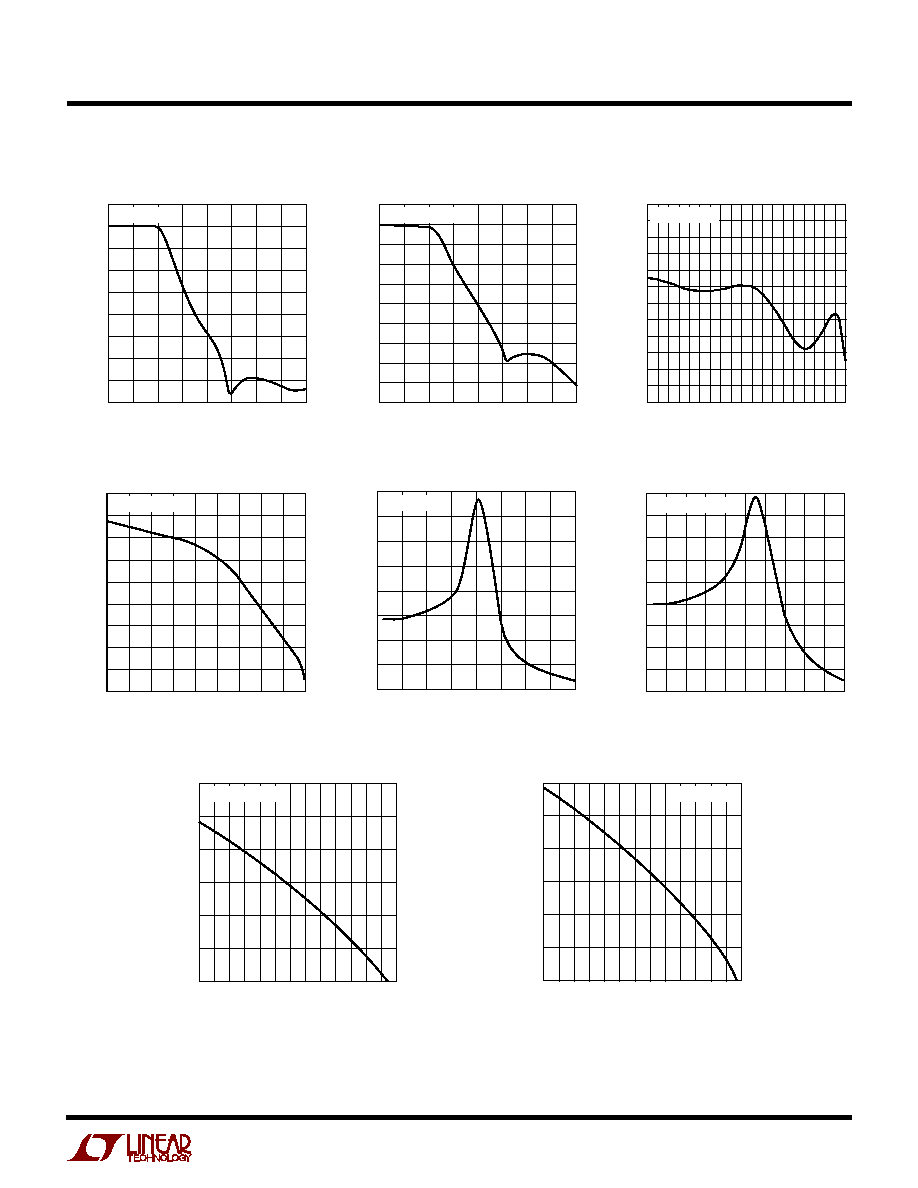
FREQUENCY (MHz)
0.1
GAIN (dB)
0
0.2
0.4
0.6
0.5
1560-1 G03
≠ 0.2
≠ 0.4
≠ 0.6
0.2 0.3 0.4
0.6 0.7 0.8 0.9 1.0
f
CUTOFF
= 1MHz
FREQUENCY (MHz)
0
GAIN (dB)
≠ 40
≠30
≠20
2.0
1560-1 G02
≠50
≠ 60
≠ 80
≠90
0.5
1.0
1.5
≠70
0
10
≠10
f
CUTOFF
= 500kHz
Frequency Response
Passband Gain
Group Delay
Passband Gain
FREQUENCY (MHz)
≠1.4
GAIN (dB)
≠1.2
≠ 0.8
≠ 0.6
≠ 0.4
0.3
0.4
0.4
1560-1 G04
≠1.0
0.2
0.1
0.5
≠ 0.2
0
0.2
f
CUTOFF
= 500kHz
FREQUENCY (MHz)
0
0
GROUP DELAY (
µ
s)
0.25
0.75
1.00
1.25
0.2
0.4 0.5 0.6 0.7 0.8 0.9 1.0
2.25
1560-1 G06
0.50
0.1
0.3
1.50
1.75
2.00
f
CUTOFF
= 500kHz
FREQUENCY (MHz)
0
GAIN (dB) ≠ 40
≠30
≠20
4
1560-1 G01
≠50
≠ 60
≠ 80
1
2
3
≠70
0
10
≠10
f
CUTOFF
= 1MHz
Frequency Response
TYPICAL PERFOR
M
A
N
CE CHARACTERISTICS
U
W
Group Delay
FREQUENCY (MHz)
0
GROUP DELAY (
µ
s)
0.8
1.2
2.0
1560-1 G05
0.4
0
0.50
1.0
1.50
0.25
0.75
1.25
1.75
1.6
0.6
1.0
0.2
1.4
f
CUTOFF
= 1MHz
Phase vs Frequency
FREQUENCY (kHz)
20
PHASE (DEG)
≠ 45
0
500
660
820
980
1560-1 G08
≠ 90
≠135
≠225
≠270
180
340
≠180
f
CUTOFF
= 1MHz
Phase vs Frequency
FREQUENCY (kHz)
20
PHASE (DEG)
≠ 45
0
45
500
420
1560-1 G07
≠ 90
≠135
≠225
260
100
180
340
≠180
f
CUTOFF
= 500kHz
4
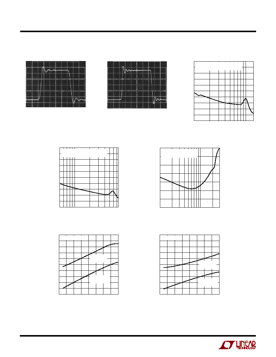
LTC1560-1
TYPICAL PERFOR
M
A
N
CE CHARACTERISTICS
U
W
FREQUENCY (MHz)
0.1
0
OUTPUT NOISE (
µ
V
RMS
)
12
24
36
48
0.5
1.5
1.0
1560-1 G11
60
6
18
30
42
54
f
CUTOFF
= 1MHz
TOTAL OUTPUT NOISE = 232
µ
V
RMS
Output Noise vs Frequency
2
µ
s/DIV
f
CUTOFF
= 0.5MHz
V
IN
= 5V
P-P
f
IN
= 50kHz
1V/DIV
1560-1 G09
Transient Response
Transient Response
2
µ
s/DIV
f
CUTOFF
= 1MHz
V
IN
= 5V
P-P
f
IN
= 50kHz
1V/DIV
1560-1 G10
Output Noise vs Frequency
Dynamic Range
INPUT VOLTAGE (V
RMS
)
≠ 90
≠ 60
≠ 70
≠ 80
≠ 20
≠ 30
≠ 40
≠ 50
1560-1 G13
THD + NOISE
0.1
3
1
f
CUTOFF
= 500kHz OR 1MHz
f
IN
= 45kHz
FREQUENCY (kHz)
50
0
OUTPUT NOISE (
µ
V
RMS
)
12
24
36
48
200
400
600
100
1560-1 G12
60
6
18
30
42
54
f
CUTOFF
= 0.5MHz
TOTAL OUTPUT NOISE = 198
µ
V
RMS
INPUT FREQUENCY (kHz)
40
THD (dB)
≠ 52
≠ 54
≠ 56
≠ 58
≠ 60
≠ 62
≠ 64
≠ 66
≠ 68
≠70
≠72
80
120
140
1560-1 G15
60
100
160 180
200
f
CUTOFF
= 1MHz
V
IN
= 1V
RMS
S/N = 72dB
V
IN
= 0.6V
RMS
S/N = 68dB
THD + Noise vs Input Frequency
THD + Noise vs Input Frequency
INPUT FREQUENCY (kHz)
40
THD (dB)
≠ 52
≠ 54
≠ 56
≠ 58
≠ 60
≠ 62
≠ 64
≠ 66
≠ 68
≠70
≠72
80
120
140
1560-1 G14
60
100
160 180
200
f
CUTOFF
= 500kHz
V
IN
= 1V
RMS
S/N = 74dB
V
IN
= 0.6V
RMS
S/N = 69.5dB
5
LTC1560-1
PI
N
FU
N
CTIO
N
S
U
U
U
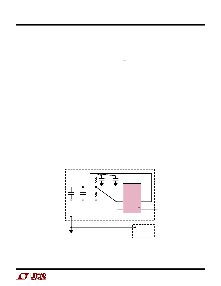
GND (Pins 1, 3): Analog Ground Pins. The quality of the
analog ground can affect the filter performance. For dual
supply operation the analog ground pin should be con-
nected to an analog ground plane surrounding the pack-
age. The analog ground plane should be connected to a
digital ground plane (if any) at a single point. For single
supply operation, the analog ground pin should be biased
at one-half the power supply across the device (see
Figure 1) and the analog ground plane should then be
connected to V
≠
(Pin 4).
V
IN
(Pin 2): The filter input is internally connected to the
inverting input of a high frequency op amp through an 8k
resistor.
V
≠
, V
+
(Pins 4, 6): Power Supply Pins. The negative and
positive power supply (Pins 4 and 6 respectively) should
be decoupled with a 0.1
µ
F capacitor in parallel with a
0.01
µ
F. Both capacitors should be types designed for
decoupling video frequencies and they should be placed
as close as possible to the power supply pins of the filter.
Parallel routing of high frequency signal paths should be
avoided; they will couple into the device's power supply
pins and cause gain inaccuracy and stopband degrada-
tion. The power supplies can be applied in any order, that
is, the positive supply can be applied before the negative
supply and vice versa. Switching power supplies are not
recommended.
0.5f
C
/f
C
(Pin 5): By tying Pin 5 high the filter cutoff
frequency is internally programmed for 500kHz. By tying
Pin 5 low the cutoff frequency will switch to 1MHz. Pin 5
should not be left floating. The logic threshold of Pin 5 is
approximately 0.4 times the total power supply across the
device.
SHDN (Pin 7): Shutdown. Under normal operating condi-
tions, Pin 7 should be shorted either to the analog ground
(Pin 1) or to V
≠
(Pin 4). If Pin 7 is pulled high to V
+
, the filter
operation will stop and the IC will be placed in a power
saving mode. The power supply current will then be
reduced to 1mA. For a
±
5V supply, the logic threshold of
Pin 7 is 2.5V. Pin 7 is internally connected to the analog
ground pin via a 50k resistor.
V
OUT
(Pin 8): The filter output pin can sink or source 1mA.
The total harmonic distortion of the filter will degrade
when driving coaxial cables or loads less than 10k without
an output buffer.
Figure 1. Connections for Single Supply Operation
V
+
1560-1 F01
V
IN
V
OUT
0.01
µ
F
0.1
µ
F
0.01
µ
F
1
µ
F
10k
10k
GND OR V
+
ANALOG GROUND PLANE
SYSTEM GROUND
DIGITAL GROUND
PLANE
GND
V
≠
V
+
GND
V
IN
1
4
3
2
8
5
6
7
V
OUT
SHDN
0.5f
C
/f
C
LTC1560-1
6
LTC1560-1
APPLICATIO
N
S I
N
FOR
M
ATIO
N
W
U
U
U
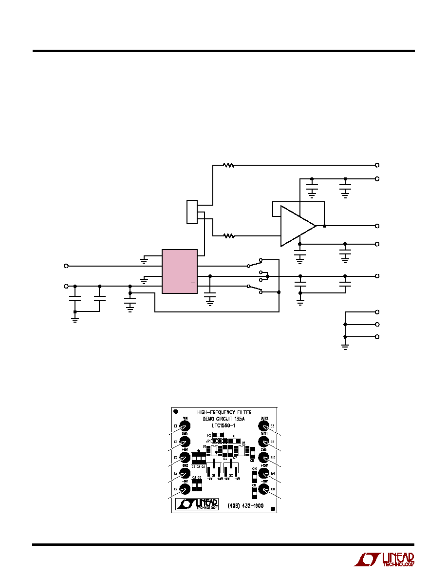
The performance of the LTC1560-1 can be easily evaluated
by using demo board 135A which can be obtained through
LTC marketing. Figure 2 shows the circuit connection of
the LTC1560-1 in demo board 135A. The filter cutoff
frequency can be switched via S2 and the power savings
mode can also be activated via S1. The output of the filter
is buffered by U2, an LT
Æ
1360 op amp. The buffering can
be bypassed by using jumper JP1. Figure 3 shows the
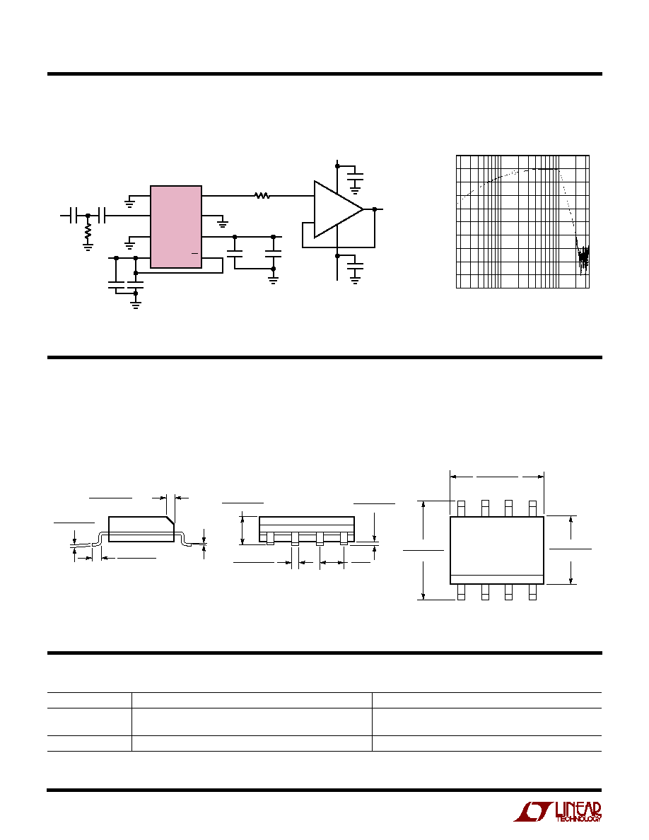
demo board layout.
Figure 3. Demo Board 135A Layout
UNBUFFERED OUTPUT
FILTER INPUT
GROUND
+ 5V FILTER SUPPLY
GROUND
≠ 5V FILTER SUPPLY
BUFFERED OUTPUT
GROUND
+15V BUFFER SUPPLY
≠ 15V BUFFER SUPPLY
1560-1 F03
1
2
3
4
8
7
6
5
U1
LTC1560-1
JP1
JUMPER
R1
1k
2
7
4
3
6
V
OUT
SHDN
V
+
0.5f
C
/f
C
GND
V
IN
GND
V
≠
C1
0.01
µ
F
C9
0.01
µ
F
C10
1
µ
F
25V
Y5V
C8
1
µ
F
25V
Y5V
C6
1
µ
F
16V
X7R
C5
0.22
µ
F
C4
0.01
µ
F
C2
0.22
µ
F
E2
TP
≠ 5V
C3
1
µ
F
16V
X7R
S1
GS01MSCKE
S2
GS01MSCKE
E1
TP
V
IN
3
2
1
R2
332
≠
+
U2
LT1360CS8
C7
0.01
µ
F
E10
TP
GND
E9
TP
GND
E8
TP
GND
E7
TP
5V
1560-1 F02
E6
TP
≠ 15V
E5
TP
OUT1
E4
TP
15V
E3
TP
OUT2
Figure 2. Demo Board 135A Connection Diagram

7
LTC1560-1
Information furnished by Linear Technology Corporation is believed to be accurate and reliable.
However, no responsibility is assumed for its use. Linear Technology Corporation makes no represen-
tation that the interconnection of its circuits as described herein will not infringe on existing patent rights.
TYPICAL APPLICATIO
N
S
N
U
Augmenting the LTC1560-1 for Improved Delay Flatness
Gain vs Frequency
1MHz Lowpass Filter Cascaded with a 30kHz 3rd Order Highpass Filter
FREQUENCY (kHz)
0.1
≠ 60
GAIN (dB)
≠ 50
≠ 40
≠ 30
≠ 20
≠10
1
10
100
1000
10,000
1560-1 TA10
≠ 70
≠ 80
≠ 90
≠100
≠110
0
10
≠
+
≠
+
≠ 5V
5V
0.1
µ
F
0.1
µ
F
2.61k
560pF
560pF
560pF
3
1k
23.7k
2
4
8
1/2 LT1364
1
6
5
1/2 LT1364
7
0.1
µ
F
39pF
(OR ≠ 5V)
0.01
µ
F
0.1
µ
F
0.01
µ
F
V
IN
1560-1 TA09
560pF
GND
V
≠
V
+
GND
V
IN
1
4
3
2
8
5
6
7
V
OUT
SHDN
0.5f
C
/f
C
LTC1560-1
≠
+
≠
+
5V
2
6.49k
6.65k
49.9
22pF
0.1
µ
F
0.1
µ
F
22pF
9.75k
20k
40.2k
3
V
OUT
1/2 LT1364
1
6
5
4
8
5V
1/2 LT1364
≠ 5V
7
0.1
µ
F
(OR ≠ 5V)
0.01
µ
F
0.01
µ
F
0.1
µ
F
V
IN
≠5V
1560-1 TA05
GND
V
≠
V
+
GND
V
IN
1
4
3
2
8
5
6
7
V
OUT
SHDN
0.5f
C
/f
C
LTC1560-1
2-Level Eye Diagram of the Equalized Filter
2Mbps/s
1560-1 TA06
8
LTC1560-1
Linear Technology Corporation
1630 McCarthy Blvd., Milpitas, CA 95035-7417
q
(408) 432-1900
FAX: (408) 434-0507
q
TELEX: 499-3977
q
www.linear-tech.com
©
LINEAR TECHNOLOGY CORPORATION 1997
15601f LT/GP 1197 4K ∑ PRINTED IN USA
TYPICAL APPLICATIO
N
U
PACKAGE DESCRIPTIO
N
U
Dimensions in inches (millimeters) unless otherwise noted.
RELATED PARTS
PART NUMBER
DESCRIPTION
COMMENTS
LT1360/LT1361/
50MHz, 800V/
µ
s Op Amp(s)
Single/Dual/Quad C-Load
TM
Op Amps
LT1362
LTC1562
Active RC Quad Universal Filter
Very Low Noise, Low Distortion
C-Load is a trademark of Linear Technology Corporation
S8 Package
8-Lead Plastic Small Outline (Narrow 0.150)
(LTC DWG # 05-08-1610)
0.016 ≠ 0.050
0.406 ≠ 1.270
0.010 ≠ 0.020
(0.254 ≠ 0.508)
◊
45
∞
0
∞
≠ 8
∞
TYP
0.008 ≠ 0.010
(0.203 ≠ 0.254)
SO8 0695
0.053 ≠ 0.069
(1.346 ≠ 1.752)
0.014 ≠ 0.019
(0.355 ≠ 0.483)
0.004 ≠ 0.010
(0.101 ≠ 0.254)
0.050
(1.270)
BSC
1
2
3
4
0.150 ≠ 0.157**
(3.810 ≠ 3.988)
8
7
6
5
0.189 ≠ 0.197*
(4.801 ≠ 5.004)
0.228 ≠ 0.244
(5.791 ≠ 6.197)
DIMENSION DOES NOT INCLUDE MOLD FLASH. MOLD FLASH
SHALL NOT EXCEED 0.006" (0.152mm) PER SIDE
DIMENSION DOES NOT INCLUDE INTERLEAD FLASH. INTERLEAD
FLASH SHALL NOT EXCEED 0.010" (0.254mm) PER SIDE
*
**
≠
+
≠15V
15V
0.1
µ
F
0.1
µ
F
5V
3
1k
2
4
V
OUT
7
LT1360
8
0.1
µ
F
(OR ≠ 5V)
0.01
µ
F
0.01
µ
F
8.1k
0.1
µ
F
V
IN
300pF
≠5V
1560-1 TA07
300pF
GND
V
≠
V
+
GND
V
IN
1
4
3
2
8
5
6
7
V
OUT
SHDN
0.5f
C
/f
C
LTC1560-1
FREQUENCY (kHz)
≠90
≠70
≠80
≠60
≠40
≠50
0
≠10
≠20
≠30
10
GAIN (dB)
10000
1560-1 TA08
20
100
1000
A Simple Highpass/Lowpass Filter
Measured Frequency Response