 | –≠–ª–µ–∫—Ç—Ä–æ–Ω–Ω—ã–π –∫–æ–º–ø–æ–Ω–µ–Ω—Ç: LTC1569I | –°–∫–∞—á–∞—Ç—å:  PDF PDF  ZIP ZIP |
1
LTC1569-7
TYPICAL APPLICATIO
N
U
DESCRIPTIO
U
APPLICATIO S
U
FEATURES
s
One External R Sets Cutoff Frequency
s
Root Raised Cosine Response
s
Up to 300kHz Cutoff on a Single 5V Supply
s
Up to 150kHz Cutoff on a Single 3V Supply
s
10th Order, Linear Phase Filter in an SO-8
s
DC Accurate, V
OS(MAX)
= 5mV
s
Low Power Modes
s
Differential or Single-Ended Inputs
s
80dB CMRR (DC)
s
80dB Signal-to-Noise Ratio, V
S
= 5V
s
Operates from 3V to
±
5V Supplies
The LTC
Æ
1569-7 is a 10th order lowpass filter featuring
linear phase and a root raised cosine amplitude response.
The high selectivity of the LTC1569-7 combined with its
linear phase in the passband makes it suitable for filtering
both in data communications and data acquisition sytems.
s
Data Communication Filters for 3V Operation
s
Linear Phase and Phase Matched Filters for I/Q
Signal Processing
s
Pin Programmable Cutoff Frequency Lowpass Filters
Furthermore, its root raised cosine response offers the
optimum pulse shaping for PAM data communications.
The filter attenuation is 50dB at 1.5 ∑ f
CUTOFF
, 60dB at 2 ∑
f
CUTOFF
, and in excess of 80dB at 6 ∑ f
CUTOFF
. DC-accuracy-
sensitive applications benefit from the 5mV maximum DC
offset.
The LTC1569-7 is the first sampled data filter which does
not require an external clock yet its cutoff frequency can be
set with a single external resistor with a typical accuracy
of 3.5% or better. The external resistor programs an
internal oscillator whose frequency is divided by either 1,
4 or 16 prior to being applied to the filter network. Pin 5
determines the divider setting. Thus, up to three cutoff
frequencies can be obtained for each external resistor
value. Using various resistor values and divider settings,
the cutoff frequency can be programmed over a range of
seven octaves. Alternatively, the cutoff frequency can be
set with an external clock and the clock-to-cutoff fre-
quency ratio is 32:1. The ratio of the internal sampling rate
to the filter cutoff frequency is 64:1.
The LTC1569-7 is fully tested for a cutoff frequency of
256kHz/128kHz with single 5V/3V supply although up to
300kHz cutoff frequencies can be obtained.
The LTC1569-7 features power savings modes and it is
available in an SO-8 surface mount package.
, LTC and LT are registered trademarks of Linear Technology Corporation.
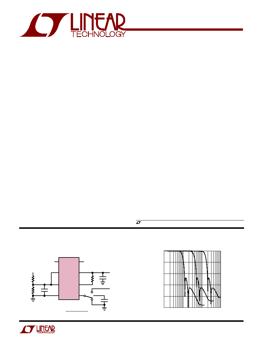
Frequency Response, f
CUTOFF
= 128kHz/32kHz/8kHz
Single 3V Supply, 128kHz/32kHz/8kHz Lowpass Filter
Linear Phase, DC Accurate,
Tunable, 10th Order Lowpass Filter
FREQUENCY (kHz)
1
GAIN (dB)
0
≠20
≠40
≠60
≠80
≠100
10
100
1000
1569-7 TA01a
1
8
2
7
3
6
4
5
1
µ
F
3V
1/4
1/16
1/1
3V
R
EXT
= 10k
100pF
1
µ
F
2k
3.48k
3V
LTC1569-7
EASY TO SET f
CUTOFF
:
f
CUTOFF
=
128kHz (10k/R
EXT
)
1, 4 OR 16
1569-7 TA01
IN
+
IN
≠
GND
V
≠
OUT
V
IN
V
OUT
V
+
R
X
DIV/CLK
2
LTC1569-7
PARAMETER
CONDITIONS
MIN
TYP
MAX
UNITS
Filter Gain
V
S
= 5V, f
CLK
= 8.192MHz,
f
IN
= 5120Hz = 0.02 ∑ f
CUTOFF
q
≠ 0.10
0.00
0.10
dB
f
CUTOFF
= 256kHz, V
IN
= 2.5V
P-P
,
f
IN
= 51.2kHz = 0.2 ∑ f
CUTOFF
q
≠ 0.25
≠ 0.15
≠ 0.05
dB
R
EXT
= 5k, Pin 5 Shorted to Pin 4
f
IN
= 128kHz = 0.5 ∑ f
CUTOFF
q
≠ 0.50
≠ 0.41
≠ 0.25
dB
f
IN
= 204.8kHz = 0.8 ∑ f
CUTOFF
q
≠ 1.1
≠ 0.65
≠ 0.40
dB
f
IN
= 256kHz = f
CUTOFF
, LTC1569C
q
≠ 5.7
≠ 3.8
≠ 2.3
dB
f
IN
= 256kHz = f
CUTOFF
, LTC1569I
q
≠ 6.2
≠ 3.8
≠ 2.0
dB
f
IN
= 384kHz = 1.5 ∑ f
CUTOFF
q
≠ 58
≠ 48
dB
f
IN
= 512kHz = 2 ∑ f
CUTOFF
q
≠ 62
≠ 54
dB
f
IN
= 768kHz = 3 ∑ f
CUTOFF
q
≠ 67
≠ 64
dB
V
S
= 2.7V, f
CLK
= 1MHz,
f
IN
= 625Hz = 0.02 ∑ f
CUTOFF
q
≠ 0.08
0.00
0.12
dB
f
CUTOFF
= 31.25kHz, V
IN
= 1V
P-P
,
f
IN
= 6.25kHz = 0.2 ∑ f
CUTOFF
q
≠ 0.25
≠ 0.15
≠ 0.05
dB
Pin 6 Shorted to Pin 4, External Clock
f
IN
= 15.625kHz = 0.5 ∑ f
CUTOFF
q
≠ 0.50
≠ 0.40
≠ 0.30
dB
f
IN
= 25kHz = 0.8 ∑ f
CUTOFF
q
≠ 0.75
≠ 0.65
≠ 0.50
dB
f
IN
= 31.25kHz = f
CUTOFF
q
≠ 3.3
≠ 3.15
≠ 3.0
dB
f
IN
= 46.875kHz = 1.5 ∑ f
CUTOFF
q
≠ 57
≠ 52
dB
f
IN
= 62.5kHz = 2 ∑ f
CUTOFF
q
≠ 60
≠ 54
dB
f
IN
= 93.75kHz = 3 ∑ f
CUTOFF
q
≠ 66
≠ 58
dB
Filter Phase
V
S
= 2.7V, f
CLK
= 4MHz,
f
IN
= 2500Hz = 0.02 ∑ f
CUTOFF
≠11
Deg
f
CUTOFF
= 125kHz, Pin 6 Shorted to
f
IN
= 25kHz = 0.2 ∑ f
CUTOFF
q
≠ 114
≠112
≠110
Deg
Pin 4, External Clock
f
IN
= 62.5kHz = 0.5 ∑ f
CUTOFF
q
78
80
82
Deg
f
IN
= 100kHz = 0.8 ∑ f
CUTOFF
q
≠ 85
≠ 83
≠ 81
Deg
f
IN
= 125kHz = f
CUTOFF
q
155
158
161
Deg
f
IN
= 187.5kHz = 1.5 ∑ f
CUTOFF
≠ 95
Deg
Filter Cutoff Accuracy
R
EXT
= 10.24k from Pin 6 to Pin 7,
125kHz
±
1%
when Self-Clocked
V
S
= 3V, Pin 5 Shorted to Pin 4
Filter Output DC Swing
V
S
= 3V, Pin 3 = 1.11V
2.1
V
P-P
q
1.9
V
P-P
V
S
= 5V, Pin 3 = 2V
3.9
V
P-P
q
3.7
V
P-P
V
S
=
±
5V
8.6
V
P-P
LTC1569C
q
8.4
V
P-P
LTC1569I
q
8.0
V
P-P
A
U
G
W
A
W
U
W
A
R
BSOLUTE
XI
TI
S
ORDER PART
NUMBER
W
U
U
PACKAGE/ORDER I FOR ATIO
(Note 1)
Total Supply Voltage ................................................ 11V
Power Dissipation .............................................. 500mW
Operating Temperature
LTC1569C ............................................... 0
∞
C to 70
∞
C
LTC1569I ............................................ ≠ 40
∞
C to 85
∞
C
Storage Temperature ............................ ≠ 65
∞
C to 150
∞
C
Lead Temperature (Soldering, 10 sec).................. 300
∞
C
The
q
denotes the specifications which apply over the full operating temperature range, otherwise specifications are at T
A
= 25
∞
C.
V
S
= 3V (V
+
= 3V, V
≠
= 0V), f
CUTOFF
= 128kHz, R
LOAD
= 10k unless otherwise specified.
ELECTRICAL C
C
HARA TERISTICS
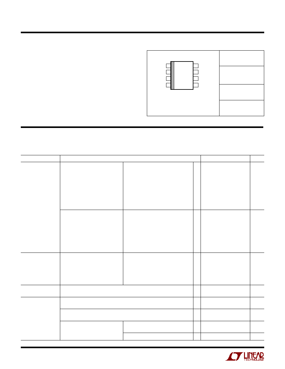
LTC1569CS8-7
LTC1569IS8-7
S8 PART
MARKING
Consult factory for Military grade parts.
T
JMAX
= 125
∞
C,
JA
= 80
∞
C/W (Note 6)
15697
1569I7
1
2
3
4
8
7
6
5
TOP VIEW
OUT
V
+
R
X
DIV/CLK
IN
+
IN
≠
GND
V
≠
S8 PACKAGE
8-LEAD PLASTIC SO
3
LTC1569-7
Output DC Offset
R
EXT
= 10k, Pin 5 Shorted to Pin 4
V
S
= 3V
±
2
±
5
mV
(Note 2)
V
S
= 5V
±
6
±
12
mV
V
S
=
±
5V
±
15
mV
Output DC Offset Drift
R
EXT
= 10k, Pin 5 Shorted to Pin 4
V
S
= 3V
≠ 25
µ
V/
∞
C
V
S
= 5V
≠ 25
µ
V/
∞
C
V
S
=
±
5V
±
25
µ
V/
∞
C
Clock Pin Logic Thresholds
V
S
= 3V
Min Logical "1"
2.6
V
when Clocked Externally
Max Logical "0"
0.5
V
V
S
= 5V
Min Logical "1"
4.0
V
Max Logical "0"
0.5
V
V
S
=
±
5V
Min Logical "1"
4.0
V
Max Logical "0"
0.5
V
Power Supply Current
f
CLK
= 1.028MHz (10k from Pin 6 to Pin 7,
V
S
= 3V
6
8
mA
(Note 3)
Pin 5 Open,
˜
4), f
CUTOFF
= 32kHz
q
9
mA
V
S
= 5V
7
9
mA
q
10
mA
V
S
= 10V
9
13
mA
q
14
mA
f
CLK
= 4.096MHz (10k from Pin 6 to Pin 7,
V
S
= 3V
9.5
mA
Pin 5 Shorted to Pin 4,
˜
1), f
CUTOFF
= 128kHz
q
14
mA
f
CLK
= 8.192MHz (5k from Pin 6 to Pin 7,
V
S
= 5V
20
mA
Pin 5 Shorted to Pin 4,
˜
1), f
CUTOFF
= 256kHz
q
30
mA
V
S
= 10V
27
mA
q
37
mA
Power Supply Voltage where
Pin 5 Shorted to Pin 4, Note 3
q
3.7
4.2
4.6
V
Low Power Mode is Enabled
Clock Feedthrough
R
EXT
= 10k, Pin 5 Open
0.4
mV
RMS
Wideband Noise
Noise BW = DC to 2 ∑ f
CUTOFF
125
µ
V
RMS
THD
f
IN
= 10kHz, 1.5V
P-P
74
dB
Clock-to-Cutoff
32
Frequency Ratio
Max Clock Frequency
V
S
= 3V
5
MHz
(Note 4)
V
S
= 5V
9.6
MHz
V
S
=
±
5V
13
MHz
Min Clock Frequency
3V to
±
5V, T
A
< 85
∞
C
3
kHz
(Note 5)
Input Frequency Range
Aliased Components <≠65dB
0.9 ∑ f
CLK
Hz
The
q
denotes the specifications which apply over the full operating temperature range, otherwise specifications are at T
A
= 25
∞
C.
V
S
= 3V (V
+
= 3V, V
≠
= 0V), f
CLK
= 4.096MHz, f
CUTOFF
= 128kHz, R
LOAD
= 10k unless otherwise specified.
ELECTRICAL C
C
HARA TERISTICS
PARAMETER
CONDITIONS
MIN
TYP
MAX
UNITS
Note 1: Absolute maximum ratings are those values beyond which the life
of a device may be impaired.
Note 2: DC offset is measured with respect to Pin 3.
Note 3: There are several operating modes which reduce the supply
current. For V
S
< 4V, the current is reduced by 50%. If the internal
oscillator is used as the clock source and the divide-by-4 or divide-by-16
mode is enabled, the supply current is reduced by 60% independent of the
value of V
S
.
Note 4: The maximum clock frequency is arbitrarily defined as the
frequency at which the filter AC response exhibits >1dB of gain peaking.
Note 5: The minimum clock frequency is arbitrarily defined as the frequecy
at which the filter DC offset changes by more than 5mV.
Note 6: Thermal resistance varies depending upon the amount of PC board
metal attached to the device.
JA
is specified for a 2500mm
2
test board
covered with 2oz copper on both sides.
4
LTC1569-7
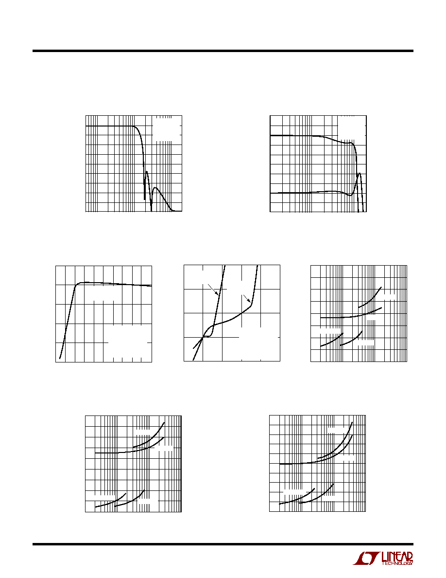
TYPICAL PERFOR A CE CHARACTERISTICS
U
W
THD vs Input Voltage
THD vs Input Frequency
INPUT VOLTAGE (V
P-P
)
0
1
2
3
4
5
THD (dB)
1569-7 G02
≠50
≠60
≠70
≠80
≠90
f
IN
= 10kHz
f
CUTOFF
= 128kHz
IN
+
TO OUT
R
EXT
= 10k
PIN 5 AT V
≠
V
S
= 5V
PIN 3 = 2V
V
S
= 3V
PIN 3 = 1.11V
INPUT FREQUENCY (kHz)
0
20
10
30
50
70
90
40
60
80
100
THD (dB)
1569-7 G01
≠68
≠70
≠72
≠74
≠76
≠78
V
IN
= 1.5V
P-P
f
CUTOFF
= 128kHz
IN
+
TO OUT
R
EXT
= 10k
PIN 5 AT V
≠
V
S
= 5V
PIN 3 = 2V
FREQUENCY (kHz)
5
LOG MAG (10dB/DIV)
10
≠90
10
100
1000
1569-7 G03
V
S
= 3V
f
C
= 128kHz
R
EXT
= 10k
PIN 5 AT V
≠
FREQUENCY (kHz)
1
GAIN (dB)
DELAY (
µ
s)
1
0
≠1
≠2
≠3
≠4
20
19
18
17
16
15
14
13
12
11
10
10
100
1569-7 G04
V
S
= 3V
f
C
= 128kHz
R
EXT
= 10k
PIN 5 AT V
≠
Gain vs Frequency
Passband Gain and Group Delay
vs Frequency
f
CUTOFF
(kHz)
1
I
SUPPLY
(mA)
10
100
1000
1569-7 G05
12
11
10
9
8
7
6
5
4
DIV-BY-16
DIV-BY-4
DIV-BY-1
EXT CLK
f
CUTOFF
(kHz)
1
I
SUPPLY
(mA)
10
100
1000
1569-7 G06
23
21
19
17
15
13
11
9
7
5
DIV-BY-16
DIV-BY-4
DIV-BY-1
EXT CLK
5V Supply Current
3V Supply Current
f
CUTOFF
(kHz)
1
I
SUPPLY
(mA)
10
100
1000
1569-7 G07
35
32
29
26
23
20
17
14
11
8
5
DIV-BY-16
DIV-BY-4
DIV-BY-1
EXT CLK
±
5V Supply Current
5
LTC1569-7
PI
N
FU
N
CTIO
N
S
U
U
U
IN
+
/IN
≠
(Pins 1, 2): Signals can be applied to either or
both input pins. The DC gain from IN
+
(Pin 1) to OUT
(Pin 8) is 1.0, and the DC gain from Pin 2 to Pin 8 is ≠1. The
input range, input resistance and output range are de-
scribed in the Applications Information section. Input
voltages which exceed the power supply voltages should
be avoided. Transients will not cause latchup if the current
into/out of the input pins is limited to 20mA.
GND (Pin 3): The GND pin is the reference voltage for the
filter and should be externally biased to 2V (1.11V) to
maximize the dynamic range of the filter in applications
using a single 5V (3V) supply. For single supply operation,
the GND pin should be bypassed with a quality 1
µ
F
ceramic capacitor to V
≠
(Pin 4). The impedance of the
circuit biasing the GND pin should be less than 2k
as the
GND pin generates a small amount of AC and DC current.
For dual supply operation, connect Pin 3 to a high quality
DC ground. A ground plane should be used. A poor ground
will increase DC offset, clock feedthrough, noise and
distortion.
V
≠
/V
+
(Pins 4, 7): For 3V, 5V and
±
5V applications a
quality 1
µ
F ceramic bypass capacitor is required from V
+
(Pin 7) to V
≠
(Pin 4) to provide the transient energy for the
internal clock drivers. The bypass should be as close as
possible to the IC. In dual supply applications (Pin 3 is
grounded), an additional 0.1
µ
F bypass from V
+
(Pin 7) to
GND (Pin 3) and V
≠
(Pin 4) to GND (Pin 3) is recom-
mended.
The maximum voltage difference between GND (Pin 3) and
V
+
(Pin 7) should not exceed 5.5V.
DIV/CLK (Pin 5): DIV/CLK serves two functions. When the
internal oscillator is enabled, DIV/CLK can be used to
engage an internal divider. The internal divider is set to 1:1
when DIV/CLK is shorted to V
≠
(Pin 4). The internal divider
is set to 4:1 when DIV/CLK is allowed to float (a 100pF
bypass to V
≠
is recommended). The internal divider is set
to 16:1 when DIV/CLK is shorted to V
+
(Pin 7). In the
divide-by-4 and divide-by-16 modes the power supply
current is reduced by typically 60%.
When the internal oscillator is disabled (R
X
shorted
to V
≠
) DIV/CLK becomes an input pin for applying an
external clock signal. For proper filter operation, the clock
waveform should be a squarewave with a duty cycle as
close as possible to 50% and CMOS voltages levels (see
Electrical Characteristics section for voltage levels). DIV/
CLK pin voltages which exceed the power supply voltages
should be avoided. Transients will not cause latchup if the
fault current into/out of the DIV/CLK pin is limited to 40mA.
R
X
(Pin 6): Connecting an external resistor between the R
X
pin and V
+
(Pin 7) enables the internal oscillator. The value
of the resistor determines the frequency of oscillation. The
maximum recommended resistor value is 40k and the
minimum is 3.8k/8k (single 5V/3V supply). The internal
oscillator is disabled by shorting the R
X
pin to V
≠
(Pin 4).
(Please refer to the Applications Information section.)
OUT (Pin 8): Filter Output. This pin can drive 10k
and/or
40pF loads. For larger capacitive loads, an external 100
series resistor is recommended. The output pin can ex-
ceed the power supply voltages by up to
±
2V without
latchup.
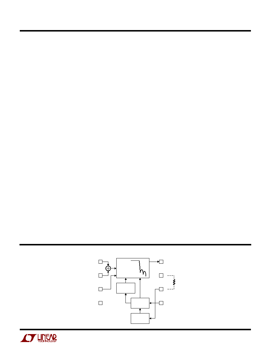
BLOCK DIAGRA
W
10TH ORDER
LINEAR PHASE
FILTER NETWORK
POWER
CONTROL
DIVIDER/
BUFFER
R
EXT
PRECISION
OSCILLATOR
5
6
7
8
4
3
2
1
OUT
V
+
R
X
DIV/CLK
IN
+
IN
≠
GND
V
≠
1569-7 BD