1
LTC1574
LTC1574-3.3/LTC1574-5
High Efficiency Step-Down
DC/DC Converters
with Internal Schottky Diode
The LTC
Æ
1574 is a family of easy-to-use current mode
DC/DC converters ideally suited for 9V to 5V, 5V to 3.3V
and inverting operation. With an internal 0.9
switch (at
a supply voltage of 12V) and a low forward drop Schottky
diode (0.450V typ at 200mA, T
A
= 25
∞
C), the LTC1574
requires only three external components to construct a
complete high efficiency DC/DC converter.
Under no load condition, the LTC1574 draws only 130
µ
A.
In shutdown, it draws a mere 2
µ
A making this converter
ideal for battery-powered applications. In dropout, the
internal P-channel MOSFET switch is turned on continu-
ously allowing the user to maximize the life of the battery
source.
The maximum inductor current of the LTC1574 family is
pin selectable to either 340mA or 600mA, optimizing
efficiency for a wide range of applications. Operation up to
200kHz permits the use of small surface mount inductors
and capacitors.
For applications requiring higher output current or ultra-
high efficiency, see the LTC1148 or LTC1265 data sheets.
For detailed applications information, see the LTC1174
data sheet.
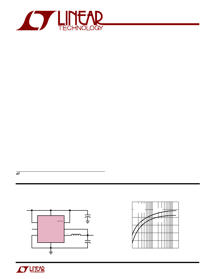
High Efficiency Step-Down Converter
LTC1574-5 Efficiency
s
Inverting Converters
s
Step-Down Converters
s
Memory Backup Supply
s
Portable Instruments
s
Battery-Powered Equipment
s
Distributed Power Systems
s
High Efficiency: Up to 94%
s
Usable in Noise-Sensitive Products
s
Peak Inductor Current Independent of Inductor Value
s
Short-Circuit Protection
s
Internal Low Forward Drop Schottky Diode
s
Only Three External Components Required
s
Wide V
IN
Range: 4V to 18.5V (Absolute Maximum)
s
Low Dropout Operation
s
Low-Battery Detector
s
Pin Selectable Current Limit
s
Internal 0.9
Power Switch: V
IN
< 11V
s
Standby Current: 130
µ
A
s
Active Low Micropower Shutdown
FEATURES
DESCRIPTIO
U
APPLICATIO S
U
TYPICAL APPLICATIO
U
and LTC are registered trademarks and LT is a trademark of Linear Technology Corporation.
V
IN
100
µ
H
22
µ
F*
35V
100
µ
F*
10V
1574 TA01
5V
175mA
5
2, 4, 13, 15
7
10
3, 14
12
11
6
V
IN
5.5V to
16V
GND
LTC1574-5
LB
IN
LB
OUT
I
PGM
SHDN
V
OUT
SW
* AVX TPSD226K035
** AVX TPSD107K010
COILTRONICS CTX100-4
+
+
LOAD CURRENT (mA)
1
EFFICIENCY (%)
100
95
90
85
80
75
70
10
100
1574 TA02
200
V
IN
= 6V
V
IN
= 9V
L = 100
µ
H
V
OUT
= 5V
I
PGM
= 0V
2
LTC1574
LTC1574-3.3/LTC1574-5
ORDER PART
NUMBER
LTC1574CS
LTC1574CS-3.3
LTC1574CS-5
Consult factory for Industrial and Military grade parts.
(Note 1)
(Voltage Referred to GND Pin)
Input Supply Voltage (Pin 5) ................. ≠ 0.3V to 18.5V
Switch Current (Pin 3, 14) ........................................ 1A
Switch Voltage (Pin 3, 14) .......................... V
IN
≠ 18.5V
Operating Temperature Range .................... 0
∞
C to 70
∞
C
Junction Temperature (Note 2) ............................ 125
∞
C
Storage Temperature Range ................. ≠ 65
∞
C to 150
∞
C
Lead Temperature (Soldering, 10 sec).................. 300
∞
C
SYMBOL PARAMETER
CONDITIONS
MIN
TYP
MAX
UNITS
I
FB
Feedback Current into Pin 10
LTC1574
1
µ
A
V
FB
Feedback Voltage
LTC1574
q
1.20
1.25
1.30
V
V
OUT
Regulated Output Voltage
LTC1574-3.3
q
3.14
3.30
3.46
V
LTC1574-5
q
4.75
5.00
5.25
V
V
OUT
Output Voltage Line
V
IN
= 6V to 12V, I
LOAD
= 100mA, I
PGM
= V
IN
(Note 3)
10
70
mV
Regulation
Output Voltage Load
LTC1574-3.3 (Note 3)
20mA < I
LOAD
< 175mA, I
PGM
= 0V
≠ 5
≠ 70
mV
Regulation
20mA < I
LOAD
< 400mA, I
PGM
= V
IN
≠ 45
≠ 70
mV
LTC1574-5 (Note 3)
20mA < I
LOAD
< 175mA, I
PGM
= 0V
≠ 5
≠ 70
mV
20mA < I
LOAD
< 400mA, I
PGM
= V
IN
≠ 50
≠ 70
mV
I
Q
Input DC Supply Current (Note 4)
Active Mode
4V < V
IN
< 16V, I
PGM
= 0V
450
600
µ
A
Sleep Mode
4V < V
IN
< 16V
130
180
µ
A
Shutdown (Note 5)
SHDN = 0V, 4V < V
IN
< 16V
2
25
µ
A
V
LBTRIP
Low-Battery Trip Point
1.25
1.4
V
I
LBIN
Current into Pin 12
0.5
µ
A
I
LBOUT
Current Sunk by Pin 11
V
LBOUT
= 0.4V, V
LBIN
= 0V
0.5
1.0
1.5
mA
V
LBOUT
= 5V, V
LBIN
= 10V
1.0
µ
A
V
HYST
Comparator Hysteresis
7.5
15
30
mV
I
PEAK
Current Limit
I
PGM
= V
IN
, V
OUT
= 0V
q
0.54
0.60
0.83
A
I
PGM
= 0V, V
OUT
= 0V
q
0.27
0.34
0.53
A
R
ON
ON Resistance of Switch
q
0.9
1.55
t
OFF
Switch Off Time
V
OUT
at Regulated Value
3
4
5
µ
s
V
IH
SHDN Pin High
Minimum Voltage at Pin 7 for Device to Be Active
1.2
V
V
IL
SHDN Pin Low
Maximum Voltage at Pin 7 for Device to Be in Shutdown
0.75
V
ABSOLUTE AXI U RATI GS
W
W
W
U
PACKAGE/ORDER I FOR ATIO
U
U
W
TOP VIEW
S PACKAGE
16-LEAD PLASTIC SO
*ADJUSTABLE OUTPUT VERSION
T
JMAX
= 125
∞
C,
JA
= 110
∞
C/W
1
2
3
4
5
6
7
8
16
15
14
13
12
11
10
9
NC
GND
SW
GND
V
IN
I
PGM
SHDN
NC
NC
GND
SW
GND
LB
IN
LB
OUT
V
OUT
(V
FB
*)
NC
ELECTRICAL CHARACTERISTICS
The
q
denotes specifications which apply over the full operating
temperature range, otherwise specifications are at T
A
= 25
∞
C. V
IN
= 9V, SHDN = V
IN
, I
PGM
= 0V, unless otherwise specified.
3
LTC1574
LTC1574-3.3/LTC1574-5
The
q
denotes specifications which apply over the full operating
temperature range, otherwise specifications are at T
A
= 25
∞
C. V
IN
= 9V, SHDN = V
IN
, I
PGM
= 0V, unless otherwise specified.
SYMBOL PARAMETER
CONDITIONS
MIN
TYP
MAX
UNITS
I
IH
SHDN Pin Input Current
SHDN = 16V
2
µ
A
I
IL
SHDN Pin Input Current
0
SHDN
0.8V
0.5
µ
A
V
F
Schottky Diode Forward Voltage
Forward Current = 200mA
0.450
0.570
V
I
R
Schottky Reverse Current
Reverse Voltage = 5V
10
25
µ
A
Reverse Voltage = 18.5V
100
250
µ
A
Note 1: Absolute Maximum Ratings are those values beyond which the life
of a device may be impaired.
Note 2: T
J
is calculated from the ambient temperature T
A
and power
dissipation P
D
according to the following formulas:
T
J
= T
A
+ (P
D
∑ 110
∞
C/W)
Note 3: Guaranteed by design.
Note 4: Does not include Schottky reverse current. Dynamic supply
current is higher due to the gate charge being delivered at the switching
frequency.
Note 5: Current into Pin 5 only, measured without electrolytic input
capacitor.
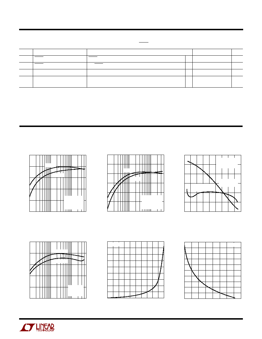
TYPICAL PERFOR
M
A
N
CE CHARACTERISTICS
U
W
Efficiency vs Input Voltage
Efficiency vs Load Current
Efficiency vs Load Current
Switch Resistance vs
Input Voltage
Switch Leakage Current
vs Temperature
Efficiency Using Different Types
of Inductor Core Material
ELECTRICAL CHARACTERISTICS
LOAD CURRENT (mA)
1
EFFICIENCY (%)
10
100
1574 ∑ TPC01
500
100
90
80
70
60
50
L = 50
µ
H
V
OUT
= 3.3V
I
PGM
= V
IN
COIL = CTX50-4
V
IN
= 5V
V
IN
= 9V
LOAD CURRENT (mA)
1
EFFICIENCY (%)
10
100
1574 ∑ TPC02
400
100
95
90
85
80
75
70
L = 50
µ
H
V
OUT
= 5V
I
PGM
= V
IN
COIL = CTX50-4
V
IN
= 6V
V
IN
= 9V
INPUT VOLTAGE (V)
5
EFFICIENCY (%)
7
9
10
14
1574 ∑ TPC03
6
8
11
12
13
95
94
93
92
91
90
89
V
OUT
= 5V
L = 100
µ
H
COIL = CTX100-4
I
LOAD
= 300mA
I
PGM
= V
IN
I
LOAD
= 100mA
I
PGM
= 0V
LOAD CURRENT (mA)
1
EFFICIENCY (%)
10
100
500
100
90
80
70
60
50
V
IN
= 5V
V
OUT
= 3.3V
I
PGM
= V
IN
CTX50-4
CTX50-4P
1574 ∑ TPC04
TEMPERATURE (
∞
C)
0
LEAKAGE CURRENT (nA)
180
160
140
120
100
80
60
40
20
0
40
80
100
1574 ∑ TPC05
20
60
V
IN
= 13.5V
INPUT VOLTAGE (V)
4
RDS
(ON)
(
)
12
1574 ∑ TPC06
6
8
10
14
16
18
20
T
A
= 25
∞
C
1.7
1.6
1.5
1.4
1.3
1.2
1.1
1.0
0.9
0.8
0.7
4
LTC1574
LTC1574-3.3/LTC1574-5
V
OUT
or V
FB
(Pin 10): For the LTC1574, this pin connects
to the main voltage comparator input. On the LTC1574-5
and LTC1574-3.3, this pin goes to an internal resistive
divider which sets the output voltage.
LB
OUT
(Pin 11): Open drain of an N-Channel Pull-Down.
This pin will sink current when (Pin 12) LB
IN
goes below
1.25V.
LB
IN
(Pin 12): The (≠) Input of the Low-Battery Voltage
Comparator. The (+) input is connected to a reference
voltage of 1.25V.
NC (Pins 1, 8, 9, 16): No Connection.
GND (Pins 2, 4, 13, 15): Ground.
SW (Pins 3, 14): Drain of P-Channel MOSFET Switch and
Cathode of Schottky Diode.
V
IN
(Pin 5): Input Supply Voltage. It must be decoupled
close to ground (Pin 4).
I
PGM
(Pin 6): This pin selects the current limit of the
P-channel switch. With I
PGM
= V
IN
, the current trip point is
600mA and with I
PGM
= 0V, the current trip point is
reduced to 340mA.
SHDN (Pin 7): Pulling this pin to ground keeps the internal
switch off and puts the LTC1574 in micropower shutdown.
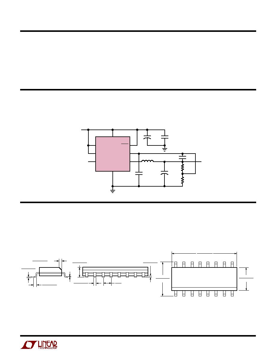
Operating Frequency and Inductor
Since the LTC1574 utilizes a constant off-time architecture,
its operating frequency is dependent on the value of V
IN
. The
frequency of operation can be expressed as:
f
t
V
V
V
V
Hz
OFF
IN
OUT
IN
D
=
-
+
( )
1
where t
OFF
= 4
µ
s and V
D
is the voltage drop across the
internal Schottky diode. Note that the operating frequency
is a function of the input and output voltage.
Although the size of the inductor does not affect the fre-
quency or inductor peak current, it does affect the ripple
current. The peak-to-peak ripple current is given by:
I
V
V
L
RIPPLE
OUT
D
=
+
( )
-
4 10
6
∑
A
P-P
When choosing a small inductor, core loss will increase due
to higher ripple current. Therefore, a low ESR output
capacitor has to be used.
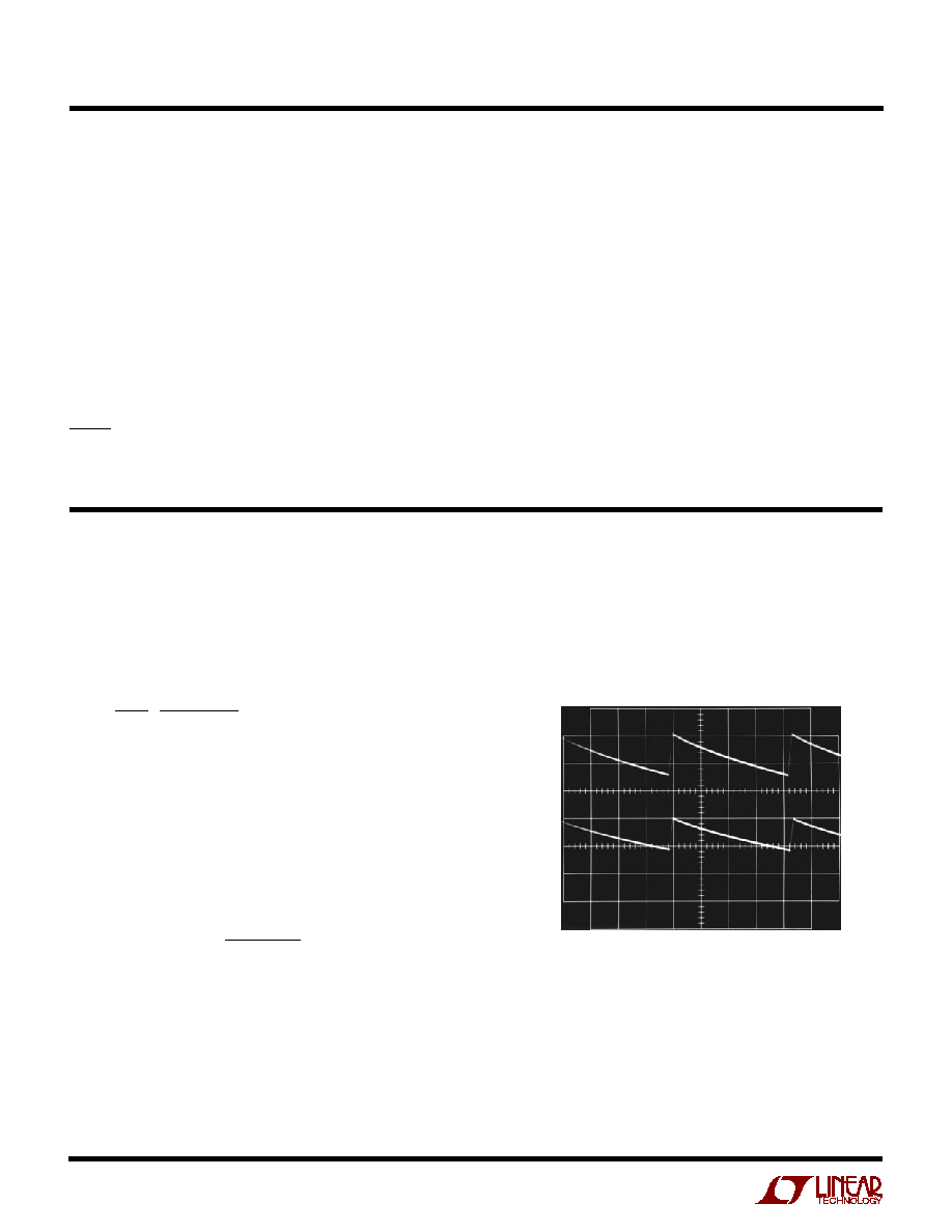
Short-Circuit Protection
The LTC1574 is protected from output short circuits by its
internal current limit. Depending on the condition of the
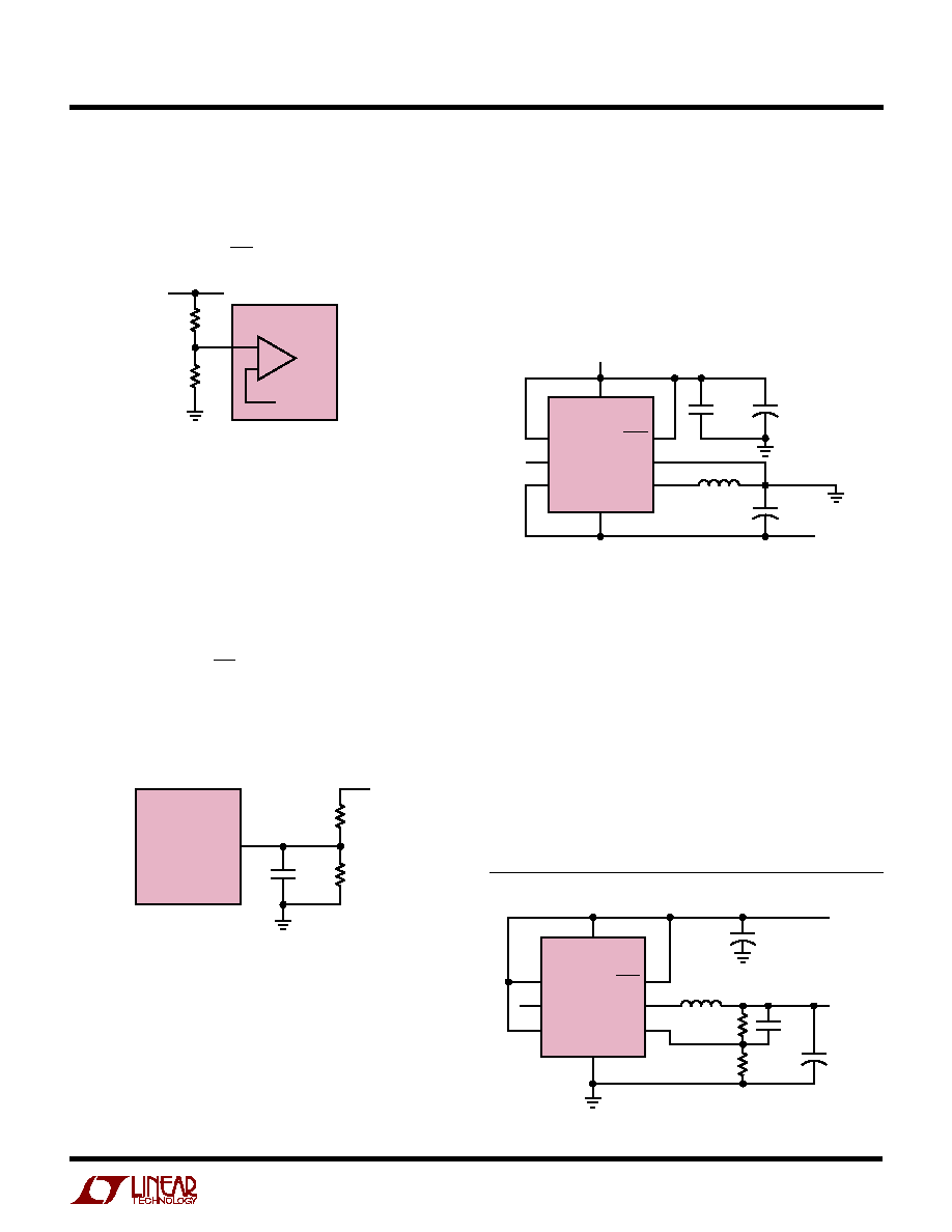
Low-Battery Detector
The low-battery indicator senses the input voltage through
an external resistive divider. This divided voltage connects
to the "≠" input of a voltage comparator (Pin 12) which is
compared with a 1.25V reference voltage. With the current
I
PGM
pin, the limit is either set to 340mA or 600mA. In
addition, the off-time of the switch is increased to allow the
inductor current to decay far enough to prevent any current
build-up (see Figure 1).
I
PGM
= V
IN
I
PGM
= 0
GND
L = 100
µ
H
V
IN
= 13.5V
100mA/DIV
20
µ
s/DIV
1574 ∑ F01
Figure 1. Inductor Current with Output Shorted
U
U
U
PI FU CTIO S
APPLICATIO S I FOR ATIO
W
U
U
U
5
LTC1574
LTC1574-3.3/LTC1574-5
going into Pin 12 being negligible, the following expres-
sion is used for setting the trip limit:
V
R
R
LBTRIP
=
+
1 25 1
4
3
.
difference between the absolute maximum voltage rating
and the output voltage. A maximum of 12V is specified in
Figure 4, giving the circuit 1.5V of headroom for V
IN
. Note
that the circuit can operate from a minimum of 4V,
making it ideal for a four NiCd cell application. For a
higher output current circuit, please refer to the Typical
Applications section.
Figure 2. Low-Battery Comparator
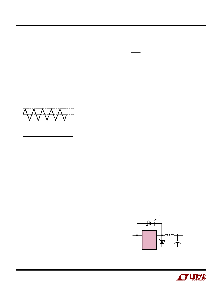
LTC1574 Adjustable Applications
The LTC1574 develops a 1.25V reference voltage between
the feedback terminal (Pin 10) and ground (see Figure 3).
By selecting resistor R1, a constant current is caused to
flow through R1 and R2 to set the overall output voltage.
The regulated output voltage is determined by:
V
R
R
OUT
=
+
1 25 1
2
1
.
For most applications, a 30k resistor is suggested for R1.
To prevent stray pickup, a 100pF capacitor is suggested
across R1 located close to the LTC1574.
Figure 3. LTC1574 Adjustable Configuration
Inverting Applications
The LTC1574 can easily be set up for a negative output
voltage. If ≠ 5V is desired, the LTC1574-5 is ideal for this
application as it requires the least components. Figure 4
shows the schematic for this application. Note that the
output voltage is now taken off the GND pins. Therefore,
the maximum input voltage is now determined by the
Figure 4. Positive-to-Negative 5V Converter
Figure 5. Low Noise 5V to 3.3V Regulator
Low Noise Regulators
In some applications it is important not to introduce any
switching noise within the audio frequency range. Due to
the nature of the LTC1574 during Burst Mode
TM
operation,
there is a possibility that the regulator will introduce audio
noise at some load currents. To circumvent this problem,
a feed-forward capacitor can be used to shift the noise
spectrum up and out of the audio band. Figure 5 shows the
low noise connection with C2 being the feed-forward
capacitor. The peak-to-peak output ripple is reduced to
30mV over the entire load range. A toroidal surface mount
Burst Mode is a trademark of Linear Technology Corporation
APPLICATIO S I FOR ATIO
W
U
U
U
LTC1574
≠
+
1.25V
REFERENCE
R4
R3
12
V
IN
1574 ∑ F02
V
FB
R2
R1
10
V
OUT
1574 ∑ F03
100pF
LTC1574
12
LTC1574-5
LB
IN
LB
OUT
I
PGM
GND
V
IN
SHDN
V
OUT
SW
11
6
5
7
10
3, 14
2, 4, 13, 15
50
µ
H**
V
OUT
≠5V
45mA
47
µ
F*
16V
◊
2
1574 ∑ F04
*
**
AVX TPSD476K016
COILTRONICS CTX50-4
INPUT VOLTAGE
4V TO 12V
0.1
µ
F
+
47
µ
F*
16V
◊
2
+
V
IN
L1**
100
µ
H
100
µ
F*
10V
1574 ∑ F05
5
2, 4, 13, 15
56k
33k
7
3, 14
10
12
11
6
V
IN
5V
V
OUT
3.3V
425mA
GND
LTC1574
LB
IN
LB
OUT
I
PGM
SHDN
SW
V
FB
* AVX TPSD107K010
** COILTRONICS CTX100-4
100
µ
F*
10V
C2
6.8nF
+
+
6
LTC1574
LTC1574-3.3/LTC1574-5
For C
OUT
, the RMS current rating should be at least:
I
I
A
RMS
PEAK
RMS
( )
=
2
300mA
Absolute Maximum Ratings and Latchup Prevention
The absolute maximum ratings specify that SW
(Pins 3, 14) can never exceed V
IN
(Pin 5) by more than
0.3V. Normally this situation should never occur. It could,
however, if the output is held up while the supply is pulled
down. A condition where this could potentially occur is
when a battery is supplying power to an LTC1574 regula-
tor and also to one or more loads in parallel with the the
regulator's V
IN
. If the battery is disconnected while the
LTC1574 regulator is supplying a light load and one of the
parallel circuits is a heavy load, the input capacitor of the
LTC1574 regulator could be pulled down faster than the
output capacitor, causing the absolute maximum ratings
to be exceeded. The result is often a latchup which can be
destructive if V
IN
is reapplied. Battery disconnect is pos-
sible as a result of mechanical stress, bad battery contacts
or use of a lithium-ion battery with a built-in internal
disconnect. The user needs to assess his/her application
to determine whether this situation could occur. If so,
additional protection is necessary.
Prevention against latchup can be accomplished by
simply connecting a Schottky diode across the SW and
V
IN
pins as shown in Figure 7. The diode will normally be
reverse biased unless V
IN
is pulled below V
OUT
at which
time the diode will clamp the (V
OUT
≠ V
IN
) potential to less
than the 0.6V required for latchup. Note that a low
leakage Schottky should be used to minimize the effect
inductor L1 is chosen for its excellent self-shielding prop-
erties. Open magnetic structures such as drum and rod
cores are to be avoided since they inject high flux levels
into their surroundings. This can become a major source
of noise in any converter circuit.
Design Example
As a design example, assume V
IN
= 9V (nominal),
V
OUT
= 5V and I
OUT
= 350mA maximum. The LTC1574-5
is used for this application with I
PGM
(Pin 6) connected to
V
IN
. The minimum value of L is determined by assuming
the LTC1574-5 is operating in continuous mode.
Figure 6. Continuous Inductor Current
With I
OUT
= 350mA and I
PEAK
= 0.6A (I
PGM
= V
IN
), I
V
= 0.1A.
The peak-to-peak ripple inductor current, I
RIPPLE
, is 0.5A
and is also equal to:
I
V
V
L
RIPPLE
OUT
D
=
+
( )
-
4 10
6
∑
A
P-P
Solving for L in the above equation and with V
D
= 0.5V,
L = 44
µ
H. The next higher standard value of L is 50
µ
H
(example: Coiltronics CTX50-4). The operating frequency,
ignoring voltage across diode V
D
is:
f
V
V
kHz
OUT
IN
-
=
2 5 10 1
111
5
. ∑
With the value of L determined, the requirements for C
IN
and C
OUT
are calculated. For C
IN
, its RMS current rating
should be at least:
I
I
V
V
V
V
A
mA
RMS
OUT
OUT
IN
OUT
IN
RMS
=
-
(
)
[
]
( )
=
1 2
174
/
INDUCTOR CURRENT
TIME
I
PEAK
I
V
AVG CURRENT = I
OUT
=
= 350mA
I
PEAK
+ I
V
2
1574 ∑ F06
APPLICATIO S I FOR ATIO
W
U
U
U
1574 F07
V
IN
V
OUT
LATCHUP
PROTECTION
SCHOTTKY
SW
LTC1574
+
Figure 7. Preventing Absolute Maximum
Ratings from Being Exceeded
7
LTC1574
LTC1574-3.3/LTC1574-5
Information furnished by Linear Technology Corporation is believed to be accurate and reliable.
However, no responsibility is assumed for its use. Linear Technology Corporation makes no represen-
tation that the interconnection of its circuits as described herein will not infringe on existing patent rights.
APPLICATIO S I FOR ATIO
W
U
U
U
on no-load supply current. Schottky diodes such as
MBR0530, BAS85 and BAT84 work well. Another more
serious effect of the protection diode leakage is that at no
load with nothing to provide a sink for this leakage
current, the output voltage can potentially float above the
maximum allowable tolerance. To prevent this from
occuring, a resistor must be connected between V
OUT
and ground with a value low enough to sink the maximum
possible leakage current.
Low Noise, High Efficiency 3.3V Regulator
TYPICAL APPLICATIO S
U
V
IN
5
100pF
2, 4, 13, 15
6
12
11
7
10
3, 14
50
µ
H
0.1
µ
F
6.8nF
22
µ
F*
25V
◊
2
1574 TA03
V
OUT
3.3V
450mA
56k
33k
V
IN
4V TO 12.5V
GND
LTC1574
I
PGM
LB
IN
LB
OUT
SHDN
V
FB
SW
* AVX TPSD226K025
** AVX TPSD107K010
COILTRONICS CTX50-4
100
µ
F**
10V
◊
2
+
+
Dimension in inches (millimeters) unless otherwise noted.
U
PACKAGE DESCRIPTIO
S Package
16-Lead Plastic Small Outline (Narrow 0.150)
(LTC DWG # 05-08-1610)
0.016 ≠ 0.050
(0.406 ≠ 1.270)
0.010 ≠ 0.020
(0.254 ≠ 0.508)
◊
45
∞
0
∞
≠ 8
∞
TYP
0.008 ≠ 0.010
(0.203 ≠ 0.254)
S16 1098
1
2
3
4
5
6
7
8
0.150 ≠ 0.157**
(3.810 ≠ 3.988)
16
15
14
13
0.386 ≠ 0.394*
(9.804 ≠ 10.008)
0.228 ≠ 0.244
(5.791 ≠ 6.197)
12
11
10
9
DIMENSION DOES NOT INCLUDE MOLD FLASH. MOLD FLASH
SHALL NOT EXCEED 0.006" (0.152mm) PER SIDE
DIMENSION DOES NOT INCLUDE INTERLEAD FLASH. INTERLEAD
FLASH SHALL NOT EXCEED 0.010" (0.254mm) PER SIDE
*
**
0.053 ≠ 0.069
(1.346 ≠ 1.752)
0.014 ≠ 0.019
(0.355 ≠ 0.483)
TYP
0.004 ≠ 0.010
(0.101 ≠ 0.254)
0.050
(1.270)
BSC
8
LTC1574
LTC1574-3.3/LTC1574-5
sn1574 1574fas LT/TP 1000 2K REV A ∑ PRINTED IN
USA
©
LINEAR TECHNOLOGY CORPORATION 1995
RELATED PARTS
Low Dropout 5V Step-Down Regulator
with Low-Battery Detection
Positive to ≠ 5V Converter
High Efficiency 3.3V Regulator
TYPICAL APPLICATIO S
U
Linear Technology Corporation
1630 McCarthy Blvd., Milpitas, CA 95035-7417
(408) 432-1900
q
FAX: (408) 434-0507
q
www.linear-tech.com
PART NUMBER
DESCRIPTION
COMMENTS
LT
Æ
1074/LT1076
Step-Down Switching Regulator
100kHz, 5A (LT1074) or 2A (LT1076) Monolithic
LTC1147
High Efficiency Step-Down DC/DC Controller
8-Pin Controller
LTC1174
High Efficiency Step-Down and Inverting DC/DC Converter 0.5A, Burst Mode Operation, SO-8 Package, V
IN
to 18V
LTC1265
1.2A High Efficiency Step-Down DC/DC Regulator
Burst Mode Operation, Monolithic
LT1375/LT1376
1.5A 500kHz Step-Down Switching Regulator
High Frequency Small Inductor
LT1611
Inverting 1.4MHz Switching Regulator in SOT-23
≠ 5V at 150mA from 5V Input, 1mV
P-P
Output Ripple, SOT-23 Package
LTC1701
1MHz Step-Down DC/DC Converter in SOT-23
V
IN
= 2.5V to 5.5V, I
Q
= 135
µ
A, V
OUT
= 5V to 1.25V
LTC1707
High Efficiency Synchronous Step-Down Regulator
V
IN
= 2.85V to 8.5V, Selectable Burst Mode Operation,
600mA Output Current, SO-8 Package
LTC1877/LTC1878
High Efficiency Synchronous Step-Down Regulator
600mA at V
IN
= 5V, 2.65V to 10V = V
IN
, I
Q
= 10
µ
A
V
IN
5
2, 4, 13, 15
6
11
12
7
10
3, 14
L1
100
µ
H
0.1
µ
F
47
µ
F**
16V
◊
2
1574 TA04
V
OUT
5V
365mA
*LOW-
BATTERY
INDICATOR
4.7k
162k
47.5k
V
IN
5.5V to 12.5V
GND
LTC1574-5
I
PGM
LB
OUT
LB
IN
SHDN
V
OUT
SW
47
µ
F**
16V
◊
2
* LOW-BATTERY INDICATOR IS
SET UP TO TRIP AT V
IN
= 5.5V
** AVX TPSD476K016
SELECTION
MANUFACTURER
PART NO.
TYPE
COILTRONICS
CTX100-4
SURFACE MOUNT
SUMIDA
CD75-101
SURFACE MOUNT
GOWANDA
GA10-103K
THROUGH HOLE
+
+
V
IN
5
2, 4, 13, 15
6
12
11
7
10
3, 14
50
µ
H
0.1
µ
F
22
µ
F*
25V
◊
2
1574 TA05
V
OUT
3.3V
425mA
V
IN
4V TO 12.5V
GND
LTC1574-3.3
I
PGM
LB
IN
LB
OUT
SHDN
V
OUT
SW
* AVX TPSD226K025
** AVX TPSD476K016
COILTRONICS CTX50-4
47
µ
F*
16V
◊
2
+
+
V
IN
5
2, 4, 13, 15
6
11
12
7
10
3, 14
L1
50
µ
H
0.1
µ
F
1574 TA06
V
OUT
≠5V
*LOW-
BATTERY
INDICATOR
4.7k
280k
43k
V
IN
4V TO 12.5V
GND
LTC1574-5
I
PGM
LB
OUT
LB
IN
SHDN
V
OUT
SW
100
µ
F***
10V
* LOW-BATTERY INDICATOR IS
SET TO TRIP AT V
IN
= 4.4V
** AVX TPSD106K035
*** AVX TPSD107K010
SELECTION
MANUFACTURER PART NO.
TYPE
COILTRONICS
CTX50-3
SURFACE MOUNT
COILCRAFT
DT3316-473 SURFACE MOUNT
SUMIDA
CD54-470
SURFACE MOUNT
GOWANDA
GA10-472K
THROUGH HOLE
10
µ
F**
35V
◊
2
V
IN
(V)
I
OUT
(mA)
4
110
6
140
8
170
10
200
12.5
235
+
+