 | –≠–ª–µ–∫—Ç—Ä–æ–Ω–Ω—ã–π –∫–æ–º–ø–æ–Ω–µ–Ω—Ç: LTC1625C | –°–∫–∞—á–∞—Ç—å:  PDF PDF  ZIP ZIP |
1
LTC1625
No R
SENSE
TM
Current Mode
Synchronous Step-Down
Switching Regulator
FEATURES
DESCRIPTIO
N
U
s
Highest Efficiency Current Mode Controller
s
No Sense Resistor Required
s
Stable High Current Operation
s
Dual N-Channel MOSFET Synchronous Drive
s
Wide V
IN
Range: 3.7V to 36V
s
Wide V
OUT
Range: 1.19V to V
IN
s
±
1% 1.19V Reference
s
Programmable Fixed Frequency with Injection Lock
s
Very Low Drop Out Operation: 99% Duty Cycle
s
Forced Continuous Mode Control Pin
s
Optional Programmable Soft Start
s
Pin Selectable Output Voltage
s
Foldback Current Limit
s
Output Overvoltage Protection
s
Logic Controlled Micropower Shutdown: I
Q
< 30
µ
A
s
Available in 16-Lead Narrow SSOP and SO Packages
The LTC
Æ
1625 is a synchronous step-down switching
regulator controller that drives external N-Channel power
MOSFETs using few external components. Current mode
control with MOSFET V
DS
sensing eliminates the need for
a sense resistor and improves efficiency. The frequency of
a nominal 150kHz internal oscillator can be synchronized
to an external clock over a 1.5:1 frequency range.
Burst Mode
TM
operation at low load currents reduces
switching losses and low dropout operation extends oper-
ating time in battery-powered systems. A forced continu-
ous mode control pin can assist secondary winding
regulation by disabling Burst Mode operation when the
main output is lightly loaded.
Fault protection is provided by foldback current limiting
and an output overvoltage comparator. An external ca-
pacitor attached to the RUN/SS pin provides soft start
capability for supply sequencing. A wide supply range
allows operation from 3.7V (3.9V for LTC1625I) to 36V at
the input and 1.19V to V
IN
at the output.
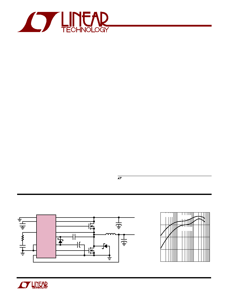
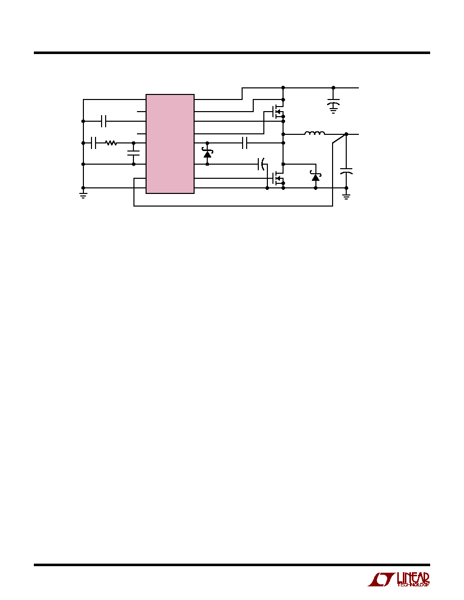
TYPICAL APPLICATIO
N
U
Figure 1. High Efficiency Step-Down Converter
+
+
V
IN
TK
SYNC
LTC1625
RUN/SS
V
OSENSE
TG
SW
C
B
0.22
µ
F
D
B
CMDSH-3
C
C
2.2nF
R
C
10k
M2
Si4410DY
D1
MBRS140T3
M1
Si4410DY
C
VCC
4.7
µ
F
1625 F01
L1
10
µ
H
C
IN
10
µ
F
30V
◊
2
BOOST
INTV
CC
BG
I
TH
V
PROG
SGND
PGND
+
C
OUT
100
µ
F
10V
◊
3
V
OUT
3.3V
4.5A
V
IN
5V TO
28V
C
SS
0.1
µ
F
LOAD CURRENT (A)
0.01
EFFICIENCY (%)
80
90
100
0.1
1
10
1625 TA01
70
60
V
IN
= 10V
V
OUT
= 5V
V
OUT
= 3.3V
Efficiency vs Load Current
APPLICATIO
N
S
U
s
Notebook and Palmtop Computers, PDAs
s
Cellular Telephones and Wireless Modems
s
Battery Chargers
s
Distributed Power
, LTC and LT are registered trademarks of Linear Technology Corporation.
No R
SENSE
and Burst Mode are trademarks of Linear Technology Corporation.
2
LTC1625
ABSOLUTE
M
AXI
M
U
M
RATINGS
W
W
W
U
(Note 1)
Input Supply Voltage (V
IN
, TK) ................. 36V to ≠ 0.3V
Boosted Supply Voltage (BOOST) ............. 42V to ≠ 0.3V
Boosted Driver Voltage (BOOST ≠ SW) ...... 7V to ≠ 0.3V
Switch Voltage (SW).....................................36V to ≠ 5V
EXTV
CC
Voltage ........................................... 7V to ≠ 0.3V
I
TH
Voltage ................................................2.7V to ≠ 0.3V
FCB, RUN/SS, SYNC Voltages .....................7V to ≠ 0.3V
V
OSENSE
, V
PROG
Voltages ........(INTV
CC
+ 0.3V) to ≠ 0.3V
Peak Driver Output Current < 10
µ
s (TG, BG) ............ 2A
INTV
CC
Output Current ........................................ 50mA
Operating Ambient Temperature Range
LTC1625C............................................... 0
∞
C to 70
∞
C
LTC1625I (Note 5) .............................. ≠ 40
∞
C to 85
∞
C
Junction Temperature (Note 2) ............................. 125
∞
C
Storage Temperature Range ................ ≠ 65
∞
C to 150
∞
C
Lead Temperature (Soldering, 10 sec)................. 300
∞
C
W
U
U
PACKAGE/ORDER I FOR ATIO
T
A
= 25
∞
C, V
IN
= 15V unless otherwise noted.
ELECTRICAL CHARACTERISTICS
SYMBOL
PARAMETER
CONDITIONS
MIN
TYP
MAX
UNITS
Main Control Loop
I
IN
V
OSENSE
Feedback Current
V
PROG
Pin Open, I
TH
= 1.19V (Note 3)
10
50
nA
V
OUT
Regulated Output Voltage
I
TH
= 1.19V (Note 3)
1.19V (Adjustable) Selected
V
PROG
Pin Open
q
1.178
1.190
1.202
V
3.3V Selected
V
PROG
= 0V
q
3.220
3.300
3.380
V
5V Selected
V
PROG
= INTV
CC
q
4.900
5.000
5.100
V
V
LINEREG
Reference Voltage Line Regulation
V
IN
= 3.6V to 20V, I
TH
= 1.19V (Note 3),
0.001
0.01
%/V
V
PROG
Pin Open
V
LOADREG
Output Voltage Load Regulation
I
TH
= 2V (Note 3)
q
≠ 0.020
≠ 0.2
%
I
TH
= 0.5V (Note 3)
q
0.035
0.2
%
V
FCB
Forced Continuous Threshold
V
FCB
Ramping Negative
q
1.16
1.19
1.22
V
I
FCB
Forced Continuous Current
V
FCB
= 1.19V
≠ 1
≠ 2
µ
A
V
OVL
Output Overvoltage Lockout
V
PROG
Pin Open
1.24
1.28
1.32
V
I
PROG
V
PROG
Input Current
3.3V V
OUT
V
PROG
= 0V
≠ 3.5
≠ 7
µ
A
5V V
OUT
V
PROG
= 5V
3.5
7
µ
A
I
Q
Input DC Supply Current
EXTV
CC
= 5V (Note 4)
Normal Mode
500
µ
A
Shutdown
V
RUN/SS
= 0V, 3.7V < V
IN
< 15V
15
30
µ
A
V
RUN/SS
RUN/SS Pin Threshold
q
0.8
1.4
2
V
I
RUN/SS
Soft Start Current Source
V
RUN/SS
= 0V
1.2
2.5
4
µ
A
V
SENSE(MAX)
Maximum Current Sense Threshold
V
OSENSE
= 1V, V
PROG
Pin Open
120
150
170
mV
TG Transition Time
TG t
R
Rise Time
C
LOAD
= 3300pF
50
150
ns
TG t
F
Fall Time
C
LOAD
= 3300pF
50
150
ns
ORDER PART
NUMBER
LTC1625CGN
LTC1625CS
LTC1625IGN
LTC1625IS
Consult factory for Military grade parts.
TOP VIEW
S PACKAGE
16-LEAD PLASTIC SO
GN PACKAGE
16-LEAD PLASTIC SSOP
1
2
3
4
5
6
7
8
16
15
14
13
12
11
10
9
EXTV
CC
SYNC
RUN/SS
FCB
I
TH
SGND
V
OSENSE
V
PROG
V
IN
TK
SW
TG
BOOST
INTV
CC
BG
PGND
T
JMAX
= 125
∞
C,
JA
= 130
∞
C/W (GN)
T
JMAX
= 125
∞
C,
JA
= 110
∞
C/W (S)
3
LTC1625
T
A
= 25
∞
C, V
IN
= 15V unless otherwise noted.
ELECTRICAL CHARACTERISTICS
SYMBOL
PARAMETER
CONDITIONS
MIN
TYP
MAX
UNITS
BG Transition Time
BG t
R
Rise Time
C
LOAD
= 3300pF
50
150
ns
BG t
F
Fall Time
C
LOAD
= 3300pF
50
150
ns
Internal V
CC
Regulator
V
INTVCC
Internal V
CC
Voltage
6V < V
IN
< 30V, V
EXTVCC
= 4V
q
5.0
5.2
5.4
V
V
LDOINT
INTV
CC
Load Regulation
I
CC
= 20mA, V
EXTVCC
= 4V
≠ 1
≠ 2
%
V
LDOEXT
EXTV
CC
Voltage Drop
I
CC
= 20mA, V
EXTVCC
= 5V
180
300
mV
V
EXTVCC
EXTV
CC
Switchover Voltage
I
CC
= 20mA, V
EXTVCC
Ramping Positive
q
4.5
4.7
V
Oscillator
f
OSC
Oscillator Freqency
135
150
165
kHz
f
H
/f
OSC
Maximum Synchronized Frequency Ratio
1.5
V
SYNC
SYNC Pin Threshold (Figure 4)
Ramping Positive
0.9
1.2
V
R
SYNC
SYNC Pin Input Resistance
50
k
The
q
denotes specifications which apply over the full operating
temperature range.
Note 1: Absolute Maximum Ratings are those values beyond which the life
of a device may be impaired.
Note 2: T
J
is calculated from the ambient temperature T
A
and power
dissipation P
D
according to the following formula:
LTC1625CGN/LTC1625IGN: T
J
= T
A
+ (P
D
∑ 130
∞
C/W)
LTC1625CS/LTC1625IS: T
J
= T
A
+ (P
D
∑ 110
∞
C/W)
Note 3: The LTC1625 is tested in a feedback loop that adjusts V
OSENSE
to
achieve a specified error amplifier output voltage (I
TH
).
Note 4: Typical in application circuit with EXTV
CC
tied to V
OUT
= 5V,
I
OUT
= 0A and FCB = INTV
CC
. Dynamic supply current is higher due
to the gate charge being delivered at the switching frequency. See
Applications Information.
Note 5: Minimum input supply voltage is 3.9V at ≠ 40
∞
C for industrial
grade parts.
4
LTC1625
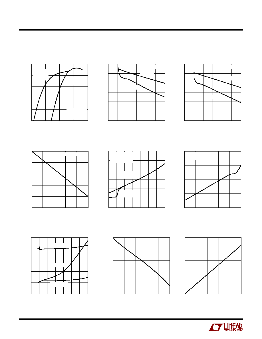
TYPICAL PERFOR A CE CHARACTERISTICS
U
W
INPUT VOLTAGE (V)
0
70
EFFICIENCY (%)
75
80
85
90
100
5
10
15
20
1625 G02
25
30
95
I
LOAD
= 2A
I
LOAD
= 200mA
FIGURE 1 CIRCUIT
Efficiency vs Input Voltage,
V
OUT
= 3.3V
V
IN
≠ V
OUT
Dropout Voltage
vs Load Current
LOAD CURRENT (A)
0
V
IN
≠ V
OUT
(mV)
200
300
4
1625 G06
100
0
1
2
3
5
400
FIGURE 1 CIRCUIT
V
OUT
= 5V ≠ 5% DROP
Efficiency vs Load Current
LOAD CURRENT (A)
0.001
EFFICIENCY (%)
70
80
10
1625 G01
60
50
0.01
0.1
1
100
90
BURST
MODE
OPERATION
CONTINUOUS
MODE
V
IN
= 10V
V
OUT
= 5V
EXTV
CC
= V
OUT
Load Regulation
LOAD CURRENT (A)
0
V
OUT
(%)
≠ 0.10
≠ 0.05
0
4
1625 G04
≠ 0.15
≠ 0.20
≠ 0.25
1
2
3
5
FIGURE 1 CIRCUIT
Input and Shutdown Current
vs Input Voltage
INPUT VOLTAGE (V)
0
5
0
INPUT CURRENT (
µ
A)
SHUTDOWN CURRENT (
µ
A)
400
1000
10
20
25
1625 G07
200
800
600
0
20
50
10
40
30
15
30
35
EXTV
CC
OPEN
EXTV
CC
= 5V
SHUTDOWN
Efficiency vs Input Voltage,
V
OUT
= 5V
INPUT VOLTAGE (V)
0
70
EFFICIENCY (%)
75
80
85
90
100
5
10
15
20
1625 G02
25
30
95
I
LOAD
= 2A
I
LOAD
= 200mA
FIGURE 1 CIRCUIT
I
TH
Pin Voltage vs Load Current
LOAD CURRENT (A)
0
V
ITH
(V)
2.0
2.5
3.0
3
5
1625 G05
1.5
1.0
1
2
4
6
7
0.5
0
FIGURE 1 CIRCUIT
V
IN
= 20V
V
OUT
= 5V
CONTINUOUS
MODE
Burst Mode
OPERATION
INTV
CC
LOAD CURRENT (mA)
0
EXTV
CC
≠ INTV
CC
(mV)
300
400
500
40
1625 G09
200
100
0
10
20
30
50
EXTV
CC
Switch Drop
vs INTV
CC
Load Current
INTV
CC
Load Regulation
INTV
CC
LOAD CURRENT (mA)
0
INTV
CC
(%)
≠1.0
≠ 0.5
0
40
1625 G08
≠1.5
≠ 2.0
≠ 2.5
10
20
30
50
5
LTC1625
TYPICAL PERFOR A CE CHARACTERISTICS
U
W
Oscillator Frequency
vs Temperature
FCB Pin Current vs Temperature
Maximum Current Sense Voltage
vs Temperature
Maximum Current Sense Voltage
vs Duty Cycle
DUTY CYCLE
0
MAXIMUM CURRENT SENSE VOLTAGE (mV)
100
150
0.8
1625 G10
50
0
0.2
0.4
0.5
1.0
200
TEMPERATURE (
∞
C)
≠ 40
140
MAXIMUM CURRENT SENSE VOLTAGE (mV)
145
150
155
160
≠15
10
35
60
1625 G11
85
110
135
TEMPERATURE (
∞
C)
≠ 40
FREQUENCY (kHz)
200
250
300
35
85
1625 G12
150
100
≠15
10
60
110
135
50
0
SYNC = 1.5V
SYNC = 0V
TEMPERATURE (
∞
C)
≠ 40
FCB CURRENT (
µ
A) ≠0.50
≠ 0.25
0
35
85
1625 G13
≠ 0.75
≠1.00
≠15
10
60
110
135
≠1.25
≠1.50
RUN/SS Pin Current
vs Temperature
TEMPERATURE (
∞
C)
≠40
≠15
≠ 5
RUN/SS CURRENT (
µ
A)
≠ 3
0
10
60
85
1625 G14
≠ 4
≠ 1
≠ 2
35
110
135
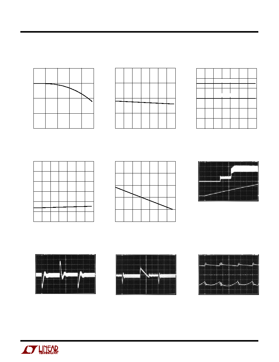
Soft Start:
Load Current vs Time
INDUCTOR
CURRENT
2A/DIV
RUN/SS
2V/DIV
20ms/DIV
V
IN
= 20V
V
OUT
= 5V
R
LOAD
= 1
FIGURE 1 CIRCUIT
V
IN
= 20V
V
OUT
= 5V
I
LOAD
= 1A TO 4A
FIGURE 1 CIRCUIT
V
OUT
50mV/DIV
200
µ
s/DIV
50
µ
s/DIV
V
IN
= 20V
V
OUT
= 5V
I
LOAD
= 50mA
FIGURE 1 CIRCUIT
Burst Mode Operation
V
OUT
50mV/DIV
I
TH
100mV/DIV
Transient Response
(Burst Mode Operation)
V
OUT
50mV/DIV
500
µ
s/DIV
V
IN
= 20V
V
OUT
= 5V
I
LOAD
= 50mA TO 1A
FIGURE 1 CIRCUIT
Transient Response
1625 F07
1625 F09
1625 F06
1625 F08

6
LTC1625
PI
N
FU
N
CTIO
N
S
U
U
U
Leaving V
PROG
open allows the output voltage to be set by
an external resistive divider between the output and
V
OSENSE
.
PGND (Pin 9): Driver Power Ground. Connects to the
source of the bottom N-channel MOSFET, the (≠) terminal
of C
VCC
and the (≠) terminal of C
IN
.
BG (Pin 10): Bottom Gate Drive. Drives the gate of the
bottom N-channel MOSFET between ground and INTV
CC
.
INTV
CC
(Pin 11): Internal 5.2V Regulator Output. The
driver and control circuits are powered from this voltage.
Decouple this pin to power ground with a minimum of
4.7
µ
F tantalum capacitance.
BOOST (Pin 12): Topside Floating Driver Supply. The (+)
terminal of the bootstrap capacitor connects here. This pin
swings from a diode drop below INTV
CC
to V
IN
+ INTV
CC
.
TG (Pin 13): Top Gate Drive. Drives the top N-channel
MOSFET with a voltage swing equal to INTV
CC
minus a
diode drop, superimposed on the switch node voltage.
SW (Pin 14): Switch Node. The (≠) terminal of the boot-
strap capacitor connects here. This pin swings from a
diode drop below ground up to V
IN
.
TK (Pin 15): Top MOSFET Kelvin Sense. MOSFET V
DS
sensing requires this pin to be routed to the drain of the top
MOSFET separately from V
IN
.
V
IN
(Pin 16): Main Supply Input. Decouple this pin to
ground with an RC filter (4.7
, 0.1
µ
F) for applications
above 3A.
EXTV
CC
(Pin 1): INTV
CC
Switch Input. When the EXTV
CC
voltage is above 4.7V, the switch closes and supplies
INTV
CC
power from EXTV
CC
. Do not exceed 7V at this pin.
SYNC (Pin 2): Synchronization Input for Internal Oscilla-
tor. The oscillator will nominally run at 150kHz when open,
225kHz when tied above 1.2V, and will lock over a 1.5:1
clock frequency range.
RUN/SS (Pin 3): Run Control and Soft Start Input. A
capacitor to ground at this pin sets the ramp time to full
current output (approximately 1s/
µ
F). Forcing this pin
below 1.4V shuts down the device.
FCB (Pin 4): Forced Continuous Input. Tie this pin to
ground to force synchronous operation at low load, to a
resistive divider from the secondary output when using
a secondary winding, or to INTV
CC
to enable Burst Mode
operation at low load.
I
TH
(Pin 5): Error Amplifier Compensation Point. The
current comparator threshold increases with this control
voltage. Nominal voltage range for this pin is 0V to 2.4V.
SGND (Pin 6): Signal Ground. Connect to the (≠) terminal
of C
OUT
.
V
OSENSE
(Pin 7): Output Voltage Sense. Feedback input
from the remotely sensed output voltage or from an
external resistive divider across the output.
V
PROG
(Pin 8): Output Voltage Programming. When
V
OSENSE
is connected to the output, V
PROG
< 0.8V selects
a 3.3V output and V
PROG
> 3.5V selects a 5V output.
7
LTC1625
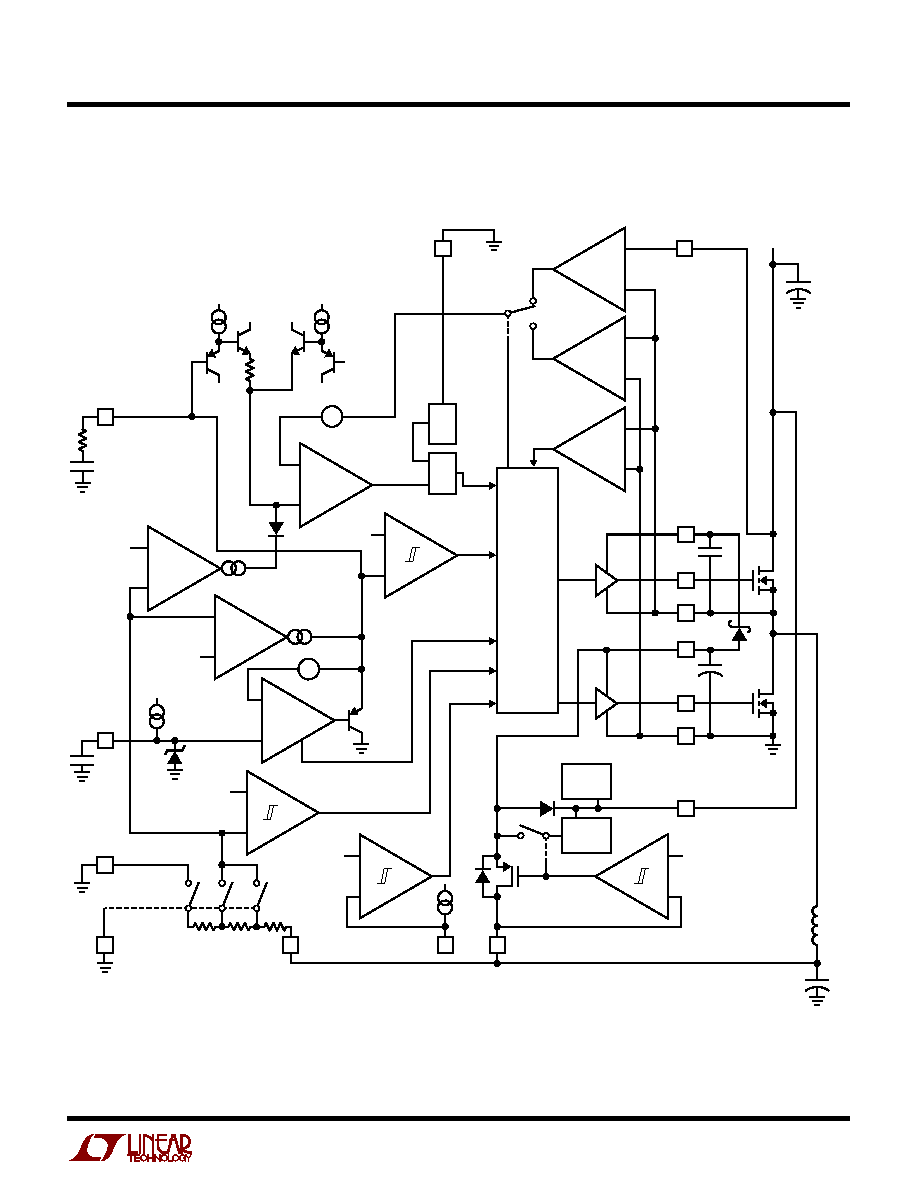
FU
N
CTIO
N
AL DIAGRA
U
U
W
+
INTV
CC
C
VCC
+
C
IN
M2
V
IN
16
EXTV
CC
FCB
1
4
V
PROG
8
SGND
6
RUN/SS
3
BG
10
PGND
4.7V
1.19V
C
SS
1
µ
A
L1
1625 BD
9
BOOST
V
IN
C
B
M1
D
B
12
TK
REV
15
SYNC
2
TG
13
SW
14
SWITCH
LOGIC/
DROPOUT
COUNTER
≠
+
≠
+
≠
+
≠
+
TA
◊
11
BA
◊
11
I
2
1.19V
REF
FCNT
OVERVOLTAGE
SHUTDOWN
TOP
0.6V
5.2V
LDO REG
1.28V
1.19V
V
FB
≠
+
≠
+
≠
+
≠
+
+
C
OUT
3
µ
A
6V
0.6V
g
m
= 1m
≠
+
CL
V
OSENSE
7
+ ≠
0.6V
0.95V
I
TH
5
C
C1
R
C
SLEEP
0.5V
I
THB
≠
+
≠
+
I
1
S
OSC
Q
R
B
+ ≠
F
OV
EA
11

8
LTC1625
OPERATIO
U
Main Control Loop
The LTC1625 is a constant frequency, current mode
controller for DC/DC step-down converters. In normal
operation, the top MOSFET is turned on when the RS latch
is set by the on-chip oscillator and is turned off when the
current comparator I
1
resets the latch. While the top
MOSFET is turned off, the bottom MOSFET is turned on
until either the inductor current reverses, as determined
by the current reversal comparator I
2
, or the next cycle
begins. Inductor current is measured by sensing the V
DS
potential across the conducting MOSFET. The output of
the appropriate sense amplifier (TA or BA) is selected by
the switch logic and applied to the current comparator.
The voltage on the I
TH
pin sets the comparator threshold
corresponding to peak inductor current. The error ampli-
fier EA adjusts this voltage by comparing the feedback
signal V
FB
from the output voltage with the internal 1.19V
reference. The V
PROG
pin selects whether the feedback
voltage is taken directly from the V
OSENSE
pin or is derived
from an on-chip resistive divider. When the load current
increases, it causes a drop in the feedback voltage relative
to the reference. The I
TH
voltage then rises until the
average inductor current again matches the load current.
The internal oscillator can be synchronized to an external
clock applied to the SYNC pin and can lock to a frequency
between 100% and 150% of its nominal 150kHz rate.
When the SYNC pin is left open, it is pulled low internally
and the oscillator runs at its normal rate. If this pin is taken
above 1.2V, the oscillator will run at its maximum 225kHz
rate.
Pulling the RUN/SS pin low forces the controller into its
shutdown state and turns off both MOSFETs. Releasing
the RUN/SS pin allows an internal 3
µ
A current source to
charge up an external soft start capacitor C
SS
. When this
voltage reaches 1.4V, the controller begins switching, but
with the I
TH
voltage clamped at approximately 0.8V. As
C
SS
continues to charge, the clamp is raised until full range
operation is restored.
The top MOSFET driver is powered from a floating boot-
strap capacitor C
B
. This capacitor is normally recharged
from INTV
CC
through a diode D
B
when the top MOSFET is
turned off. As V
IN
decreases towards V
OUT
, the converter
will attempt to turn on the top MOSFET continuously
(`'dropout''). A dropout counter detects this condition and
forces the top MOSFET to turn off for about 500ns every
tenth cycle to recharge the bootstrap capacitor.
An overvoltage comparator OV guards against transient
overshoots and other conditions that may overvoltage the
output. In this case, the top MOSFET is turned off and the
bottom MOSFET is turned on until the overvoltage condi-
tion is cleared.
Foldback current limiting for an output shorted to ground
is provided by a transconductance amplifer CL. As V
FB
drops below 0.6V, the buffered I
TH
input to the current
comparator is gradually pulled down to a 0.95V clamp.
This reduces peak inductor current to about one fifth of its
maximum value.
Low Current Operation
The LTC1625 is capable of Burst Mode operation at low
load currents. If the error amplifier drives the I
TH
voltage
below 0.95V, the buffered I
TH
input to the current com-
parator will remain clamped at 0.95V. The inductor current
peak is then held at approximately 30mV/R
DS(ON)(TOP)
. If
I
TH
then drops below 0.5V, the Burst Mode comparator B
will turn off both MOSFETs. The load current will be
supplied solely by the output capacitor until I
TH
rises
above the 50mV hysteresis of the comparator and switch-
ing is resumed. Burst Mode operation is disabled by
comparator F when the FCB pin is brought below 1.19V.
This forces continuous operation and can assist second-
ary winding regulation.
INTV
CC
/EXTV
CC
Power
Power for the top and bottom MOSFET drivers and most
of the internal circuitry of the LTC1625 is derived from the
INTV
CC
pin. When the EXTV
CC
pin is left open, an internal
5.2V low dropout regulator supplies the INTV
CC
power
from V
IN
. If EXTV
CC
is raised above 4.7V, the internal
regulator is turned off and an internal switch connects
EXTV
CC
to INTV
CC
. This allows a high efficiency source,
such as the primary or a secondary output of the converter
itself, to provide the INTV
CC
power.
9
LTC1625
APPLICATIO
N
S I
N
FOR
M
ATIO
N
W
U
U
U
The basic LTC1625 application circuit is shown in Figure 1.
External component selection is primarily determined by
the maximum load current and begins with the selection of
the sense resistance and power MOSFETs. Because the
LTC1625 uses MOSFET V
DS
sensing, the sense resistance
is the R
DS(ON)
of the MOSFETs. The operating frequency
and the inductor are chosen based largely on the desired
amount of ripple current. Finally, C
IN
is selected for its
ability to handle the large RMS current into the converter
and C
OUT
is chosen with low enough ESR to meet the
output voltage ripple specification.
Power MOSFET Selection
The LTC1625 requires two external N-channel power
MOSFETs, one for the top (main) switch and one for the
bottom (synchronous) switch. Important parameters for
the power MOSFETs are the breakdown voltage V
(BR)DSS
,
threshold voltage V
GS(TH)
, on-resistance R
DS(ON)
, reverse
transfer capacitance C
RSS
and maximum current I
D(MAX)
.
The gate drive voltage is set by the 5.2V INTV
CC
supply.
Consequently, logic level threshold MOSFETs must be
used in LTC1625 applications. If low input voltage opera-
tion is expected (V
IN
< 5V), then sub-logic level threshold
MOSFETs should be used. Pay close attention to the
V
(BR)DSS
specification for the MOSFETs as well; many of
the logic level MOSFETs are limited to 30V or less.
The MOSFET on-resistance is chosen based on the
required load current. The maximum average output cur-
rent I
O(MAX)
is equal to the peak inductor current less half
the peak-to-peak ripple current
I
L
. The peak inductor
current is inherently limited in a current mode controller
by the current threshold I
TH
range. The corresponding
maximum V
DS
sense voltage is about 150mV under nor-
mal conditions. The LTC1625 will not allow peak inductor
current to exceed 150mV/R
DS(ON)(TOP)
. The following
equation is a good guide for determining the required
R
DS(ON)(MAX)
at 25
∞
C (manufacturer's specification), al-
lowing some margin for ripple current, current limit and
variations in the LTC1625 and external component values:
R
mV
I
DS ON MAX
O MAX
T
(
)(
)
(
)
(
)( )
120
The
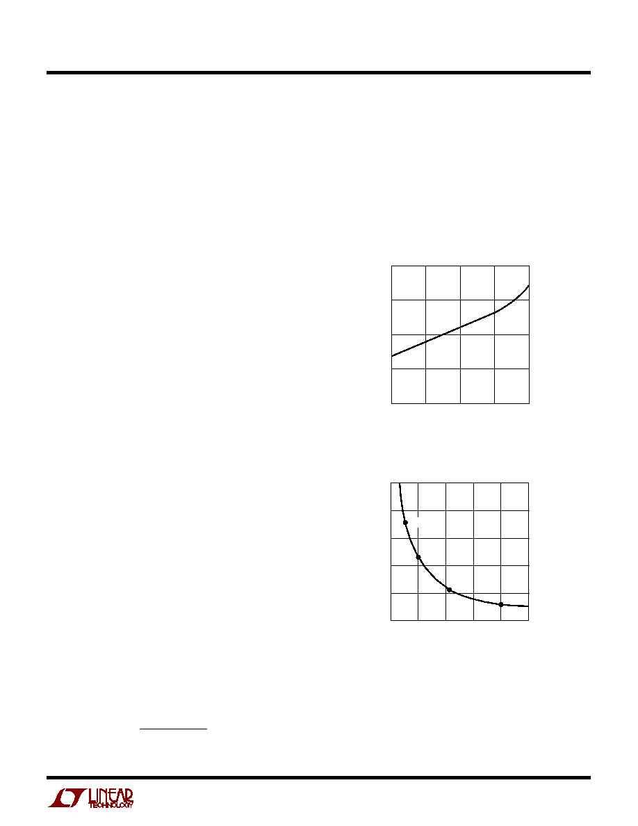
T
is a normalized term accounting for the significant
variation in R
DS(ON)
with temperature, typically about
0.4%/
∞
C as shown in Figure 2. Junction to case tempera-
ture T
JC
is around 10
∞
C in most applications. For a
maximum ambient temperature of 70
∞
C, using
80
∞
C
1.3
in the above equation is a reasonable choice. This equation
is plotted in Figure 3 to illustrate the dependence of
maximum output current on R
DS(ON)
. Some popular
MOSFETs from Siliconix are shown as data points.
JUNCTION TEMPERATURE (
∞
C)
≠ 50
T
NORMALIZED ON RESISTANCE
1.0
1.5
150
1625 F02
0.5
0
0
50
100
2.0
Figure 2. R
DS(ON)
vs Temperature
R
DS(ON)
(
)
0
MAXIMUM OUTPUT CURRENT (A)
6
8
10
0.08
1625 F03
4
2
0
0.02
0.04
0.06
0.10
Si4420
Si4410
Si4412
Si9936
Figure 3. Maximum Output Current vs R
DS(ON)
at V
GS
= 4.5V
The power dissipated by the top and bottom MOSFETs
strongly depends upon their respective duty cycles and
the load current. When the LTC1625 is operating in con-
tinuous mode, the duty cycles for the MOSFETs are:
10
LTC1625
APPLICATIO
N
S I
N
FOR
M
ATIO
N
W
U
U
U
Top Duty Cycle
V
V
Bottom Duty Cycle
V
V
V
OUT
IN
IN
OUT
IN
=
=
≠
The MOSFET power dissipations at maximum output
current are:
P
V
V
I
R
k V
I
C
f
P
V
V
V
I
R
TOP
OUT
IN
O MAX
T TOP
DS ON
IN
O MAX
RSS
BOT
IN
OUT
IN
O MAX
T BOT
DS ON
=
+
=
(
)(
)(
)
( )(
)(
)(
)( )
≠
(
)(
)(
)
(
)
(
)
(
)
(
)
(
)
(
)
(
)
2
2
2
Both MOSFETs have I
2
R losses and the P
TOP
equation
includes an additional term for transition losses, which are
largest at high input voltages. The constant k = 1.7 can be
used to estimate the amount of transition loss. The bottom
MOSFET losses are greatest at high input voltage or during
a short circuit when the duty cycle is nearly 100%.
Operating Frequency and Synchronization
The choice of operating frequency and inductor value is a
trade-off between efficiency and component size. Low
frequency operation improves efficiency by reducing
MOSFET switching losses, both gate charge loss and
transition loss. However, lower frequency operation
requires more inductance for a given amount of ripple
current.
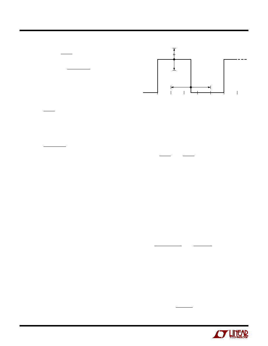
The internal oscillator runs at a nominal 150kHz frequency
when the SYNC pin is left open or connected to ground.
Pulling the SYNC pin above 1.2V will increase the fre-
quency by 50%. The oscillator will injection lock to a clock
signal applied to the SYNC pin with a frequency between
165kHz and 200kHz. The clock high level must exceed
1.2V for at least 1
µ
s and no longer than 4
µ
s as shown in
Figure 4. The top MOSFET turn-on will synchronize with
the rising edge of the clock.
0
±
1
µ
s
4
µ
s
1625 F04
7V
1.2V
Figure 4. SYNC Clock Waveform
Inductor Value Selection
Given the desired input and output voltages, the inductor
value and operating frequency directly determine the
ripple current:
I
V
f L
V
V
L
OUT
OUT
IN
=
( )( )
≠
1
Lower ripple current reduces core losses in the inductor,
ESR losses in the output capacitors and output voltage
ripple. Thus, highest efficiency operation is obtained at
low frequency with small ripple current. To achieve this,
however, requires a large inductor.
A reasonable starting point is to choose a ripple current
that is about 40% of I
O(MAX)
. Note that the largest ripple
current occurs at the highest V
IN
. To guarantee that ripple
current does not exceed a specified maximum, the induc-
tor should be chosen according to:
L
V
f
I
V
V
OUT
L MAX
OUT
IN MAX
( )(
)
≠
(
)
(
)
1
Burst Mode Operation Considerations
The choice of R
DS(ON)
and inductor value also determines
the load current at which the LTC1625 enters Burst Mode
operation. When bursting, the controller clamps the peak
inductor current to approximately:
I
mV
R
BURST PEAK
DS ON
(
)
(
)
=
30

11
LTC1625
APPLICATIO
N
S I
N
FOR
M
ATIO
N
W
U
U
U
The corresponding average current depends on the amount
of ripple current. Lower inductor values (higher
I
L
) will
reduce the load current at which Burst Mode operation
begins.
The output voltage ripple can increase during Burst Mode
operation if
I
L
is substantially less than I
BURST
. This will
primarily occur when the duty cycle is very close to unity
(V
IN
is close to V
OUT
) or if very large value inductors are
chosen. This is generally only a concern in applications
with V
OUT
5V. At high duty cycles, a skipped cycle
causes the inductor current to quickly descend to zero.
However, it takes multiple cycles to ramp the current back
up to I
BURST(PEAK)
. During this interval, the output capaci-
tor must supply the load current and enough charge may
be lost to cause significant droop in the output voltage. It
is a good idea to keep
I
L
comparable to I
BURST(PEAK)
.
Otherwise, one might need to increase the output capaci-
tance in order to reduce the voltage ripple or else disable
Burst Mode operation by forcing continuous operation
with the FCB pin.
Fault Conditions: Current Limit and Output Shorts
The LTC1625 current comparator can accommodate a
maximum sense voltage of 150mV. This voltage and the
sense resistance determine the maximum allowed peak
inductor current. The corresponding output current limit
is:
I
mV
R
I
LIMIT
DS ON
T
L
=
(
)( )
150
1
2
(
)
≠
The current limit value should be checked to ensure that
I
LIMIT(MIN)
> I
O(MAX)
. The minimum value of current limit
generally occurs with the largest V
IN
at the highest ambi-
ent temperature, conditions which cause the highest power
dissipation in the top MOSFET. Note that it is important to
check for self-consistency between the assumed junction
temperature of the top MOSFET and the resulting value of
I
LIMIT
which heats the junction.
Caution should be used when setting the current limit
based upon R
DS(ON)
of the MOSFETs. The maximum
current limit is determined by the minimum MOSFET on-
resistance. Data sheets typically specify nominal and
maximum values for R
DS(ON)
, but not a minimum. A
reasonable, but perhaps overly conservative, assumption
is that the minimum R
DS(ON)
lies the same amount below
the typical value as the maximum R
DS(ON)
lies above it.
Consult the MOSFET manufacturer for further guidelines.
The LTC1625 includes current foldback to help further
limit load current when the output is shorted to ground. If
the output falls by more than half, then the maximum
sense voltage is progressively lowered from 150mV to
30mV. Under short-circuit conditions with very low duty
cycle, the LTC1625 will begin skipping cycles in order to
limit the short-circuit current. In this situation the bottom
MOSFET R
DS(ON)
will control the inductor current trough
rather than the top MOSFET controlling the inductor
current peak. The short-circuit ripple current is deter-
mined by the minimum on-time t
ON(MIN)
of the LTC1625
(approximately 0.5
µ
s), the input voltage, and inductor
value:
I
L(SC)
= t
ON(MIN)
V
IN
/L.
The resulting short-circuit current is:
I
mV
R
I
SC
DS ON BOT
T
L SC
=
(
)( )
+
30
1
2
(
)(
)
(
)
Normally, the top and bottom MOSFETs will be of the same
type. A bottom MOSFET with lower R
DS(ON)
than the top
may be chosen if the resulting increase in short-circuit
current is tolerable. However, the bottom MOSFET should
never be chosen to have a higher nominal R
DS(ON)
than the
top MOSFET.
Inductor Core Selection
Once the value for L is known, the type of inductor must be
selected. High efficiency converters generally cannot
afford the core loss found in low cost powdered iron cores,
forcing the use of more expensive ferrite, molypermalloy
or Kool M
µ
Æ
cores. Actual core loss is independent of core
size for a fixed inductor value, but it is very dependent on
the inductance selected. As inductance increases, core
losses go down. Unfortunately, increased inductance
requires more turns of wire and therefore copper losses
will increase.
Kool M
µ
is a registered trademark of Magnetics, Inc.

12
LTC1625
APPLICATIO
N
S I
N
FOR
M
ATIO
N
W
U
U
U
Ferrite designs have very low core loss and are preferred
at high switching frequencies, so design goals can con-
centrate on copper loss and preventing saturation. Ferrite
core material saturates "hard," which means that induc-
tance collapses rapidly when the peak design current is
exceeded. This results in an abrupt increase in inductor
ripple current and consequent output voltage ripple. Do
not allow the core to saturate!
Molypermalloy (from Magnetics, Inc.) is a very good, low
loss core material for toroids, but it is more expensive than
ferrite. A reasonable compromise from the same manu-
facturer is Kool M
µ
. Toroids are very space efficient,
especially when you can use several layers of wire.
Because they generally lack a bobbin, mounting is more
difficult. However, designs for surface mount are available
which do not increase the height significantly.
Schottky Diode Selection
The Schottky diode D1 shown in Figure 1 conducts during
the dead time between the conduction of the power
MOSFETs. This prevents the body diode of the bottom
MOSFET from turning on and storing charge during the
dead time, which could cost as much as 1% in efficiency.
A 1A Schottky diode is generally a good size for 3A to 5A
regulators. The diode may be omitted if the efficiency loss
can be tolerated.
C
IN
and C
OUT
Selection
In continuous mode, the drain current of the top MOSFET
is approximately a square wave of duty cycle V
OUT
/ V
IN
. To
prevent large input voltage transients, a low ESR input
capacitor sized for the maximum RMS current must be
used. The maximum RMS current is given by:
I
I
V
V
V
V
RMS
O MAX
OUT
IN
IN
OUT
-
(
)
/
1
1 2
This formula has a maximum at V
IN
= 2V
OUT
, where I
RMS
= I
O(MAX)
/2. This simple worst-case condition is com-
monly used for design because even significant deviations
do not offer much relief. Note that ripple current ratings
from capacitor manufacturers are often based on only
2000 hours of life. This makes it advisable to further derate
the capacitor or to choose a capacitor rated at a higher
temperature than required. Several capacitors may also be
placed in parallel to meet size or height requirements in the
design.
The selection of C
OUT
is primarily determined by the ESR
required to minimize voltage ripple. The output ripple
V
OUT
is approximately bounded by:
V
I ESR
f C
OUT
L
OUT
+
1
8
( )( )(
)
Since
I
L
increases with input voltage, the output ripple is
highest at maximum input voltage. Typically, once the ESR
requirement is satisfied the capacitance is adequate for
filtering and has the required RMS current rating.
Manufacturers such as Nichicon, United Chemicon and
Sanyo should be considered for high performance through-
hole capacitors. The OS-CON semiconductor dielectric
capacitor available from Sanyo has the lowest product of
ESR and size of any aluminum electrolytic at a somewhat
higher price.
In surface mount applications, multiple capacitors may
have to be placed in parallel to meet the ESR requirement.
Aluminum electrolytic and dry tantalum capacitors are
both available in surface mount packages. In the case of
tantalum, it is critical that the capacitors have been surge
tested for use in switching power supplies. An excellent
choice is the AVX TPS series of surface mount tantalum,
available in case heights ranging from 2mm to 4mm. Other
capacitor types include Sanyo OS-CON, Nichicon PL se-
ries, and Sprague 593D and 595D series. Consult the
manufacturer for other specific recommendations.
INTV
CC
Regulator
An internal P-channel low dropout regulator produces the
5.2V supply which powers the drivers and internal cir-
cuitry within the LTC1625. The INTV
CC
pin can supply up
to 50mA and must be bypassed to ground with a minimum
of 4.7
µ
F tantalum or low ESR electrolytic capacitance.
Good bypassing is necessary to supply the high transient
currents required by the MOSFET gate drivers.
13
LTC1625
APPLICATIO
N
S I
N
FOR
M
ATIO
N
W
U
U
U
High input voltage applications in which large MOSFETs
are being driven at high frequencies may cause the LTC1625
to exceed its maximum junction temperature rating. Most
of the supply current drives the MOSFET gates unless an
external EXTV
CC
source is used. The junction temperature
can be estimated from the equations given in Note 2 of the
Electrical Characteristics. For example, the LTC1625CGN
is limited to less than 14mA from a 30V supply:
T
J
= 70
∞
C + (14mA)(30V)(130
∞
C/W) = 125
∞
C
To prevent the maximum junction temperature from being
exceeded, the input supply current must be checked when
operating in continuous mode at high V
IN
.
EXTV
CC
Connection
The LTC1625 contains an internal P-channel MOSFET
switch connected between the EXTV
CC
and INTV
CC
pins.
Whenever the EXTV
CC
pin is above 4.7V the internal 5.2V
regulator shuts off, the switch closes and INTV
CC
power is
supplied via EXTV
CC
until EXTV
CC
drops below 4.5V. This
allows the MOSFET gate drive and control power to be
derived from the output or other external source during
normal operation. When the output is out of regulation
(start-up, short circuit) power is supplied from the internal
regulator. Do not apply greater than 7V to the EXTV
CC
pin
and ensure that EXTV
CC
V
IN
.
Significant efficiency gains can be realized by powering
INTV
CC
from the output, since the V
IN
current supplying
the driver and control currents will be scaled by a factor of
Duty Cycle/Efficiency. For 5V regulators this simply means
connecting the EXTV
CC
pin directly to V
OUT
. However, for
3.3V and other lower voltage regulators, additional cir-
cuitry is required to derive INTV
CC
power from the output.
The following list summarizes the four possible connec-
tions for EXTV
CC
:
1. EXTV
CC
left open (or grounded). This will cause INTV
CC
to be powered from the internal 5.2V regulator resulting
in an efficiency penalty of up to 10% at high input
voltages.
2. EXTV
CC
connected directly to V
OUT
. This is the normal
connection for a 5V regulator and provides the highest
efficiency.
3. EXTV
CC
connected to an output-derived boost network.
For 3.3V and other low voltage regulators, efficiency
gains can still be realized by connecting EXTV
CC
to an
output-derived voltage which has been boosted to
greater than 4.7V. This can be done with either an
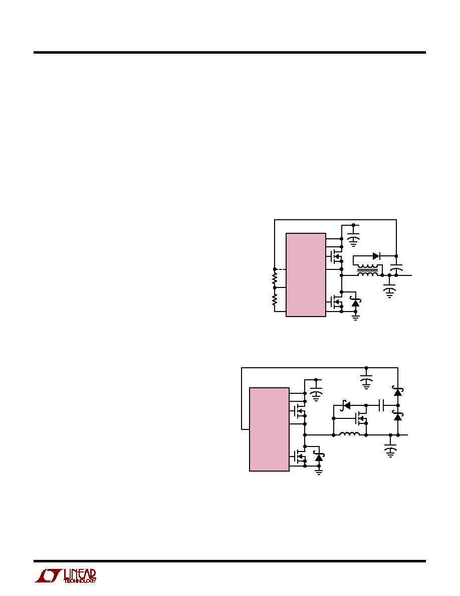
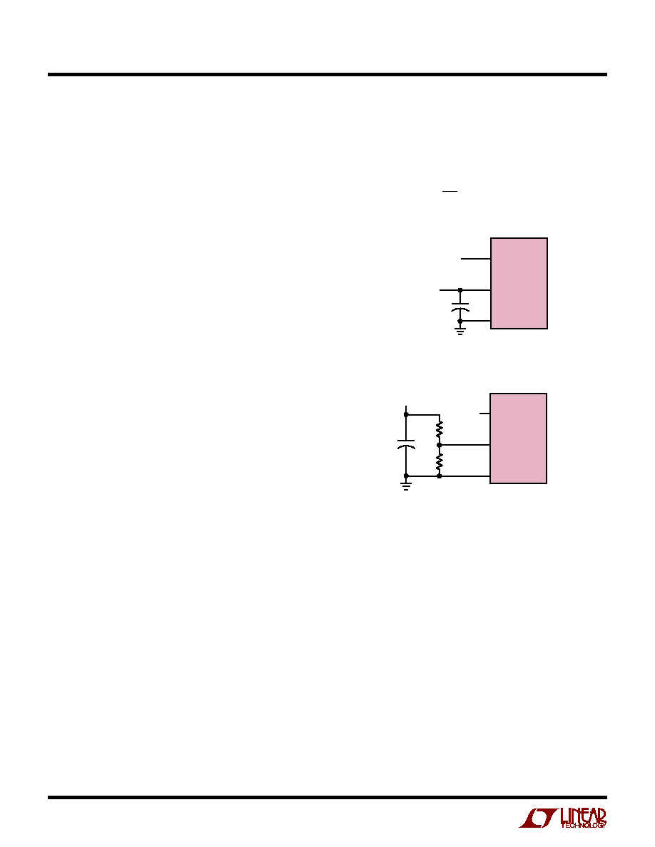
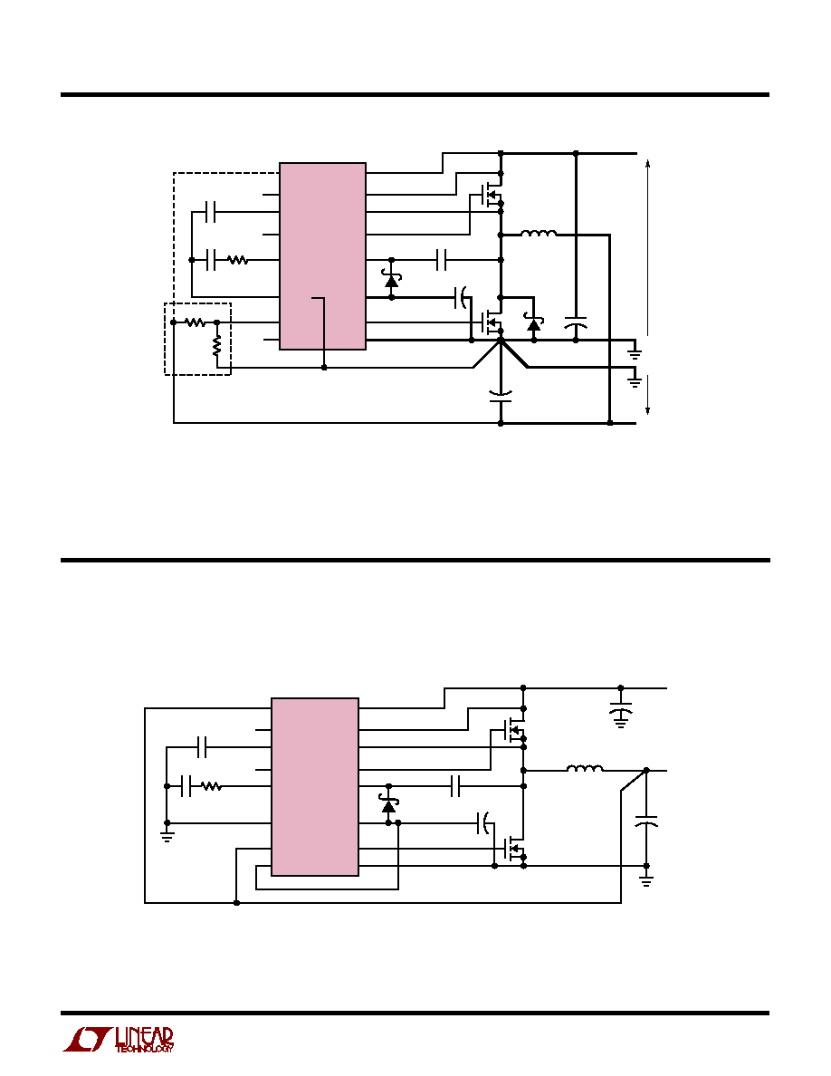
inductive boost winding as shown in Figure 5a or a
capacitive charge pump as shown in Figure 5b.
4. EXTV
CC
connected to an external supply. If an external
supply is available in the 5V to 7V range (EXTV
CC
< V
IN
),
it may be used to power EXTV
CC
providing it is compat-
ible with the MOSFET gate drive requirements.
V
IN
TK
LTC1625
SGND
FCB
EXTV
CC
TG
SW
OPTIONAL
EXTV
CC
CONNECTION
5V < V
SEC
< 7V
R3
R4
1625 F05a
T1
1:N
BG
PGND
+
C
SEC
1
µ
F
V
OUT
V
SEC
V
IN
+
C
IN
1N4148
∑
∑
+
C
OUT
Figure 5a: Secondary Output Loop and EXTV
CC
Connection
V
IN
TK
LTC1625
EXTV
CC
V
PUMP
2(V
OUT
≠ V
D
)
TG
SW
1625 F05b
L1
BG
PGND
+
C
OUT
V
OUT
BAT85
BAT85
BAT85
VN2222LL
V
IN
+
C
IN
+
1
µ
F
0.22
µ
F
Figure 5b: Capacitive Charge Pump for EXTV
CC
14
LTC1625
Note that R
DS(ON)
also varies with the gate drive level. If
gate drives other than the 5.2V INTV
CC
are used, this must
be accounted for when selecting the MOSFET R
DS(ON)
.
Particular care should be taken with applications where
EXTV
CC
is connected to the output. When the output
voltage is between 4.7V and 5.2V, INTV
CC
will be con-
nected to the output and the gate drive is reduced. The
resulting increase in R
DS(ON)
will also lower the current
limit. Even applications with V
OUT
> 5.2V will traverse this
region during start-up and must take into account the
reduced current limit.
Topside MOSFET Driver Supply (C
B
, D
B
)
An external bootstrap capacitor (C
B
in the functional
diagram) connected to the BOOST pin supplies the gate
drive voltage for the topside MOSFET. This capacitor is
charged through diode D
B
from INTV
CC
when the SW node
is low. Note that the voltage across C
B
is about a diode
drop below INTV
CC
. When the top MOSFET turns on, the
switch node voltage rises to V
IN
and the BOOST pin rises
to approximately V
IN
+ INTV
CC
. During dropout operation,
C
B
supplies the top driver for as long as ten cycles between
refreshes. Thus, the boost capacitance needs to store
about 100 times the gate charge required by the top
MOSFET. In many applications 0.22
µ
F is adequate.
When adjusting the gate drive level , the final arbiter is the
total input current for the regulator. If you make a change
and the input current decreases, then you improved the
efficiency. If there is no change in input current, then there
is no change in efficiency.
Output Voltage Programming
The LTC1625 has a pin selectable output voltage deter-
mined by the V
PROG
pin as follows:
V
PROG
= 0V
V
OUT
= 3.3V
V
PROG
= INTV
CC
V
OUT
= 5V
V
PROG
= Open
V
OUT
= Adjustable
Remote sensing of the output voltage is provided by the
V
OSENSE
pin. For fixed 3.3V and 5V output applications an
internal resistive divider is used and the V
OSENSE
pin is
connected directly to the output voltage as shown in
Figure 6a. When using an external resistive divider, the
APPLICATIO
N
S I
N
FOR
M
ATIO
N
W
U
U
U
V
PROG
pin is left open and the V
OSENSE
pin is connected to
feedback resistors as shown in Figure 6b. The output
voltage is set by the divider as:
V
V
R
R
OUT
=
+
1 19
1
2
1
.
V
PROG
V
OUT
= 5V: INTV
CC
V
OUT
= 3.3V: GND
LTC1625
V
OSENSE
1625 F06a
SGND
C
OUT
V
OUT
+
Figure 6a. Fixed 3.3V or 5V V
OUT
V
PROG
OPEN
LTC1625
V
OSENSE
1625 F06b
SGND
C
OUT
R1
R2
+
Figure 6b. Adjustable V
OUT
Run/Soft Start Function
The RUN/SS pin is a dual purpose pin that provides a soft
start function and a means to shut down the LTC1625. Soft
start reduces surge currents from V
IN
by gradually in-
creasing the controller's current limit I
TH(MAX)
. This pin
can also be used for power supply sequencing.
Pulling the RUN/SS pin below 1.4V puts the LTC1625 into
a low quiescent current shutdown (I
Q
< 30
µ
A). This pin can
be driven directly from logic as shown in Figure 7. Releas-
ing the RUN/SS pin allows an internal 3
µ
A current source
to charge up the external capacitor C
SS
. If RUN/SS has
been pulled all the way to ground there is a delay before
starting of approximately:
15
LTC1625
then V
SEC
will droop. An external resistor divider from
V
SEC
to the FCB pin sets a minimum voltage V
SEC(MIN)
:
V
V
R
R
SEC MIN
(
)
.
+
1 19
1
4
3
If V
SEC
drops below this level, the FCB voltage forces
continuous operation until V
SEC
is again above its
minimum.
Minimum On-Time Considerations
Minimum on-time t
ON(MIN)
is the smallest amount of time
that the LTC1625 is capable of turning the top MOSFET on
and off again. It is determined by internal timing delays and
the amount of gate charge required to turn on the top
MOSFET. Low duty cycle applications may approach this
minimum on-time limit and care should be taken to ensure
that:
t
V
V
f
ON MIN
OUT
IN
(
)
(
)( )
<
If the duty cycle falls below what can be accommodated by
the minimum on-time, the LTC1625 will begin to skip
cycles. The output voltage will continue to be regulated,
but the ripple current and ripple voltage will increase.
The minimum on-time for the LTC1625 is generally about
0.5
µ
s. However, as the peak sense voltage (I
L(PEAK) ∑
R
DS(ON)
) decreases, the minimum on-time gradually
increases up to about 0.7
µ
s. This is of particular concern
in forced continuous applications with low ripple current
at light loads. If the duty cycle drops below the minimum
on-time limit in this situation, a significant amount of
cycle skipping can occur with correspondingly larger
current and voltage ripple.
Efficiency Considerations
The efficiency of a switching regulator is equal to the
output power divided by the input power (
◊
100%). Per-
cent efficiency can be expressed as:
%Efficiency = 100% ≠ (L1 + L2 + L3 + ...)
APPLICATIO
N
S I
N
FOR
M
ATIO
N
W
U
U
U
t
V
A
C
s
F C
DELAY
SS
SS
=
µ
=
µ
(
)
1 4
3
0 5
.
.
/
When the voltage on RUN/SS reaches 1.4V the LTC1625
begins operating with a clamp on I
TH
at 0.8V. As the
voltage on RUN/SS increases to approximately 3.1V, the
clamp on I
TH
is raised until its full 2.4V range is restored.
This takes an additional 0.5s/
µ
F. During this time the load
current will be folded back to approximately 30mV/R
DS(ON)
until the output reaches half of its final value.
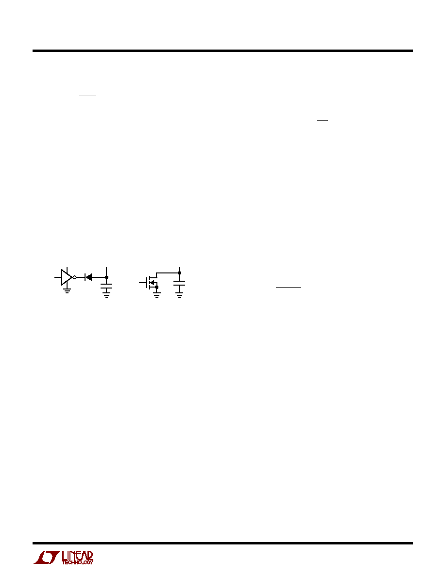
Diode D1 in Figure 7 reduces the start delay while allowing
C
SS
to charge up slowly for the soft start function. This
diode and C
SS
can be deleted if soft start is not needed. The
RUN/SS pin has an internal 6V zener clamp (See Func-
tional Diagram).
3.3V
OR 5V
RUN/SS
D1
C
SS
1625 F07
RUN/SS
C
SS
Figure 7. RUN/SS Pin Interfacing
FCB Pin Operation
When the FCB pin drops below its 1.19V threshold,
continuous synchronous operation is forced. In this case,
the top and bottom MOSFETs continue to be driven
regardless of the load on the main output. Burst Mode
operation is disabled and current reversal is allowed in the
inductor.
In addition to providing a logic input to force continuous
operation, the FCB pin provides a means to regulate a
flyback winding output. It can force continuous synchro-
nous operation when needed by the flyback winding,
regardless of the primary output load.
The secondary output voltage V
SEC
is normally set as
shown in Figure 5a by the turns ratio N of the transformer:
V
SEC
(N + 1)V
OUT
However, if the controller goes into Burst Mode operation
and halts switching due to a light primary load current,

16
LTC1625
where L1, L2, etc. are the individual losses as a percentage
of input power. It is often useful to analyze individual
losses to determine what is limiting the efficiency and
which change would produce the most improvement.
Although all dissipative elements in the circuit produce
losses, four main sources usually account for most of the
losses in LTC1625 circuits:
1. INTV
CC
current. This is the sum of the MOSFET driver
and control currents. The driver current results from
switching the gate capacitance of the power MOSFETs.
Each time a MOSFET gate is switched on and then off,
a packet of gate charge Q
g
moves from INTV
CC
to
ground. The resulting current out of INTV
CC
is typically
much larger than the control circuit current. In continu-
ous mode, I
GATECHG
= f(Q
g(TOP)
+ Q
g(BOT)
).
By powering EXTV
CC
from an output-derived source,
the additional V
IN
current resulting from the driver and
control currents will be scaled by a factor of Duty Cycle/
Efficiency. For example, in a 20V to 5V application at
400mA load, 10mA of INTV
CC
current results in ap-
proximately 3mA of V
IN
current. This reduces the loss
from 10% (if the driver was powered directly from V
IN
)
to about 3%.
2. DC I
2
R Losses. Since there is no separate sense resis-
tor, DC I
2
R losses arise only from the resistances of the
MOSFETs and inductor. In continuous mode the aver-
age output current flows through L, but is "chopped"
between the top MOSFET and the bottom MOSFET. If
the two MOSFETs have approximately the same R
DS(ON)
,
then the resistance of one MOSFET can simply be
summed with the resistance of L to obtain the DC I
2
R
loss. For example, if each R
DS(ON)
= 0.05
and R
L
=
0.15
, then the total resistance is 0.2
. This results in
losses ranging from 2% to 8% as the output current
increases from 0.5A to 2A for a 5V output. I
2
R losses
cause the efficiency to drop at high output currents.
3. Transition losses apply only to the topside MOSFET,
and only when operating at high input voltages (typi-
cally 20V or greater). Transition losses can be esti-
mated from:
Transition Loss = (1.7)(V
IN
2
)(I
O(MAX)
)(C
RSS
)(f)
APPLICATIO
N
S I
N
FOR
M
ATIO
N
W
U
U
U
4. LTC1625 V
IN
supply current. The V
IN
current is the DC
supply current to the controller excluding MOSFET gate
drive current. Total supply current is typically about
850
µ
A. If EXTV
CC
is connected to 5V, the LTC1625 will
draw only 330
µ
A from V
IN
and the remaining 520
µ
A will
come from EXTV
CC
. V
IN
current results in a small
(< 1%) loss which increases with V
IN
.
Other losses including C
IN
and C
OUT
ESR dissipative
losses, Schottky conduction losses during dead time
and inductor core losses, generally account for less
than 2% total additional loss.
Checking Transient Response
The regulator loop response can be checked by looking at
the load transient response. Switching regulators take
several cycles to respond to a step in DC (resistive) load
current. When a load step occurs, V
OUT
immediately shifts
by an amount equal to (
I
LOAD
)(ESR), where ESR is the
effective series resistance of C
OUT
, and C
OUT
begins to
charge or discharge. The regulator loop acts on the
resulting feedback error signal to return V
OUT
to its steady-
state value. During this recovery time V
OUT
can be moni-
tored for overshoot or ringing which would indicate a
stability problem. The I
TH
pin external components shown
in Figure 1 will provide adequate compensation for most
applications.
A second, more severe transient is caused by connecting
loads with large (> 1
µ
F) supply bypass capacitors. The
discharged bypass capacitors are effectively put in parallel
with C
OUT
, causing a rapid drop in V
OUT
. No regulator can
deliver enough current to prevent this problem if the load
switch resistance is low and it is driven quickly. The only
solution is to limit the rise time of the switch drive in order
to limit the inrush current to the load.
Automotive Considerations: Plugging into the
Cigarette Lighter
As battery-powered devices go mobile, there is a natural
interest in plugging into the cigarette lighter in order to
conserve or even recharge battery packs during opera-
tion. But before you connect, be advised: you are plug-
ging into the supply from hell. The main battery line in an
17
LTC1625
APPLICATIO
N
S I
N
FOR
M
ATIO
N
W
U
U
U
automobile is the source of a number of nasty potential
transients, including load dump, reverse and double
battery.
Load dump is the result of a loose battery cable. When the
cable breaks connection, the field collapse in the alternator
can cause a positive spike as high as 60V which takes
several hundred milliseconds to decay. Reverse battery is
just what it says, while double battery is a consequence of
tow truck operators finding that a 24V jump start cranks
cold engines faster than 12V.
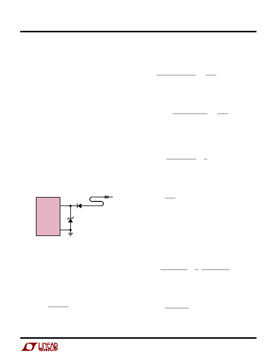
The network shown in Figure 8 is the most straightforward
approach to protect a DC/DC converter from the ravages
of an automotive battery line. The series diode prevents
current from flowing during reverse battery, while the
transient suppressor clamps the input voltage during load
dump. Note that the transient suppressor should not
conduct during double-battery operation, but must still
clamp the input voltage below breakdown of the converter.
Although the LTC1625 has a maximum input voltage of
36V, most applications will be limited to 30V by the
MOSFET V
(BR)DSS
.
For 40% ripple current at maximum V
IN
the inductor
should be:
L
V
kHz
A
V
V
H
= µ
3 3
225
0 4 2
1
3 3
22
16
.
(
)( . )(
)
≠
.
Choosing a standard value of 15
µ
H results in a maximum
ripple current of:
I
V
kHz
H
V
V
A
L MAX
(
)
.
(
)(
)
≠
.
.
=
µ
=
3 3
225
15
1
3 3
22
0 83
Next, check that the minimum value of the current limit is
acceptable. Assume a junction temperature close to a
70
∞
C ambient with
80
∞
C
= 1.3.
I
mV
A
A
LIMIT
=
150
0 042
1 3
1
2
0 83
2 3
( .
)( . )
≠
.
.
This is comfortably above I
O(MAX)
= 2A. Now double-check
the assumed T
J
:
P
V
V
A
A
pF
kHz
mW
mW
mW
TOP
=
+
=
+
=
3 3
22
2 3
1 3 0 042
1 7 22
2 3
180
225
43
77
120
2
2
.
( .
) ( . )( .
)
( . )(
) ( .
)(
)(
)
T
J
= 70
∞
C + (120mW)(50
∞
C/W) = 76
∞
C
Since
(76
∞
C)
(80
∞
C), the solution is self-consistent.
A short circuit to ground will result in a folded back
current of:
I
mV
V
s
H
A
SC
=
+
µ
µ
=
30
0 03
1 1
1
2
15
0 5
15
1 2
( .
)( . )
(
)( .
)
.
with a typical value of R
DS(ON)
and
(50
∞
C) = 1.1. The
resulting power dissipated in the bottom MOSFET is:
P
V
V
V
A
mW
BOT
=
=
15
3 3
15
1 2
1 1 0 03
37
2
≠ .
( .
) ( . )( .
)
which is less than under full load conditions.
V
IN
TRANSIENT VOLTAGE
SUPPRESSOR
GENERAL INSTRUMENT
1.5KA24A
12V
LTC1625
50A I
PK
RATING
1625 F08
PGND
Figure 8. Automotive Application Protection
Design Example
As a design example, take a supply with the following
specifications: V
IN
= 12V to 22V (15V nominal), V
OUT
=
3.3V, I
O(MAX)
= 2A, and f = 225kHz. The required R
DS(ON)
can immediately be estimated:
R
mV
A
DS ON
(
)
(
)( . )
.
=
=
120
2
1 3
0 046
A 0.042
Siliconix Si4412DY MOSFET (
JA
= 50
∞
C/W) is
close to this value.
18
LTC1625
APPLICATIO
N
S I
N
FOR
M
ATIO
N
W
U
U
U
+
C
SS
0.1
µ
F
R
C
10k
C
C1
470pF
C
C2
220pF
M1
Si4412DY
C
IN
22
µ
F
35V
◊
2
V
IN
12V TO 22V
V
OUT
3.3V
2A
M2
Si4412DY
D1
MBRS140T3
D
B
CMDSH-3
C
VCC
4.7
µ
F
1625 F09
OPEN
INTV
CC
V
IN
TK
EXTV
CC
LTC1625
SYNC
V
PROG
SW
TG
BOOST
INTV
CC
BG
RUN/SS
FCB
I
TH
SGND
V
OSENSE
PGND
1
2
3
4
5
6
7
8
16
15
14
13
12
11
10
9
C
B
0.1
µ
F
L1
15
µ
H
+
C
OUT
100
µ
F
10V
0.065
◊
2
+
C
IN
: AVX TPSE226M035R0300
C
OUT
: AVX TPSD107M010R0065
L1: SUMIDA CDRH125-150MC
Figure 9. 3.3V/2A Fixed Output at 225kHz
C
IN
is chosen for an RMS current rating of at least 1A at
temperature. C
OUT
is chosen with an ESR of 0.033
for
low output ripple. The output ripple in continuous mode
will be highest at the maximum input voltage and is
approximately:
V
O
= (
I
L(MAX)
)(ESR) = (0.83A)(0.033
) = 27mV
The complete circuit is shown in Figure 9.
PC Board Layout Checklist
When laying out the printed circuit board, the following
checklist should be used to ensure proper operation of the
LTC1625. These items are also illustrated graphically in
the layout diagram of Figure 10. Check the following in
your layout:
1) Connect the TK lead directly to the drain of the topside
MOSFET. Then connect the drain to the (+) plate of C
IN
.
This capacitor provides the AC current to the top
MOSFET.
2) The power ground pin connects directly to the source of
the bottom N-channel MOSFET. Then connect the source
to the anode of the Schottky diode and (≠) plate of C
IN
,
which should have as short lead lengths as possible.
3) The LTC1625 signal ground pin must return to the (≠)
plate of C
OUT
. Connect the (≠) plate of C
OUT
to power
ground at the source of the bottom MOSFET
4) Keep the switch node SW away from sensitive small-
signal nodes. Ideally the switch node should be placed
on the opposite side of the power MOSFETs from the
LTC1625.
5) Connect the INTV
CC
decoupling capacitor C
VCC
closely
to the INTV
CC
pin and the power ground pin. This
capacitor carries the MOSFET gate drive current.
6) Does the V
OSENSE
pin connect directly to the (+) plate of
C
OUT
? In adjustable applications, the resistive divider
(R1, R2) must be connected between the (+) plate of
C
OUT
and signal ground. Place the divider near the
LTC1625 in order to keep the high impedance V
OSENSE
node short.
7) For applications with multiple switching power con-
verters connected to the same V
IN
, ensure that the input
filter capacitance for the LTC1625 is not shared with the
other converters. AC input current from another con-
verter will cause substantial input voltage ripple that
may interfere with proper operation of the LTC1625. A
few inches of PC trace or wire (
100nH) between C
IN
and V
IN
is sufficient to prevent sharing.
19
LTC1625
APPLICATIO
N
S I
N
FOR
M
ATIO
N
W
U
U
U
+
+
C
SS
OPTIONAL 5V EXTV
CC
CONNECTION
M1
M2
D1
C
VCC
BOLD LINES INDICATE HIGH CURRENT PATHS
1625 F10
C
IN
C
OUT
V
IN
V
OUT
OPEN
OPEN
EXT
CLK
R1
OUTPUT DIVIDER
REQUIRED
WITH V
PROG
OPEN
R2
C
C1
R
C
C
B
D
B
+
L1
+
+
≠
≠
V
IN
TK
EXTV
CC
LTC1625
SYNC
V
PROG
SW
TG
BOOST
INTV
CC
BG
RUN/SS
FCB
I
TH
SGND
V
OSENSE
PGND
2
1
3
4
5
6
7
8
16
15
14
13
12
11
10
9
Figure 10. LTC1625 Layout Diagram
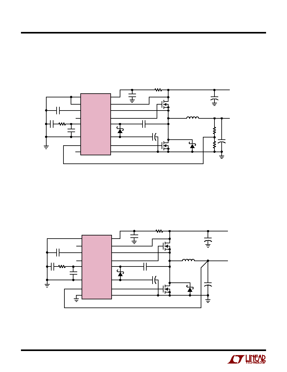
TYPICAL APPLICATIO
N
S
U
+
C
SS
0.1
µ
F
R
C
10k
C
C
330pF
C
IN
15
µ
F
35V
V
IN
5V TO 28V
V
OUT
5V
1.2A
M2
1/2 Si9936DY
M1
1/2 Si9936DY
C
VCC
4.7
µ
F
1625 TA02
OPEN
INTV
CC
C
B
0.1
µ
F
D
B
CMDSH-3
L1
39
µ
H
C
IN
: AVX TPSD156M035R0300
C
OUT
: AVX TPSD107M010R0100
L1: SUMIDA CD104-390MC
+
C
OUT
100
µ
F
10V
0.100
+
V
IN
TK
EXTV
CC
LTC1625
SYNC
V
PROG
SW
TG
BOOST
INTV
CC
BG
RUN/SS
FCB
I
TH
SGND
V
OSENSE
PGND
1
2
3
4
5
6
7
8
16
15
14
13
12
11
10
9
5V/1.2A Fixed Output at 225kHz
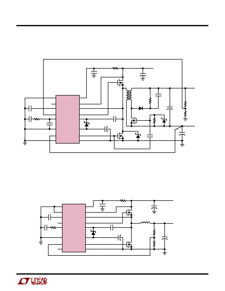
20
LTC1625
TYPICAL APPLICATIO
N
S
U
+
C
SS
0.1
µ
F
R
C
10k
C
C1
2.2nF
C
C2
220pF
C
IN
10
µ
F
30V
◊
3
C
F
0.1
µ
F
V
IN
5V TO 28V
V
OUT
3.3V
7A
M2
FDS6680A
D1
MBRS140T3
M1
FDS6680A
C
VCC
4.7
µ
F
1625 TA05
OPEN
EXT
CLK
C
IN
: SANYO 30SC10M
C
OUT
: SANYO 6SA150M
C
B
0.22
µ
F
D
B
CMDSH-3
L1
7
µ
H
+
C
OUT
150
µ
F
6.3V
0.03
◊
2
+
R
F
4.7
V
IN
TK
EXTV
CC
LTC1625
SYNC
V
PROG
SW
TG
BOOST
INTV
CC
BG
RUN/SS
FCB
I
TH
SGND
V
OSENSE
PGND
1
2
3
4
5
6
7
8
16
15
14
13
12
11
10
9
2.5V/2.8A Adjustable Output
+
C
SS
0.1
µ
F
R
C
10k
C
C1
1nF
C
C2
330pF
C
IN
22
µ
F
35V
◊
2
V
IN
5V TO 28V
V
OUT
2.5V
2.8A
M2
1/2 Si4920DY
D1
MBRS140T3
M1
1/2 Si4920DY
C
VCC
4.7
µ
F
1625 TA03
OPEN
OPEN
C
B
0.22
µ
F
D
B
CMDSH-3
L1
15
µ
H
R2
11k
1%
C
IN
: AVX TPSE226M020R0300
C
OUT
: AVX TPSD107M010R0065
L1: SUMIDA CDRH125-150MC
+
C
F
0.1
µ
F
R
F
4.7
C
OUT
100
µ
F
10V
0.065
◊
2
+
R1
10k
1%
V
IN
TK
EXTV
CC
LTC1625
SYNC
V
PROG
SW
TG
BOOST
INTV
CC
BG
RUN/SS
FCB
I
TH
SGND
V
OSENSE
PGND
1
2
3
4
5
6
7
8
16
15
14
13
12
11
10
9
3.3V/7A Fixed Output
21
LTC1625
TYPICAL APPLICATIO
N
S
U
3.3V/4A Fixed Output with 12V/120mA Auxiliary Output
+
C
SS
0.1
µ
F
R
C
10k
C
C1
470pF
C
C2
220pF
M2
IRLR3103
C
IN
: SANYO 30SC10M
C
OUT
: AVX TPSD107M010R0065
C
SEC
: AVX TAJB335M035R
T1: BH ELECTRONICS 510-1079
*YES! USE A STANDARD RECOVERY DIODE
D1
MBRS140T3
M1
IRLR3103
C
VCC
4.7
µ
F
1625 TA04
EXT
CLK
C
B
0.22
µ
F
D
B
CMDSH-3
R
F
4.7
C
F
0.1
µ
F
C
IN
10
µ
F
30V
◊
2
V
IN
6V TO 20V
C
SEC
3.3
µ
F
35V
C1
0.01
µ
F
M3
NDT410EL
D
S
SM4003TR*
D2
CDMSH-3
T1
8
µ
H
1:2.53
R1
4.7k
R4
95.3k
1%
R3
11k
1%
+
+
C
OUT
100
µ
F
10V
0.065
◊
3
V
SEC
12V
120mA
V
OUT
3.3V
4A
+
R
S
100k
∑
∑
C
S
0.1
µ
F
V
IN
TK
EXTV
CC
LTC1625
SYNC
V
PROG
SW
TG
BOOST
INTV
CC
BG
RUN/SS
FCB
I
TH
SGND
V
OSENSE
PGND
1
2
3
4
5
6
7
8
16
15
14
13
12
11
10
9
12V/2.2A Adjustable Output
+
C
IN
: AVX TPSE226M020R0300
C
OUT
: AVX TPSE686M020R0150
L1: SUMIDA CDRH127-270MC
C
SS
0.1
µ
F
R
C
22k
C
C
470pF
C
IN
22
µ
F
35V
◊
2
V
IN
12.5V TO 28V
V
OUT
12V
2A
R2
35.7k
1%
R1
3.92k
1%
M2
Si4412DY
M1
Si4412DY
C
VCC
4.7
µ
F
1625TA06
OPEN
C
B
0.1
µ
F
D
B
CMDSH-3
L1
27
µ
H
+
C
OUT
68
µ
F
20V
0.15
◊
2
+
V
IN
TK
EXTV
CC
LTC1625
SYNC
V
PROG
SW
TG
BOOST
INTV
CC
BG
RUN/SS
FCB
I
TH
SGND
V
OSENSE
PGND
1
2
3
4
5
6
7
8
16
15
14
13
12
11
10
9
C
F
0.1
µ
F
R
F
4.7
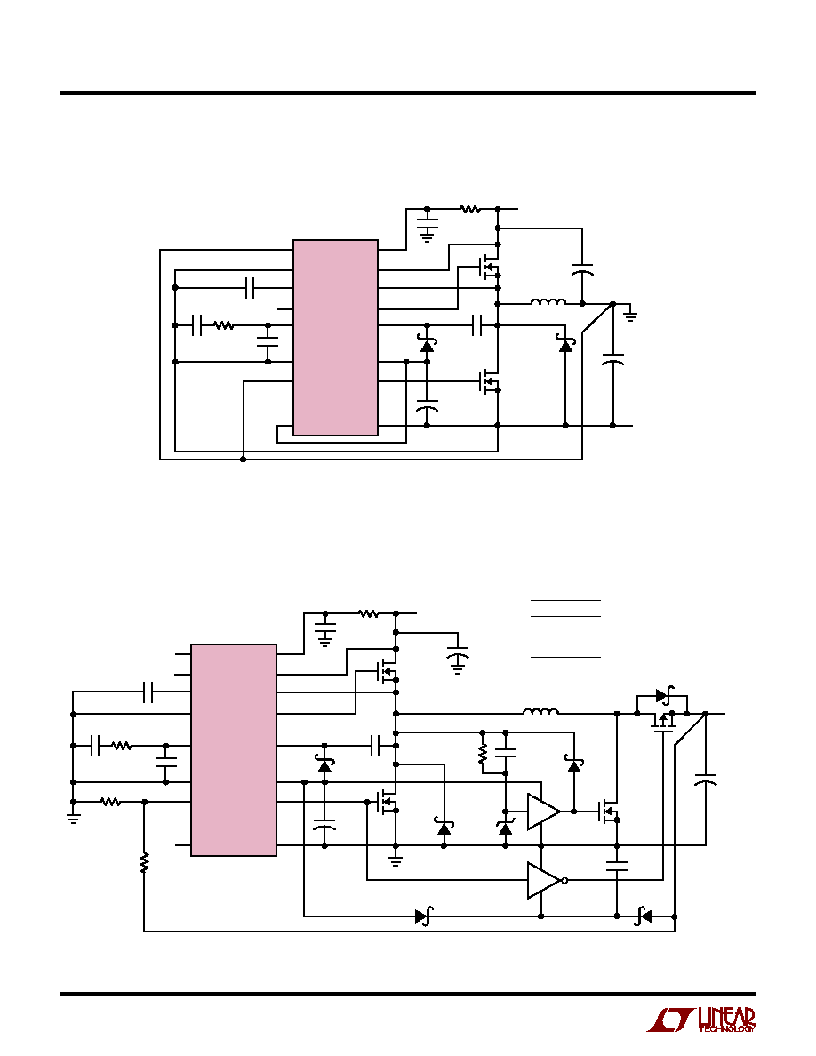
22
LTC1625
TYPICAL APPLICATIO
N
S
U
≠ 5V/4.5A Positive to Negative Converter
C
IN
: SANYO 16SV220M
C
OUT
: SANYO 6SV470M
L1: MAGNETICS Kool-M
µ
77120-A7, 9 TURNS, 17 GAUGE
C
SS
0.1
µ
F
R
C
10k
C
C1
2.2nF
V
IN
5V TO 10V
V
OUT
≠5V
4.5A
1625TA08
D
B
CMDSH-3
M2
FDS6670A
L1
6
µ
H
C
VCC
4.7
µ
F
C
IN
220
µ
F
16V
+
+
C
OUT
470
µ
F
6.3V
+
D
1
MBR140T3
V
IN
TK
EXTV
CC
LTC1625
SYNC
V
PROG
SW
TG
BOOST
INTV
CC
BG
RUN/SS
FCB
I
TH
SGND
V
OSENSE
PGND
1
2
3
4
5
6
7
8
16
15
14
13
12
11
10
9
C
C2
220pF
C
F
0.1
µ
F
M1
FDS6670A
C
B
0.22
µ
F
R
F
4.7
C
IN
: SANYO 20S68M
C
OUT
: SANYO 16SA100M
L1: 7A, 18
µ
H Kool-M
µ
77120-A7, 15 TURNS, 17 GAUGE
C
SS
0.1
µ
F
R
C
10k
C
C1
2.2nF
V
IN
6V TO 18V
V
OUT
12V
1625TA09
D
B
CMDSH-3
D4
BAT85
L1
18
µ
H
C
VCC
4.7
µ
F
C
IN
68
µ
F
20V
x2
+
+
C
OUT
100
µ
F
16V
30m
x2
+
D2
MBRS340T3
D5
BAT85
D1
MBRS
340T3
Z1
MMBZ
5240
10V
V
IN
TK
EXTV
CC
LTC1625
SYNC
V
PROG
SW
TG
BOOST
INTV
CC
BG
RUN/SS
FCB
I
TH
SGND
V
OSENSE
PGND
1
2
3
4
5
6
7
8
16
15
14
13
12
11
10
9
C
C2
220pF
C
F
0.1
µ
F
M1
Si4420DY
M2
Si4420DY
M3
Si4420DY
M4
Si4425DY
C
B
0.33
µ
F
R
F
4.7
R1
3.92k
R2
35.7k
R1
100k
4
6
5
3
8
2
1
7
C1
470pF
C2
0.1
µ
F
D3
BAT85
1/2
LTC1693-2
1/2
LTC1693-2
V
IN
18
12
6
I
OUT
4.0
3.3
2.0
Single Inductor, Positive Output Buck Boost
23
LTC1625
PACKAGE DESCRIPTIO
N
U
Dimensions in inches (millimeters) unless otherwise noted.
0.016 ≠ 0.050
0.406 ≠ 1.270
0.010 ≠ 0.020
(0.254 ≠ 0.508)
◊
45
∞
0
∞
≠ 8
∞
TYP
0.008 ≠ 0.010
(0.203 ≠ 0.254)
1
2
3
4
5
6
7
8
0.150 ≠ 0.157**
(3.810 ≠ 3.988)
16
15
14
13
0.386 ≠ 0.394*
(9.804 ≠ 10.008)
0.228 ≠ 0.244
(5.791 ≠ 6.197)
12
11
10
9
S16 0695
0.053 ≠ 0.069
(1.346 ≠ 1.752)
0.014 ≠ 0.019
(0.355 ≠ 0.483)
0.004 ≠ 0.010
(0.101 ≠ 0.254)
0.050
(1.270)
TYP
DIMENSION DOES NOT INCLUDE MOLD FLASH. MOLD FLASH
SHALL NOT EXCEED 0.006" (0.152mm) PER SIDE
DIMENSION DOES NOT INCLUDE INTERLEAD FLASH. INTERLEAD
FLASH SHALL NOT EXCEED 0.010" (0.254mm) PER SIDE
*
**
S Package
16-Lead Plastic Small Outline (Narrow 0.150)
(LTC DWG # 05-08-1610)
GN Package
16-Lead Plastic SSOP (Narrow 0.150)
(LTC DWG # 05-08-1641)
GN16 (SSOP) 0398
* DIMENSION DOES NOT INCLUDE MOLD FLASH. MOLD FLASH
SHALL NOT EXCEED 0.006" (0.152mm) PER SIDE
** DIMENSION DOES NOT INCLUDE INTERLEAD FLASH. INTERLEAD
FLASH SHALL NOT EXCEED 0.010" (0.254mm) PER SIDE
1
2
3
4
5
6
7
8
0.229 ≠ 0.244
(5.817 ≠ 6.198)
0.150 ≠ 0.157**
(3.810 ≠ 3.988)
16 15 14 13
0.189 ≠ 0.196*
(4.801 ≠ 4.978)
12 11 10 9
0.016 ≠ 0.050
(0.406 ≠ 1.270)
0.015
±
0.004
(0.38
±
0.10)
◊
45
∞
0
∞
≠ 8
∞
TYP
0.007 ≠ 0.0098
(0.178 ≠ 0.249)
0.053 ≠ 0.068
(1.351 ≠ 1.727)
0.008 ≠ 0.012
(0.203 ≠ 0.305)
0.004 ≠ 0.0098
(0.102 ≠ 0.249)
0.025
(0.635)
BSC
0.009
(0.229)
REF
Information furnished by Linear Technology Corporation is believed to be accurate and reliable.
However, no responsibility is assumed for its use. Linear Technology Corporation makes no represen-
tation that the interconnection of its circuits as described herein will not infringe on existing patent rights.

24
LTC1625
©
LINEAR TECHNOLOGY CORPORATION 1998
1625f LT/TP 1298 4K ∑ PRINTED IN USA
PART NUMBER
DESCRIPTION
COMMENTS
LTC1435A
High Efficiency Synchronous Step-Down Controller
Optimized for Low Duty Cycle Battery to CPU Power Applications
LTC1436A-PLL
High Efficiency Low Noise Synchronous Step-Down Controller
PLL Synchronization and Auxiliary Linear Regulator
LTC1438
Dual High Efficiency Step-Down Controller
Power-On Reset and Low-Battery Comparator
LTC1530
High Power Synchronous Step-Down Controller
SO-8 with Current Limit, No R
SENSE
Saves Space, Fixed
Frequency Ideal for 5V to 3.3V
LTC1538-AUX
Dual High Efficiency Step-Down Controller
5V Standby Output and Auxiliary Linear Regulator
LTC1649
3.3V Input High Power Step-Down Controller
2.7V to 5V Input, 90% Efficiency, Ideal for 3.3V to 1.xV ≠ 2.xV
Up to 20A
RELATED PARTS
Linear Technology Corporation
1630 McCarthy Blvd., Milpitas, CA 95035-7417
(408) 432-1900
q
FAX: (408) 434-0507
q
www.linear-tech.com
3.3V/1.8A Fixed Output
+
C
IN
: AVX TPSD156M035R0300
C
OUT
: AVX TPSD107M010R0100
L1: SUMIDA CDRH125-270MC
C
SS
0.1
µ
F
R
C
10k
C
C1
1nF
C
C2
100pF
C
IN
15
µ
F
35V
◊
2
V
IN
5V TO 28V
V
OUT
3.3V
1.8A
M2
1/2 Si4936DY
D1
MBRS140T3
M1
1/2 Si4936DY
C
VCC
4.7
µ
F
1625 TA07
OPEN
C
B
0.1
µ
F
D
B
CMDSH-3
L1
27
µ
H
+
C
OUT
100
µ
F
10V
0.1
◊
2
+
V
IN
TK
EXTV
CC
LTC1625
SYNC
V
PROG
SW
TG
BOOST
INTV
CC
BG
RUN/SS
FCB
I
TH
SGND
V
OSENSE
PGND
1
2
3
4
5
6
7
8
16
15
14
13
12
11
10
9
TYPICAL APPLICATIO
N
U