 | –≠–ª–µ–∫—Ç—Ä–æ–Ω–Ω—ã–π –∫–æ–º–ø–æ–Ω–µ–Ω—Ç: LTC1628C | –°–∫–∞—á–∞—Ç—å:  PDF PDF  ZIP ZIP |
1
LTC1628/LTC1628-PG
High Efficiency, 2-Phase
Synchronous Step-Down Switching Regulators
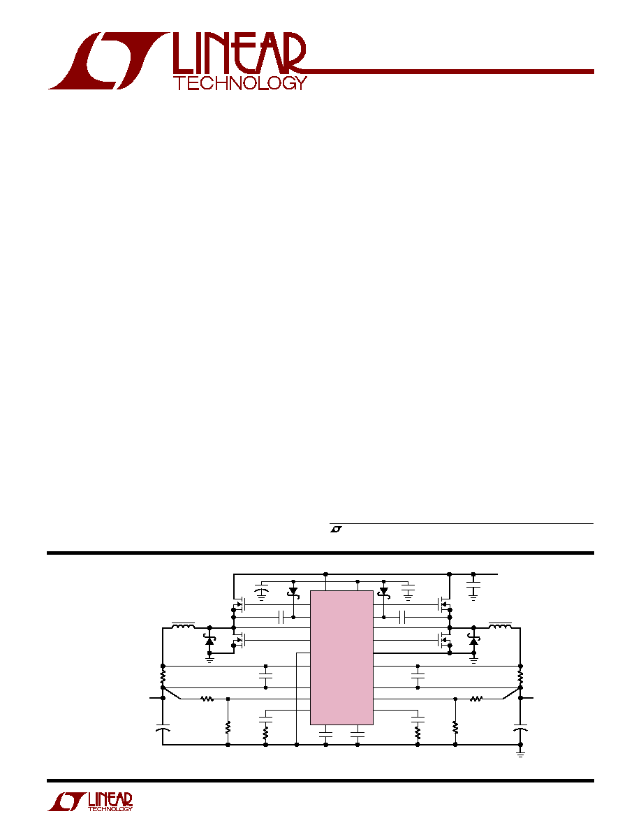
Figure 1. High Efficiency Dual 5V/3.3V Step-Down Converter
s
Out-of-Phase Controllers Reduce Required Input
Capacitance and Power Supply Induced Noise
s
OPTI-LOOP
TM
Compensation Minimizes C
OUT
s
Dual N-Channel MOSFET Synchronous Drive
s
±
1% Output Voltage Accuracy
s
Power Good Output Voltage Monitor (LTC1628-PG)
s
DC Programmed Fixed Frequency 150kHz to 300kHz
s
Wide V
IN
Range: 3.5V to 36V Operation
s
Very Low Dropout Operation: 99% Duty Cycle
s
Adjustable Soft-Start Current Ramping
s
Foldback Output Current Limiting
s
Latched Short-Circuit Shutdown with Defeat Option
s
Output Overvoltage Protection
s
Remote Output Voltage Sense
s
Low Shutdown I
Q
: 20
µ
A
s
5V and 3.3V Standby Regulators
s
Small 28-Lead SSOP Package
s
Selectable Constant Frequency or Burst Mode
TM
Operation
The LTC
Æ
1628/LTC1628-PG are high performance dual
step-down switching regulator controllers that drive all
N-channel synchronous power MOSFET stages. A con-
stant frequency current mode architecture allows adjust-
ment of the frequency up to 300kHz. Power loss and noise
due to the ESR of the input capacitors are minimized by
operating the two controller output stages out of phase.
OPTI-LOOP compensation allows the transient response
to be optimized over a wide range of output capacitance and
ESR values. The precision 0.8V reference and power good
output indicator are compatible with future microproces-
sor generations, and a wide 3.5V to 30V (36V maximum)
input supply range encompasses all battery chemistries.
A RUN/SS pin for each controller provides both soft-start
and optional timed, short-circuit shutdown. Current
foldback limits MOSFET dissipation during short-circuit
conditions when overcurrent latchoff is disabled. Output
overvoltage protection circuitry latches on the bottom
MOSFET until V
OUT
returns to normal. The FCB mode pin
can select among Burst Mode, constant frequency mode
and continuous inductor current mode or regulate a
secondary winding. The LTC1628-PG includes a power
good output pin that replaces the FLTCPL, fault coupling
control pin of the LTC1628.
s
Notebook and Palmtop Computers, PDAs
s
Battery Chargers
s
Portable Instruments
s
Battery-Operated Digital Devices
s
DC Power Distribution Systems
, LTC and LT are registered trademarks of Linear Technology Corporation.
Burst Mode and OPTI-LOOP are trademarks of Linear Technology Corporation.
DESCRIPTIO
U
FEATURES
APPLICATIO S
U
TYPICAL APPLICATIO
U
+
4.7
µ
F
D3
D4
D1
M2
M1
C
B1
, 0.1
µ
F
R2
105k
1%
1000pF
L1
6.3
µ
H
C
C1
220pF
1
µ
F
CERAMIC
C
IN
22
µ
F
50V
CERAMIC
+
C
OUT1
47
µ
F
6V
SP
R
SENSE1
0.01
R1
20k
1%
R
C1
15k
V
OUT1
5V
5A
D2
M4
M3
C
B2
, 0.1
µ
F
R4
63.4k
1%
L2
6.3
µ
H
C
C2
220pF
1000pF
+
C
OUT
56
µ
F
6V
SP
R
SENSE2
0.01
R3
20k
1%
R
C2
15k
V
OUT2
3.3V
5A
TG1
TG2
BOOST1
BOOST2
SW1
SW2
BG1
BG2
SGND
PGND
SENSE1
+
SENSE2
+
SENSE1
≠
SENSE2
≠
V
OSENSE1
V
OSENSE2
I
TH1
I
TH2
V
IN
INTV
CC
RUN/SS1
RUN/SS2
V
IN
5.2V TO 28V
M1, M2, M3, M4: FDS6680A
1628 F01
C
SS1
0.1
µ
F
C
SS2
0.1
µ
F
LTC1628
2
LTC1628/LTC1628-PG
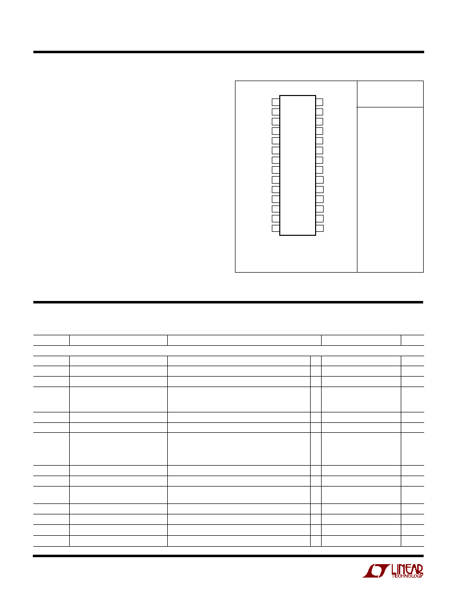
ORDER PART
NUMBER
LTC1628CG
LTC1628IG
LTC1628CG-PG
LTC1628IG-PG
(Note 1)
Input Supply Voltage (V
IN
).........................36V to ≠ 0.3V
Top Side Driver Voltages
(BOOST1, BOOST2) ...................................42V to ≠ 0.3V
Switch Voltage (SW1, SW2) .........................36V to ≠ 5V
INTV
CC,
EXTV
CC
, RUN/SS1, RUN/SS2, (BOOST1-SW1),
(BOOST2-SW2), PGOOD .............................7V to ≠ 0.3V
SENSE1
+
, SENSE2
+
, SENSE1
≠
,
SENSE2
≠
Voltages ........................ (1.1)INTV
CC
to ≠ 0.3V
FREQSET, STBYMD, FCB,
FLTCPL Voltage ................................... INTV
CC
to ≠ 0.3V
I
TH1,
I
TH2
, V
OSENSE1
, V
OSENSE2
Voltages ... 2.7V to ≠ 0.3V
Peak Output Current <10
µ
s (TG1, TG2, BG1, BG2) ... 3A
INTV
CC
Peak Output Current ................................ 50mA
Operating Temperature Range
LTC1628C/LTC1628C-PG ........................ 0
∞
C to 85
∞
C
LTC1628I/LTC1628I-PG ..................... ≠ 40
∞
C to 85
∞
C
Junction Temperature (Note 2) ............................. 125
∞
C
Storage Temperature Range ................. ≠ 65
∞
C to 150
∞
C
Lead Temperature (Soldering, 10 sec).................. 300
∞
C
T
JMAX
= 125
∞
C,
JA
= 95
∞
C/W
Consult factory for Military grade parts.
The
q
denotes the specifications which apply over the full operating
SYMBOL
PARAMETER
CONDITIONS
MIN
TYP
MAX
UNITS
Main Control Loops
V
OSENSE1, 2
Regulated Feedback Voltage
(Note 3); I
TH1, 2
Voltage = 1.2V
q
0.792
0.800
0.808
V
I
VOSENSE1, 2
Feedback Current
(Note 3)
≠ 5
≠ 50
nA
V
REFLNREG
Reference Voltage Line Regulation
V
IN
= 3.6V to 30V (Note 3)
0.002
0.02
%/V
V
LOADREG
Output Voltage Load Regulation
(Note 3)
Measured in Servo Loop;
I
TH
Voltage = 1.2V to 0.7V
q
0.1
0.5
%
Measured in Servo Loop;
I
TH
Voltage = 1.2V to 2.0V
q
≠ 0.1
≠ 0.5
%
g
m1, 2
Transconductance Amplifier g
m
I
TH1, 2
= 1.2V; Sink/Source 5uA; (Note 3)
1.3
mmho
g
mGBW1, 2
Transconductance Amplifier GBW
I
TH1, 2
= 1.2V; (Note 3)
3
MHz
I
Q
Input DC Supply Current
(Note 4)
Normal Mode
V
IN
= 15V; EXTV
CC
Tied to V
OUT1
; V
OUT1
= 5V
350
µ
A
Standby
V
RUN/SS1, 2
= 0V, V
STBYMD
> 2V
125
µ
A
Shutdown
V
RUN/SS1, 2
= 0V, V
STBYMD
= Open;
20
35
µ
A
V
FCB
Forced Continuous Threshold
q
0.76
0.800
0.84
V
I
FCB
Forced Continuous Pin Current
V
FCB
= 0.85V
≠ 0.30
≠ 0.18
≠ 0.1
µ
A
V
BINHIBIT
Burst Inhibit (Constant Frequency)
Measured at FCB pin
4.3
4.8
V
Threshold
UVLO
Undervoltage Lockout
V
IN
Ramping Down
q
3.5
4
V
V
OVL
Feedback Overvoltage Lockout
Measured at V
OSENSE1, 2
q
0.84
0.86
0.88
V
I
SENSE
Sense Pins Total Source Current
(Each Channel); V
SENSE1
≠
, 2
≠
= V
SENSE1
+
, 2
+
= 0V
≠ 85
≠ 60
µ
A
V
STBYMD
MS
Master Shutdown Threshold
V
STBYMD
Ramping Down
0.4
0.6
V
temperature range, otherwise specifications are at T
A
= 25
∞
C. V
IN
= 15V, V
RUN/SS1, 2
= 5V unless otherwise noted.
1
2
3
4
5
6
7
8
9
10
11
12
13
14
TOP VIEW
G PACKAGE
28-LEAD PLASTIC SSOP
28
27
26
25
24
23
22
21
20
19
18
17
16
15
RUN/SS1
SENSE1
+
SENSE1
≠
V
OSENSE1
FREQSET
STBYMD
FCB
I
TH1
SGND
3.3V
OUT
I
TH2
V
OSENSE2
SENSE2
≠
SENSE2
+
FLTCPL
TG1
SW1
BOOST1
V
IN
BG1
EXTV
CC
INTV
CC
PGND
BG2
BOOST2
SW2
TG2
RUN/SS2
*PGOOD ON THE LTC1628-PG
ABSOLUTE AXI U RATI GS
W
W
W
U
PACKAGE/ORDER I FOR ATIO
U
U
W
ELECTRICAL CHARACTERISTICS
3
LTC1628/LTC1628-PG
The
q
denotes the specifications which apply over the full operating
temperature range, otherwise specifications are at T
A
= 25
∞
C. V
IN
= 15V, V
RUN/SS1, 2
= 5V unless otherwise noted.
ELECTRICAL CHARACTERISTICS
SYMBOL
PARAMETER
CONDITIONS
MIN
TYP
MAX
UNITS
V
STBYMD
KA
Keep-Alive Power On-Threshold
V
STBYMD
Ramping Up, RUN
SS1, 2
= 0V
1.5
2
V
DF
MAX
Maximum Duty Factor
In Dropout
98
99.4
%
I
FLTCPL
V
FLTCPL
Input Current
0.5V > V
FLTCPL
≠ 3
µ
A
LTC1628 Only
INTV
CC
≠ 0.5V < V
FLTCPL
< INTV
CC
3
µ
A
V
FLTCPL
Fault Coupling Threshold;
For FCB Signal and Individual Overcurrent
2
V
LTC1628 Only
Faults to Affect Both Controllers
I
RUN/SS1, 2
Soft-Start Charge Current
V
RUN/SS1, 2
= 1.9V
0.5
1.2
µ
A
V
RUN/SS1, 2
ON RUN/SS Pin ON Threshold
V
RUN/SS1,
V
RUN/SS2
Rising
1.0
1.5
1.9
V
V
RUN/SS1, 2
LT RUN/SS Pin Latchoff Arming Threshold V
RUN/SS1,
V
RUN/SS2
Rising from 3V
4.1
4.5
V
I
SCL1, 2
RUN/SS Discharge Current
Soft Short Condition V
OSENSE1, 2
= 0.5V;
0.5
2
4
µ
A
V
RUN/SS1, 2
= 4.5V
I
SDLHO
Shutdown Latch Disable Current
V
OSENSE1, 2
= 0.5V
1.6
5
µ
A
V
SENSE(MAX)
Maximum Current Sense Threshold
V
OSENSE1, 2
= 0.7V,V
SENSE1≠, 2≠
= 5V
q
62
75
88
mV
V
OSENSE1, 2
= 0.7V,V
SENSE1≠, 2≠
= 5V, LTC1628 Only
65
75
85
mV
TG Transition Time:
(Note 5)
TG1, 2 t
r
Rise Time
C
LOAD
= 3300pF
50
90
ns
TG1, 2 t
f
Fall Time
C
LOAD
= 3300pF
50
90
ns
BG Transition Time:
(Note 5)
BG1, 2 t
r
Rise Time
C
LOAD
= 3300pF
40
90
ns
BG1, 2 t
f
Fall Time
C
LOAD
= 3300pF
40
80
ns
TG/BG t
1D
Top Gate Off to Bottom Gate On Delay
Synchronous Switch-On Delay Time
C
LOAD
= 3300pF Each Driver
90
ns
BG/TG t
2D
Bottom Gate Off to Top Gate On Delay
Top Switch-On Delay Time
C
LOAD
= 3300pF Each Driver
90
ns
t
ON(MIN)
Minimum On-Time
Tested with a Square Wave (Note 6)
180
ns
INTV
CC
Linear Regulator
V
INTVCC
Internal V
CC
Voltage
6V < V
IN
< 30V, V
EXTVCC
= 4V
4.8
5.0
5.2
V
V
LDO
INT
INTV
CC
Load Regulation
I
CC
= 0 to 20mA, V
EXTVCC
= 4V
0.2
1.0
%
V
LDO
EXT
EXTV
CC
Voltage Drop
I
CC
= 20mA, V
EXTVCC
= 5V, LTC1628
120
240
mV
V
LDO
EXT-PG
EXTV
CC
Voltage Drop
I
CC
= 20mA, V
EXTVCC
= 5V, LTC1628-PG
80
160
mV
V
EXTVCC
EXTV
CC
Switchover Voltage
I
CC
= 20mA, EXTV
CC
Ramping Positive
q
4.5
4.7
V
V
LDOHYS
EXTV
CC
Hysteresis
0.2
V
Oscillator
f
OSC
Oscillator frequency
V
FREQSET
= Open (Note 7)
190
220
250
kHz
f
LOW
Lowest Frequency
V
FREQSET
= 0V
120
140
160
kHz
f
HIGH
Highest Frequency
V
FREQSET
= 2.4V
280
310
360
kHz
I
FREQSET
FREQSET
Input Current
V
FREQSET
= 0V
≠ 2
≠ 1
µ
A
3.3V Linear Regulator
V
3.3OUT
3.3V Regulator Output Voltage
No Load
q
3.25
3.35
3.45
V
V
3.3IL
3.3V Regulator Load Regulation
I
3.3
= 0 to 10mA
0.5
2
%
V
3.3VL
3.3V Regulator Line Regulation
6V < V
IN
< 30V
0.05
0.2
%
PGOOD Output (LTC1628-PG Only)
V
PGL
PGOOD Voltage Low
I
PGOOD
= 2mA
0.1
0.3
V
I
PGOOD
PGOOD Leakage Current
V
PGOOD
= 5V
±
1
µ
A
V
PG
PGOOD Trip Level, Either Controller
V
OSENSE
Respect to Set Output Voltage
V
OSENSE
Ramping Negative
≠ 6
≠7.5
≠ 9.5
%
V
OSENSE
Ramping Positive
6
7.5
9.5
%
4
LTC1628/LTC1628-PG
Note 1: Absolute Maximum Ratings are those values beyond which the life
of a device may be impaired.
Note 2: T
J
is calculated from the ambient temperature T
A
and power
dissipation P
D
according to the following formulas:
LTC1628/LTC1628-PG: T
J
= T
A
+ (P
D
∑ 95
∞
C/W)
Note 3: The LTC1628/LTC1628-PG are tested in a feedback loop that
servos V
ITH1, 2
to a specified voltage and measures the resultant
V
OSENSE1, 2.
Note 4: Dynamic supply current is higher due to the gate charge being
delivered at the switching frequency. See Applications Information.
Note 5: Rise and fall times are measured using 10% and 90% levels. Delay
times are measured using 50% levels.
Note 6: The minimum on-time condition is specified for an inductor
peak-to-peak ripple current
40% of I
MAX
(see minimum on-time
considerations in the Applications Information section).
Note 7: V
FREQSET
pin internally tied to 1.19V reference through a large
resistance.
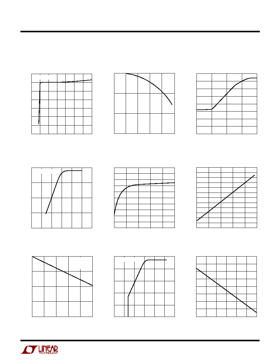
Efficiency vs Output Current
and Mode (Figure 13)
OUTPUT CURRENT (A)
0.001
0
EFFICIENCY (%)
10
30
40
50
100
70
0.01
0.1
1
1628 G01
20
80
90
60
10
FORCED
CONTINUOUS
MODE
CONSTANT
FREQUENCY
(BURST DISABLE)
Burst Mode
OPERATION
V
IN
= 15V
V
OUT
= 5V
OUTPUT CURRENT (A)
0.001
EFFICIENCY (%)
70
80
10
1628 G02
60
50
0.01
0.1
1
100
90
V
IN
= 10V
V
IN
= 15V
V
IN
= 7V
V
IN
= 20V
V
IN
= 15V
V
OUT
= 5V
INPUT VOLTAGE (V)
5
EFFICIENCY (%)
70
80
1628 G03
60
50
15
25
35
100
V
OUT
= 5V
I
OUT
= 3A
90
Efficiency vs Output Current
(Figure 13)
Efficiency vs Input Voltage
(Figure 13)
INTV
CC
and EXTV
CC
Switch
Voltage vs Temperature
Supply Current vs Input Voltage
and Mode (Figure 13)
INPUT VOLTAGE (V)
0
5
0
SUPPLY CURRENT (
µ
A)
400
1000
10
20
25
1628 G04
200
800
600
15
30
35
BOTH
CONTROLLERS ON
STANDBY
SHUTDOWN
EXTV
CC
Voltage Drop
CURRENT (mA)
0
EXTV
CC
VOLTAGE DROP (mV)
150
200
250
40
1628 G05
100
50
0
10
20
30
50
TEMPERATURE (
∞
C)
≠ 50
INTV
CC
AND EXTV
CC
SWITCH VOLTAGE (V)
4.95
5.00
5.05
25
75
1628 G06
4.90
4.85
≠ 25
0
50
100
125
4.80
4.70
4.75
INTV
CC
VOLTAGE
EXTV
CC
SWITCHOVER THRESHOLD
ELECTRICAL CHARACTERISTICS
TYPICAL PERFOR A CE CHARACTERISTICS
U
W
5
LTC1628/LTC1628-PG
Internal 5V LDO Line Reg
Maximum Current Sense Threshold
vs Duty Factor
Maximum Current Sense Threshold
vs Percent of Nominal Output
Voltage (Foldback)
INPUT VOLTAGE (V)
0
4.8
4.9
5.1
15
25
1628 G07
4.7
4.6
5
10
20
30
35
4.5
4.4
5.0
INTV
CC
VOLTAGE (V)
I
LOAD
= 1mA
DUTY FACTOR (%)
0
0
V
SENSE
(mV)
25
50
75
20
40
60
80
1628 G08
100
PERCENT ON NOMINAL OUTPUT VOLTAGE (%)
0
V
SENSE
(mV)
40
50
60
100
1628 G09
30
20
0
25
50
75
10
80
70
Maximum Current Sense Threshold
vs V
RUN/SS
(Soft-Start)
V
RUN/SS
(V)
0
0
V
SENSE
(mV)
20
40
60
80
1
2
3
4
1628 G10
5
6
V
SENSE(CM)
= 1.6V
Maximum Current Sense Threshold
vs Sense Common Mode Voltage
COMMON MODE VOLTAGE (V)
0
V
SENSE
(mV)
72
76
80
4
1628 G11
68
64
60
1
2
3
5
Current Sense Threshold
vs I
TH
Voltage
V
ITH
(V)
0
V
SENSE
(mV)
30
50
70
90
2
1628 G12
10
≠10
20
40
60
80
0
≠20
≠30
0.5
1
1.5
2.5
Load Regulation
LOAD CURRENT (A)
0
NORMALIZED V
OUT
(%)
≠0.2
≠0.1
4
1628 G13
≠0.3
≠0.4
1
2
3
5
0.0
FCB = 0V
V
IN
= 15V
FIGURE 1
V
ITH
vs V
RUN/SS
V
RUN/SS
(V)
0
0
V
ITH
(V)
0.5
1.0
1.5
2.0
2.5
1
2
3
4
1628 G14
5
6
V
OSENSE
= 0.7V
SENSE Pins Total Source Current
V
SENSE
COMMON MODE VOLTAGE (V)
0
I
SENSE
(
µ
A)
0
1628 G15
≠50
≠100
2
4
50
100
6
TYPICAL PERFOR A CE CHARACTERISTICS
U
W