1
LTC1685
FEATURES
APPLICATIO S
U
TYPICAL APPLICATIO
N
U
DESCRIPTIO
U
52Mbps, Precision Delay,
RS485 Fail-Safe Transceiver
s
Precision Propagation Delay Over Temperature:
Receiver/Driver: 18.5ns
±
3.5ns
s
High Data Rate:
52Mbps
s
Low t
PLH
/t
PHL
Skew:
Receiver/Driver: 500ps Typ
s
≠7V to 12V RS485 Input Common Mode Range
s
Guaranteed Fail-Safe Receiver Operation Over the
Entire Common Mode Range
s
High Receiver Input Resistance:
22k, Even When
Unpowered
s
Short-Circuit Protected
s
Thermal Shutdown Protected
s
Driver Maintains High Impedance in Three-State or
with Power Off
s
Single 5V Supply
s
Pin Compatible with LTC485
s
45dB CMRR at 26MHz
The LTC
Æ
1685 is a high speed, precision delay RS485
transceiver that can operate at data rates as high as 52Mbps.
The device also meets the requirements of RS422.
A unique architecture provides very stable propagation
delays and low skew over a wide common mode and
ambient temperature range.
The driver and receiver feature three-state outputs, with
disabled driver outputs maintaining high impedance over
the entire common mode range. A short circuit feature
detects shorted outputs and substantially reduces driver
output current. A similar feature also protects the receiver
output from short circuits. Thermal shutdown circuitry
protects from excessive power dissipation.
The receiver has a fail-safe feature that guarantees a high
output state when the inputs are shorted or are left floating.
The LTC1685 RS485 transceiver guarantees receiver fail-
safe operation over the
entire common mode range (≠ 7V
to 12V). Input resistance will remain
22k when the device
is unpowered or disabled.
The LTC1685 operates from a single 5V supply and draws
only 7mA of supply current.
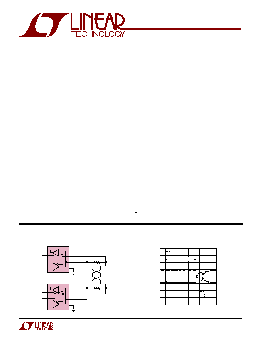
10Mbps Data Pulse
400ft Category 5 UTP
1685 TA02
DRIVER INPUT
RECEIVER
INPUT
RECEIVER
OUTPUT
100ns/DIV
1V/DIV
2V/DIV
5V/DIV
CABLE DELAY
, LTC and LT are registered trademarks of Linear Technology Corporation.
s
High Speed RS485/RS422 Transceivers
s
Level Translator
s
Backplane Transceiver
s
STS-1/OC-1 Data Transceiver
s
Fast-20, Fast-40 SCSI Transceivers
V
CC1
GND1
R
RO1
RE1
DE1
DI1
D
Rt
Rt
1685 TA01
V
CC2
GND2
R
RO2
RE2
DE2
DI2
D
2
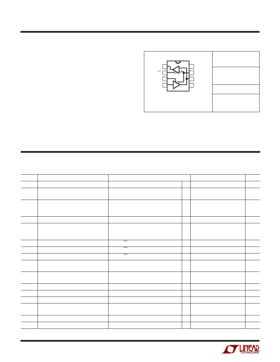
LTC1685
W
U
U
PACKAGE/ORDER I FOR ATIO
A
U
G
W
A
W
U
W
A
R
BSOLUTE
XI
TI
S
(Note 1)
Supply Voltage (V
DD
) .............................................. 10V
Control Input Currents .................... ≠ 100mA to 100mA
Control Input Voltages .................. ≠ 0.5V to V
DD
+ 0.5V
Driver Input Voltages .................... ≠ 0.5V to V
DD
+ 0.5V
Driver Output Voltages .................................. +12V/≠ 7V
Receiver Input Voltages ................................. +12V/≠ 7V
Receiver Output Voltages ............. ≠ 0.5V to V
DD
+ 0.5V
Receiver Input Differential ...................................... 10V
Short-Circuit Duration (Driver V
OUT
: ≠ 7V to 10V,
Receiver V
OUT
: 0V to V
DD
) ............................... Indefinite
Operating Temperature Range
LTC1685C ............................................... 0
∞
C to 70
∞
C
LTC1685I ............................................. ≠40
∞
C to 85
∞
C
Storage Temperature Range ................ ≠ 65
∞
C to 150
∞
C
Lead Temperature (Soldering, 10 sec)................. 300
∞
C
ORDER PART
NUMBER
1
2
3
4
8
7
6
5
TOP VIEW
V
DD
B
A
GND
S8 PACKAGE
8-LEAD PLASTIC SO
RO
RE
DE
DI
R
D
T
JMAX
= 125
∞
C,
JA
= 150
∞
C/ W
Consult factory for Military grade parts.
S8 PART MARKING
DC ELECTRICAL CHARACTERISTICS
SYMBOL
PARAMETER
CONDITIONS
MIN
TYP
MAX
UNITS
V
OD1
Differential Driver Output (Unloaded)
I
OUT
= 0
q
V
DD
V
V
OD2
Differential Driver Output (With Load)
R = 50
(RS422)
2
V
R = 27
(RS485), Figure 1
q
1.5
V
DD
V
V
OD
Change in Magnitude of Driver Differential
R = 27
or 50
, Figure 1
q
0.2
V
Output Voltage for Complementary
Output States
V
OC
Driver Common Mode Output Voltage
R = 27
or 50
, V
DD
= 5V, Figure 1
q
2
3
V
V
OC
Change in Magnitude of Driver Common
R = 27
or 50
, Figure 1
q
0.2
V
Mode Output Voltage for Complementary
Output States
V
IH
Input High Voltage
DE, DI, RE
q
2
V
V
IL
Input Low Voltage
DE, DI, RE
q
0.8
V
I
IN1
Input Current
DE, DI, RE
q
≠ 1
1
µ
A
I
IN2
Input Current (A, B)
V
A
, V
B
= 12V, DE = 0, V
DD
= 0V or 5.25V
q
500
µ
A
V
A
, V
B
= ≠ 7V, DE = 0, V
DD
= 0V or 5.25V
q
≠ 500
µ
A
V
TH
Differential Input Threshold Voltage
≠ 7V
V
CM
12V
q
≠ 0.3
0.3
V
for Receiver
V
TH
Receiver Input Hysteresis
V
CM
= 0V
25
mV
V
OH
Receiver Output High Voltage
I
OUT
= ≠ 4mA, V
ID
= 300mV
q
3.5
4.8
V
V
OL
Receiver Output Low Voltage
I
OUT
= 4mA, V
ID
= ≠ 300mV
q
0.4
V
I
OZR
Three-State (High Impedance) Output
0.4V
V
OUT
2.4V
q
≠ 1
1
µ
A
Current at Receiver
I
DD
Supply Current
No Load, Pins 2, 3, 4 = 0V or V
DD
q
7
12
mA
I
OSD1
Driver Short-Circuit Current, V
OUT
= HIGH
V
OUT
= ≠ 7V or 10V (Note 5)
q
20
mA
LTC1685CS8
LTC1685IS8
1685
1685I
The
q
denotes the specifications which apply over the full operating
temperature range, otherwise specifications are at T
A
= 25
∞
C. V
DD
= 5V
±
5%, unless otherwise noted. (Notes 2, 3)
3
LTC1685
SYMBOL
PARAMETER
CONDITIONS
MIN
TYP
MAX
UNITS
t
PLH
, t
PHL
Driver Input-to-Output
R
DIFF
= 54
, C
L1
= C
L2
= 100pF, Figures 3, 5,
Propagation Delay
LTC1685C
q
15
18.5
22
ns
LTC1685I
q
13
18.5
25
ns
t
SKEW
Driver Output A-to-Output
R
DIFF
= 54
, C
L1
= C
L2
= 100pF,
500
ps
B Skew
Figures 3, 5
t
r
, t
f
Driver Rise/Fall Time
R
DIFF
= 54
, C
L1
= C
L2
= 100pF,
3.5
ns
Figures 3, 5
t
ZH
Driver Enable to Output High
C
L
= 100pF, S2 Closed, Figures 4, 6
q
25
50
ns
t
ZL
Driver Enable to Output Low
C
L
= 100pF, S1 Closed, Figures 4, 6
q
25
50
ns
t
LZ
Driver Disable from Low
C
L
= 15pF, S1 Closed, Figures 4, 6
q
25
50
ns
t
HZ
Driver Disable from High
C
L
= 15pF, S2 Closed, Figures 4, 6
q
25
50
ns
t
PLH
, t
PHL
Receiver Input-to-Output
C
L
= 15pF, Figures 3, 7
Propagation Delay
LTC1685C
q
15
18.5
22
ns
LTC1685I
q
13
18.5
25
ns
t
SQD
Receiver Skew
t
PLH
≠ t
PHL
C
L
= 15pF, Figures 3, 7
500
ps
t
ZL
Receiver Enable to Output Low
C
L
= 15pF, S1 Closed, Figures 2, 8
q
25
50
ns
t
ZH
Receiver Enable to Output High
C
L
= 15pF, S2 Closed, Figures 2, 8
q
25
50
ns
t
LZ
Receiver Disable from Low
C
L
= 15pF, S1 Closed, Figures 2, 8
q
25
50
ns
t
HZ
Receiver Disable from High
C
L
= 15pF, S2 Closed, Figures 2, 8
q
25
50
ns
Maximum Receiver Input
(Note 4)
q
2000
ns
Rise/Fall Times
t
PKG-PKG
Package-to-Package Skew
Same Temperature (Note 4)
1.5
ns
Minimum Input Pulse Width
V
DD
= 5V
±
5% (Note 4)
LTC1685C
q
17
19.2
ns
LTC1685I
q
20
25
ns
Maximum Data Rate
V
DD
= 5V
±
5% (Note 4)
LTC1685C
q
52
60
Mbps
LTC1685I
q
40
50
Mbps
Maximum Input Frequency
V
DD
= 5V
±
5% (Note 4)
LTC1685C
q
26
30
MHz
LTC1685I
q
20
25
MHz
SYMBOL
PARAMETER
CONDITIONS
MIN
TYP
MAX
UNITS
I
OSD2
Driver Short-Circuit Current, V
OUT
= LOW
V
OUT
= ≠ 7V or 10V (Note 5)
q
20
mA
I
OSR
Receiver Short-Circuit Current
V
OUT
= 0V or V
DD
(Note 5)
q
20
mA
R
IN
Input Resistance
≠ 7V
V
CM
12V
q
22
k
C
IN
Input Capacitance
A, B Inputs, D, DE, RE
3
pF
Open-Circuit Input Voltage, Figure 5
V
DD
= 5V (Note 4)
q
3.2
3.3
3.4
V
Fail-Safe Time Time to Detect Fail-Safe Condition
2
µ
s
CMRR
Receiver Input Common Mode Rejection Ratio
V
CM
= 2.6V, f = 26MHz
45
dB
C
LOAD
Receiver and Driver Output Load Capacitance
(Note 4)
q
500
pF
DC ELECTRICAL CHARACTERISTICS
SWITCHI
N
G CHARACTERISTICS
U
The
q
denotes the specifications which apply over the full operating
temperature range, otherwise specifications are at T
A
= 25
∞
C. V
DD
= 5V
±
5%, unless otherwise noted. (Notes 2, 3)
The
q
denotes the specifications which apply over the full operating
temperature range, otherwise specifications are at T
A
= 25
∞
C. V
DD
= 5V, unless otherwise noted. (Notes 2, 3)
4
LTC1685
TYPICAL PERFOR
M
A
N
CE CHARACTERISTICS
U
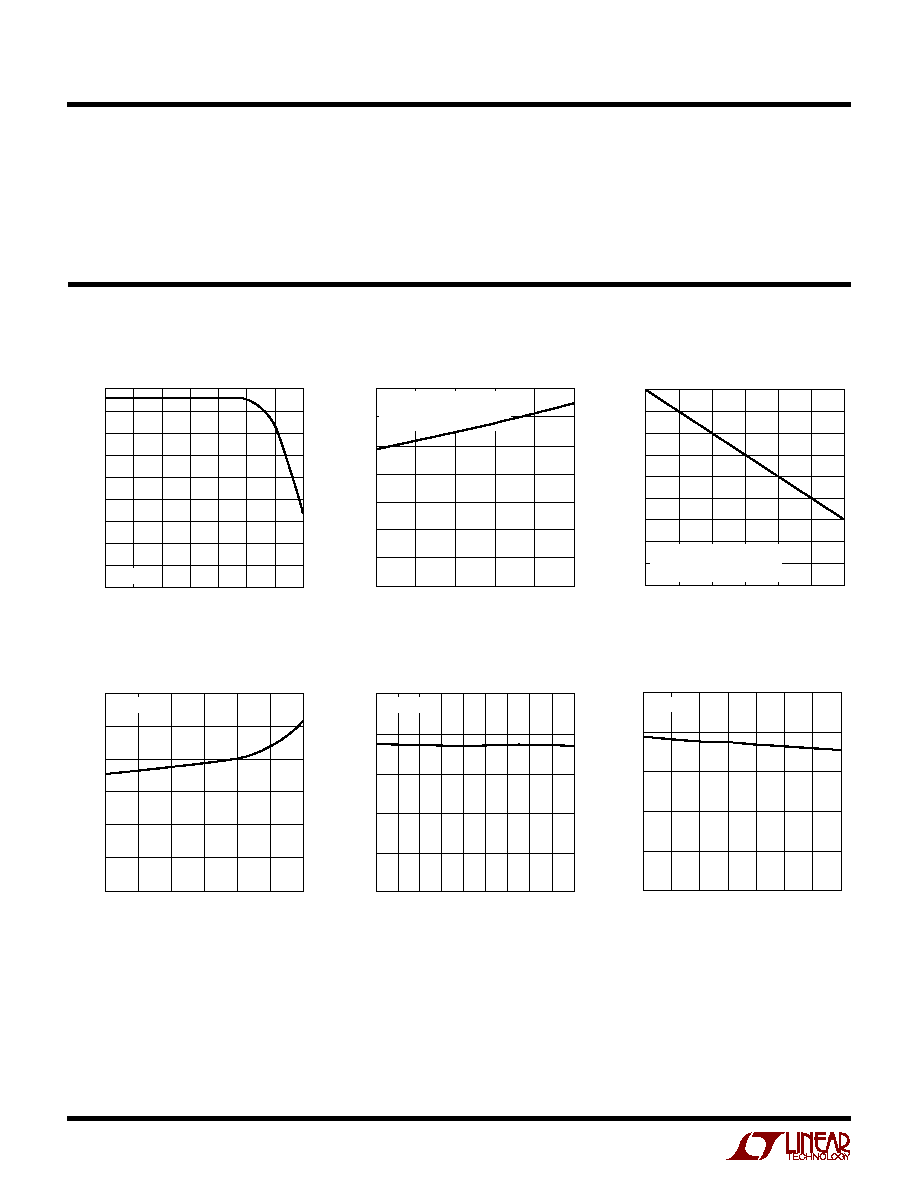
W
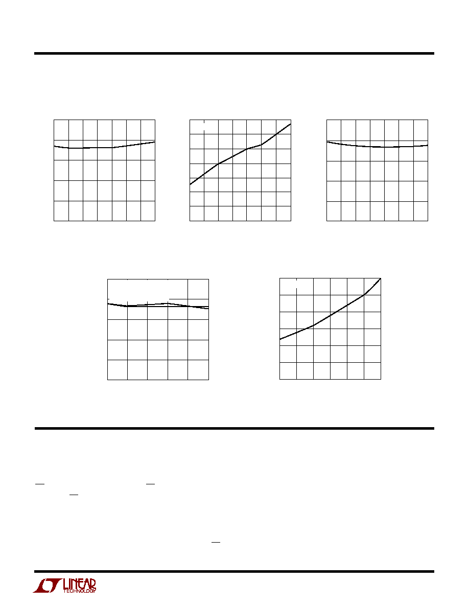
FREQUENCY (Hz)
10
42.0
COMMON MODE REJECTION RATIO (dB)
42.5
43.5
44.0
44.5
46.5
1685 G01
43.0
1k
100k
1M
45.0
45.5
46.0
T
A
= 25
∞
C
Receiver Input CMRR
TEMPERATURE (
∞
C)
≠50
≠ 25
SUPPLY CURRENT (mA)
53
54
55
50
100
1685 G03
52
51
50
0
25
75
56
57
59
58
BOTH DRIVER AND RECEIVER
ENABLED AND LOADED
25Mbps DATA RATE
DATA RATE (Mbps)
1
50
60
70
40
30
1685 G02
40
30
10
20
50
20
10
0
SUPPLY CURRENT (mA)
BOTH DRIVER AND RECEIVER
ENABLED AND LOADED
T
A
= 25
∞
C
Supply Current vs Data Rate
Supply Current vs Temperature
Receiver Propagation Delay
vs Load Capacitance
Receiver Propagation Delay
vs Common Mode
LOAD CAPACITANCE (pF)
5
0
PROPAGATION DELAY (ns)
5
10
15
20
30
15
25
35
55
1685 G04
105
205
25
T
A
= 25
∞
C
RECEIVER COMMON MODE (V)
≠ 7
0
PROPAGATION DELAY (ns)
5
15
20
25
≠ 2
2
4
12
1685 G05
10
≠ 4
0
6
8
10
T
A
= 25
∞
C
Receiver Propagation Delay
vs Input Overdrive
RECEIVER INPUT OVERDRIVE (V)
0.3
0.5
0
RECEIVER PROPAGATION DELAY (ns)
10
25
0.7
1.25
1.5
1685 G06
5
20
15
1.0
2.0
2.5
T
A
= 25
∞
C
Note 1: Absolute Maximum Ratings are those values beyond which the life
of a device may be impaired.
Note 2: All currents into the device pins are positive; all currents out of the
device pins are negative.
Note 3: All typicals are given for V
DD
= 5V, T
A
= 25
∞
C.
Note 4: Guaranteed by design, but not tested.
Note 5: Short-circuit current does not represent output drive capability.
When the output detects a short-circuit condition, output drive current is
significantly reduced (from hundreds of mA to 20mA max) until the short
is removed.
SWITCHI
N
G CHARACTERISTICS
U
5
LTC1685
TYPICAL PERFOR
M
A
N
CE CHARACTERISTICS
U
W
DI (Pin 4): Driver Input. Controls the states of the A and
B outputs only if DE = High. If DE = Low, DI will have no
effect on A and B pins. Do not float.
GND (Pin 5): Ground.
A (Pin 6): Noninverting Receiver Input/Driver Output.
B (Pin 7): Inverting Receiver Input/Driver Output.
V
DD
(Pin 8): Positive Supply, 5V to
±
5%. Bypass with
0.1
µ
F ceramic capacitor.
PI
N
FU
N
CTIO
N
S
U
U
U
RO (Pin 1): Receiver Output. If A
B by 300mV, then RO
will be high. If A
B by 300mV, then RO will be low.
RE (Pin 2): Receiver Enable. RE = Low enables the
receiver. RE = High forces receiver output into high
impedance state. Do not float.
DE (Pin 3): Driver Enable. DE = High enables the driver.
DE = Low will force the driver output into a high impedance
state and the device will function as a line receiver if RE is
also low. Do not float.
Driver Propagation Delay
vs Temperature
Driver Propagation Delay
vs Driver Input Voltage
DRIVER INPUT VOLTAGE (V)
2.5
PROPAGATION DELAY (ns)
15
20
25
4.5
1685 G08
10
5
0
3.0
3.5
4.0
5.0
t
LH
V
DD
= 5V
INPUT THRESHOLD = 1.5V
T
A
= 25
∞
C
t
HL
Driver Propagation Delay
vs Capacitive Load
LOAD CAPACITANCE (pF)
5
16.0
PROPAGATION DELAY (ns)
16.5
17.0
17.5
18.0
19.0
15
25
50
75
1685 G11
100
150
18.5
T
A
= 25
∞
C
Receiver Maximum Data Rate
vs Input Overdrive
Receiver Propagation Delay
vs Temperature
TEMPERATURE (
∞
C)
≠50
≠25
0
PROPAGATION DELAY (ns)
10
25
0
50
75
1680 G09
5
20
15
25
100
125
RECEIVER INPUT DIFFERENTIAL (V)
0.3
40
50
70
0.6
1.0
1685 G10
30
20
0.4
0.5
0.7
1.5
2.5
10
0
60
DATA RATE (Mbps)
T
A
= 25
∞
C
TEMPERATURE (
∞
C)
≠ 20
≠ 40
0
PROPAGATION DELAY (ns)
5
10
15
20
25
0
20
40
60
1685 G07
80
100
6
LTC1685
FU CTIO TABLES
U
U
Transmitting
INPUTS
LINE
OUTPUTS
RE
DE
DI
CONDITION
B
A
X
1
1
No Fault
0
1
X
1
0
No Fault
1
0
X
0
X
X
Hi-Z
Hi-Z
X
1
X
Fault
Receiving
INPUTS
OUTPUT
RE
DE
A ≠ B
RO
0
0
300mV
1
0
0
≠ 300mV
0
0
0
Inputs Open
1
0
0
Inputs Shorted Together
1
A = B = ≠ 7V to 12V
1
X
X
Hi-Z
±
10mA Current Source
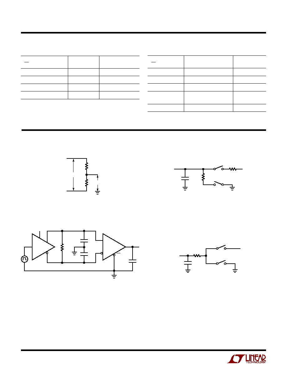
TEST CIRCUITS
V
OD
A
B
R
R
V
OC
1685 F01
Figure 1. Driver DC Test Load
RECEIVER
OUTPUT
C
L
15pF
1k
S1
S2
TEST POINT
V
DD
1k
1685 F02
Figure 2. Driver DC Test Load
OUTPUT
UNDER TEST
C
L
S1
S2
V
DD
500
1685 F04
Figure 3. Driver/Receiver Timing Test Circuit
Figure 4. Driver Timing Test Load #2
3V
DE
A
B
DI
R
DIFF
C
L1
C
L2
RO
15pF
A
B
RE
1685 F03
7
LTC1685
SWITCHI G TI E WAVEFOR S
U
W
W
Figure 5. Driver Propagation Delays
DI
3V
1.5V
t
PLH
t
r
t
SKEW
1/2 V
O
90%
10%
0V
B
A
V
O
≠V
O
0V
90%
1.5V
t
PHL
t
SKEW
1/2 V
O
f = 1MHz, t
r
3ns, t
f
3ns
10%
t
f
V
DIFF
= V(A) ≠ V(B)
1586 F05
V
O
Figure 8. Receiver Enable and Disable Times
Figure 7. Receiver Propagation Delays
2.5V
t
PHL
f = 1MHz, t
r
3ns, t
f
3ns
RO
≠V
OD2
A ≠ B
0V
2.5V
t
PLH
OUTPUT
INPUT
V
OD2
V
OL
V
OH
1686 F07
1.5V
t
ZL
2.5V
2.5V
t
ZH
1.5V
t
LZ
0.5V
0.5V
t
HZ
f = 1MHz, t
r
3ns, t
f
3ns
OUTPUT NORMALLY LOW
OUTPUT NORMALLY HIGH
3V
0V
DE
5V
V
OL
V
OH
0V
A, B
A, B
1686 F06
Figure 6. Driver Enable and Disable Times
1.5V
t
ZL
2.5V
2.5V
t
ZH
1.5V
t
LZ
0.5V
0.5V
t
HZ
f = 1MHz, t
r
3ns, t
f
3ns
OUTPUT NORMALLY LOW
OUTPUT NORMALLY HIGH
3V
0V
RE
5V
0V
RO
RO
1685 F08

8
LTC1685
A
B
1685 F09
22k
3.3V
22k
3.3V
DE = 0, RE = 0 OR 1
V
DD
= 5V
V
DD
= 0V
A
B
22k
22k
APPLICATIO
N
S I
N
FOR
M
ATIO
N
W
U
U
U
Theory of Operation
Unlike typical CMOS transceivers whose propagation
delay can vary by as much as 500% from package to
package and show significant temperature drift, the
LTC1685 employs a novel architecture that produces a
tightly controlled and temperature compensated propaga-
tion delay. The differential timing skew is also minimized
between rising and falling output edges of the receiver
output and the complementary driver outputs.
The precision timing features of the LTC1685 reduce
overall system timing constraints by providing a narrow
±
3.5ns window during which valid data appears at the
receiver/driver output. The driver and receiver pair will
have propagation delays that typically match to within 1ns.
In clocked data systems, the low skew minimizes duty
cycle distortion of the clock signal. The LTC1685 can be
used at data rates of 52Mbps with less than 5% duty cycle
distortion (depending on cable length). When a clock
signal is used to retime parallel data, the maximum recom-
mended data transmission rate is 26Mbps to avoid timing
errors due to clock distortion.
Fail-Safe Features
The LTC1685 has a fail-safe feature that guarantees the
receiver output to be in a logic HIGH state when the inputs
are either shorted or left open (note that when inputs are
left open, large external leakage currents might override
the fail-safe circuitry). In order to maintain good high
frequency performance, it was necessary to slow down
the transient response of the fail-safe feature. When a line
fault is detected, the output will go HIGH typically in 2
µ
s.
Note that the LTC1685 guarantees fail-safe performance
over the
entire (≠ 7V to 12V) common mode range!
When the inputs are accidentally shorted (by cutting
through a cable, for example), the short circuit fail-safe
feature will guarantee a high output logic level. Note also
that if the line driver is removed and the termination
resistors are left in place, the receiver will see this as a
"short" and output a logic HIGH. Both of these fail-safe
features will keep the receiver from outputting false data
pulses under line fault conditions.
Thermal shutdown and short-circuit protection prevent
latchup damage to the LTC1685 during fault conditions.
Figure 9. Input Thevenin Equivalent
EQUIVALE
N
T I
N
PUT
N
ETWORKS
U
U
U
9
LTC1685
Output Short-Circuit Protection
The LTC1685 employs voltage sensing short-circuit pro-
tection at the output terminals of both the driver and
receiver. For a given input polarity, this circuitry deter-
mines what the correct output level should be. If the output
level is different from the expected, it shuts off the big
output devices. For example, if the driver input is >2V, it
expects the "A" output to be >3.25V and the "B" output to
be <1.75V. If the "A" output is subsequently shorted to a
voltage below V
DD
/2, this circuitry shuts off the big output
devices and turns on a smaller device in its place (the
converse applies for the "B" output). The outputs then
appear as
±
10mA current sources. Note that under normal
operation, the output drivers can sink/source >50mA. A
time-out period of about 50ns is used in order to maintain
normal high frequency operation, even under heavy ca-
pacitive loads.
If the cable is shorted at a large distance from the device
outputs, it is possible for the short to go unnoticed at the
driver outputs due to parasitic cable resistance. Addition-
ally, when the cable is shorted, it no longer appears as an
ideal transmission line, and the parasitic Ls and Cs might
give rise to ringing and even oscillation. All these conditions
disappear once the device comes out of short-circuit mode.
For cables with the typical RS485 termination (no DC bias
on the cable, such as Figure 10), the LTC1685 will auto-
matically come out of short-circuit mode once the physical
short has been removed. With cable terminations with a
DC bias (such as Fast-20 and Fast-40 differential SCSI
APPLICATIO
N
S I
N
FOR
M
ATIO
N
W
U
U
U
terminators, see Figure 15), the LTC1685 will
not come
out of short-circuit mode automatically upon release of the
physical short. In order to resume normal operation, the
DE pin has to be pulsed low for at least 200ns.
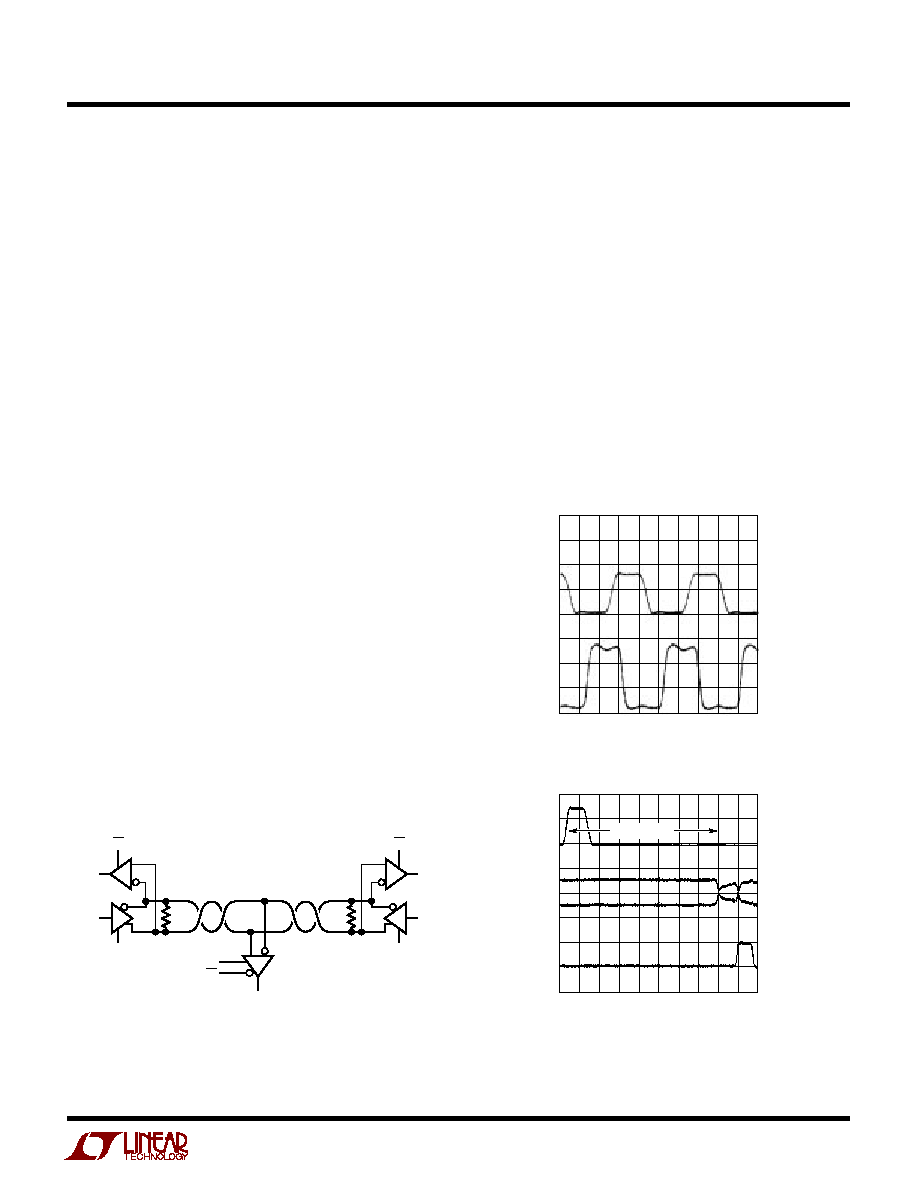
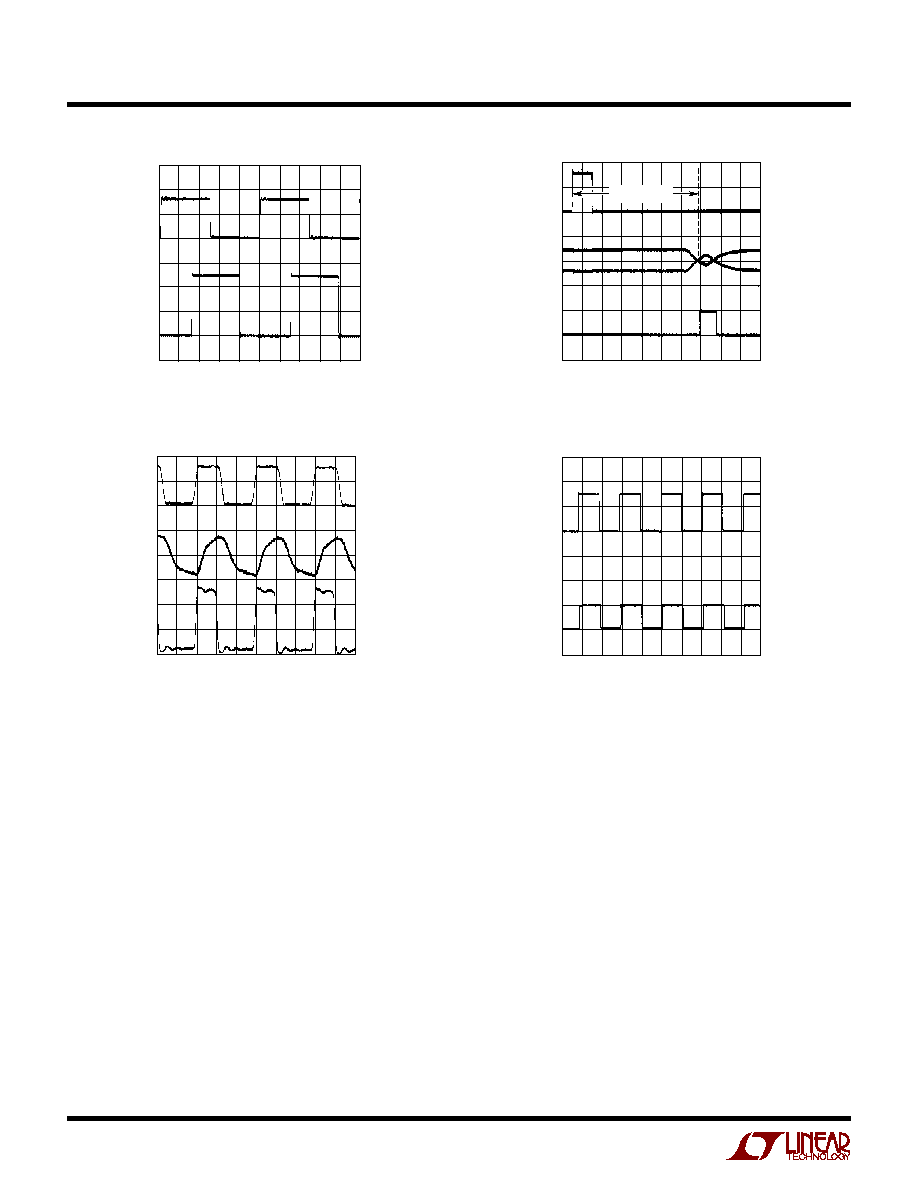
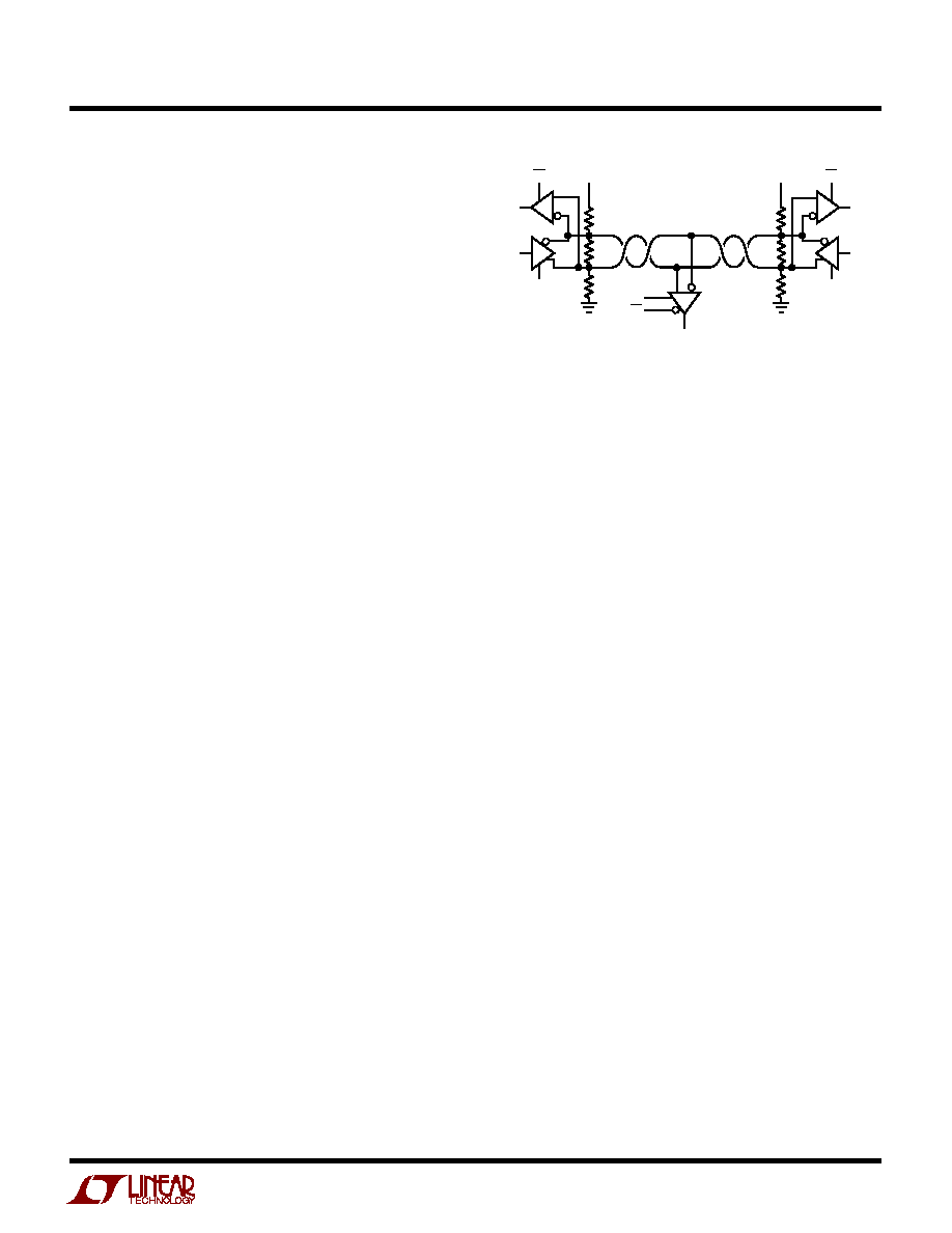
High Speed Twisted Pair Transmission
Data rates up to 52Mbps can be transmitted over 100ft of
category 5 twisted pair. Figure 10 shows the LTC1685
receiving differential data from another LTC1685 trans-
ceiver. Figure 11a shows a 26MHz (52Mbps) square wave
propagated over 100ft of category 5 UTP. Figure 11b
shows a more stringent case of propagating a single 20ns
pulse over 100ft of category 5 UTP. Figure 12 shows a
4Mbps square wave over 1000ft of category 5 unshielded
twisted pair.
1685 F11
DRIVER
INPUT
RECEIVER
OUTPUT
10ns/DIV
2V/DIV
2V/DIV
Figure 11a. 100ft of Category 5 UTP: 50Mbps
1685 F11b
RECEIVER
INPUT
DRIVER
INPUT
RECEIVER
OUTPUT
20ns/DIV
2V/DIV
5V/DIV
2V/DIV
CABLE DELAY
Figure 11b. 100ft of Category 5 UTP: 20ns Pulse
Figure 10
100
A 1
4
EN
RO
1685 F10b
1/4 LTC1518
LTC1685
LTC1685
12
3
2 B
7
6
3
2
DE
DI
RO
RE
4
1
100
7
6
3
2
DE
DI
RO
RE
4
1
EN
10
LTC1685
APPLICATIO
N
S I
N
FOR
M
ATIO
N
W
U
U
U
Very inexpensive unshielded telephone grade twisted pair
is shown in Figure 13. In spite of the noticeable loss at the
receiver input, the LTC1685 can still transfer 30Mbps at
100ft of telephone grade UTP. Note that under all these
conditions, the LTC1685 can pass through a single data
pulse equal to the inverse of the data rate (e.g., 20ns for
50Mbps data rate).
Even at distances of 4000ft, 1Mbps data rates are possible
using the LTC1685 and category 5 UTP. Figure 14a shows
a 1
µ
s pulse propagated down 4000ft of category 5 UTP.
Notice both the DC and the AC losses at the receiver input.
The DC attenuation is due to the parasitic resistance of the
cable. Figure 14b shows a 1Mbps square wave over
4000ft. To transmit at this speed but using longer cable
lengths, see the LTC1686/LTC1687 high speed RS485
full-duplex transceivers.
Figure 13. 100ft of Telephone Grade UTP: 30Mbps
Figure 12. 1000ft of Category 5 UTP: 4Mbps
1685 F13
DRIVER INPUT
DIFFERENTIAL
RECEIVER
INPUT
RECEIVER
OUTPUT
20ns/DIV
2V/DIV
2V/DIV
2V/DIV
1685 F12
DRIVER
INPUT
RECEIVER
OUTPUT
100ns/DIV
2V/DIV
2V/DIV
Figure 14b. 4000ft of Category 5 UTP: 1Mbps Square Wave
Figure 14a. 4000ft of Category 5 UTP: 1
µ
s Pulse
High Speed Backplane Transmission
The LTC1685 can also be used in backplane point-to-point
transceiver applications, where the user wants to assure
operation even when the common mode goes above or
below the rails. It is advisable to terminate the PC traces
when approaching maximum speeds. Since the LTC1685
is not intended to drive parallel terminated cables with
characteristic impedances much less than that of twisted
pair, both ends of the PC trace must be
series terminated
with the characteristic impedance of the trace. For best
results, the signal should be routed differentially. The true
and complement outputs of the LTC1685 should be routed
on adjacent layers of the PC board. The two traces should
be routed very symmetrically, minimizing and equalizing
parasitics to nearby signal and power/ground layers. For
single-ended transmission, route the series terminated
1685 F14a
RECEIVER
INPUT
DRIVER
INPUT
RECEIVER
OUTPUT
1
µ
s/DIV
1V/DIV
5V/DIV
2V/DIV
CABLE DELAY
1685 F14b
DRIVER
INPUT
RECEIVER
OUTPUT
1
µ
s/DIV
5V/DIV
2V/DIV
11
LTC1685
APPLICATIO
N
S I
N
FOR
M
ATIO
N
W
U
U
U
single-ended trace over an adjacent ground plane. Then
set the (bypassed) negative input of the receiver to roughly
2.5V. Note that single-ended operation might not reach
maximum speeds.
High Speed Differential SCSI (Fast-20, Fast-40 HVD)
The LTC1685's high speed, tight propagation delay win-
dow and matched driver/receiver propagation delays make
it a natural choice as the external transceiver in high speed
differential SCSI applications. Note that the
±
3.5ns propa-
gation delay window covers the entire commercial tem-
perature range. If, for example, a group of 16 transceivers
is placed on the same board, their temperature difference
will be much smaller. Hence, the difference in their propa-
gation delays should be even better than the
±
3.5ns
specification (typically better than
±
2ns). The LTC1685 is
the most efficient and reliable implementation that meets
the Fast-20 and Fast-40 HVD driver and receiver skew
specifications.
Power-Up Requirements
The LTC1685 has unique short-circuit protection that
shuts off the big output devices (and keeps them off) when
a short is detected. When the LTC1685 is powered up with
the driver outputs enabled (Figure 15 shows a typical
connection), the part will power up in short-circuit mode.
After power-up, the user must hold the DE pin of the
LTC1685 low for at least 200ns in order to start normal
operation. Note also that turning the termination power
on/off might induce the LTC1685 to see a "short." Conse-
quently, the DE pin should be held low for 200ns after
cable termination power is turned on.
This requirement is solely due to the cable termination
(the 165
parallel resistance to both power and ground).
For applications whose connections to the cable are
made exclusively with RS485 devices, the cable can be
terminated
only across the two signal wires (as in Figure
10). With cable distances covering under 25 meters, the
common mode range of the LTC1685 should be more
than sufficient to account for any ground differences
between any two communicating devices. The fact that
transmission is differential should greatly improve noise
TERM POWER
150
330
330
330
330
A 1
4
EN
RO
1685 F15
1/4 LTC1518
LTC1685
LTC1685
12
3
2 B
7
6
3
2
DE
DI
RO
RE
TERM POWER
122
CABLE
4
1
150
7
6
3
2
DE
DI
RO
RE
4
1
EN
Figure 15. Fast-20, Fast-40 Differential SCSI Application
Information furnished by Linear Technology Corporation is believed to be accurate and reliable.
However, no responsibility is assumed for its use. Linear Technology Corporation makes no represen-
tation that the interconnection of its circuits as described herein will not infringe on existing patent rights.
margin. Furthermore, the good high frequency CMRR of
the receiver will serve to reject any common mode
interference.
DE, DI Inputs
It is not necessary that the driver input (DI) have 0V to 3V
signal levels. The DI input can be driven by CMOS levels
(0V to 5V) and still achieve 40Mbps operation. However,
duty cycle will be slightly compromised when driven by a
CMOS device. Care should be taken to minimize the
ringing on the DI input in order to achieve a driver
propagation delay within the
±
3.5ns window. This also
improves the package-to-package matching of propaga-
tion delays.
The DE pin should be held low for 200ns after the power-
up sequence has been completed. After fault conditions
such as an output short or thermal shutdown, the DE pin
should be held low for at least 200ns after the fault has
been removed. This is usually necessary only if the driver
outputs are connected to DC-biased cable terminations
(as in Figure 15).
Layout Considerations
A ground plane is recommended when using a high
frequency device like the LTC1685. A 0.1
µ
F ceramic by-
pass capacitor less than 1/4 inch away from the V
DD
pin is
recommended. Good bypassing is especially needed when
operating at maximum frequency or when package-to-
package matching is very important. The PC board traces
connected to the "A" and "B" outputs must be kept as
symmetrical and short as possible to obtain the same
12
LTC1685
Linear Technology Corporation
1630 McCarthy Blvd., Milpitas, CA 95035-7417
(408) 432-1900
q
FAX: (408) 434-0507
q
www.linear-tech.com
©
LINEAR TECHNOLOGY CORPORATION 1997
1685fa LT/LCG 0700 2K REV A ∑ PRINTED IN THE USA
PART NUMBER
DESCRIPTION
COMMENTS
LTC1485
High Speed RS485 Transceiver
10Mbps, Pin Compatible with LTC485
LTC1518/LTC1519
High Speed Quad RS485 Receivers
52Mbps, Pin Compatible with LTC488/LTC489
LTC1520
High Speed Quad Differential Receiver
52Mbps,
±
100mV Threshold, Rail-to-Rail Common Mode
LTC1686/LTC1687
High Speed RS485 Driver/Receiver
52Mbps, Pin Compatible with LTC490/LTC491
LTC1688/LTC1689
High Speed Quad RS485 Drivers
100Mbps, Pin Compatible with LTC486/LTC487
RELATED PARTS
SO8 0695
0.016 ≠ 0.050
0.406 ≠ 1.270
0.010 ≠ 0.020
(0.254 ≠ 0.508)
◊
45
∞
0
∞
≠ 8
∞
TYP
0.008 ≠ 0.010
(0.203 ≠ 0.254)
0.053 ≠ 0.069
(1.346 ≠ 1.752)
0.014 ≠ 0.019
(0.355 ≠ 0.483)
0.004 ≠ 0.010
(0.101 ≠ 0.254)
0.050
(1.270)
BSC
1
2
3
4
0.150 ≠ 0.157**
(3.810 ≠ 3.988)
8
7
6
5
0.189 ≠ 0.197*
(4.801 ≠ 5.004)
0.228 ≠ 0.244
(5.791 ≠ 6.197)
DIMENSION DOES NOT INCLUDE MOLD FLASH. MOLD FLASH
SHALL NOT EXCEED 0.006" (0.152mm) PER SIDE
DIMENSION DOES NOT INCLUDE INTERLEAD FLASH. INTERLEAD
FLASH SHALL NOT EXCEED 0.010" (0.254mm) PER SIDE
*
**
Dimensions in inches (millimeters) unless otherwise noted.
S8 Package
8-Lead Plastic Small Outline (Narrow 0.150)
(LTC DWG # 05-08-1610)
PACKAGE DESCRIPTIO
N
U
APPLICATIO
N
S I
N
FOR
M
ATIO
N
W
U
U
U
parasitic board capacitance. This maintains the good
matching characteristics of the low-to-high and high-to-
low transitions of the LTC1685. Note that output "A" to
output "B" capacitance should also be minimized. If routed
adjacent to each other on the same layer, they should be
separated by an amount at least as wide as the trace
widths. If output "A" and output "B" are routed on different
signal planes, they should not be routed directly on top of
each other. A trace width's lateral separation is also
recommended.
As mentioned before, care should also be taken when
routing the "DI" input. To achieve consistent board-to-
board propagation delay, the ringing on this signal should
be kept below a few hundred millivolts.