1
LTC1701
1MHz Step-Down
DC/DC Converter in SOT-23
December 1999
Final Electrical Specifications
Information furnished by Linear Technology Corporation is believed to be accurate and reliable.
However, no responsibility is assumed for its use. Linear Technology Corporation makes no represen-
tation that the interconnection of its circuits as described herein will not infringe on existing patent rights.
s
PDAs/Palmtop PCs
s
Digital Cameras
s
Cellular Phones
s
Portable Media Players
s
PC Cards
s
Handheld Equipment
, LTC and LT are registered trademarks of Linear Technology Corporation.
s
Tiny 5-Lead SOT-23 Package
s
Uses Tiny Capacitors and Inductor
s
High Frequency Operation: 1MHz
s
High Output Current: 500mA
s
Low R
DS(ON)
Internal Switch: 0.28
s
High Efficiency: Up to 94%
s
Current Mode Operation for Excellent Line
and Load Transient Response
s
Short-Circuit Protected
s
Low Quiescent Current: 135
µ
A
s
Low Dropout Operation: 100% Duty Cycle
s
Ultralow Shutdown Current: I
Q
< 1
µ
A
s
Peak Inductor Current Independent of Inductor Value
s
Output Voltages from 5V Down to 1.25V
APPLICATIO S
U
FEATURES
DESCRIPTIO
U
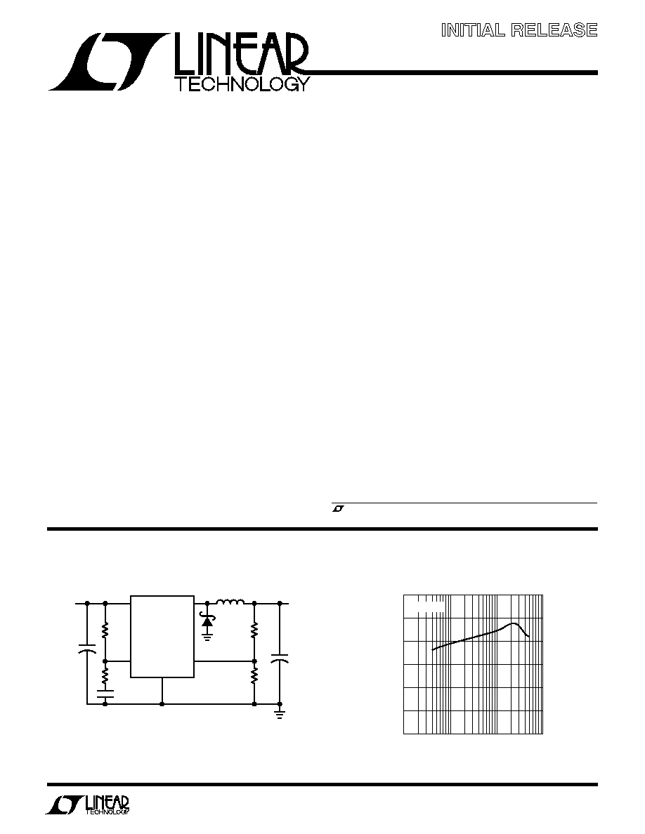
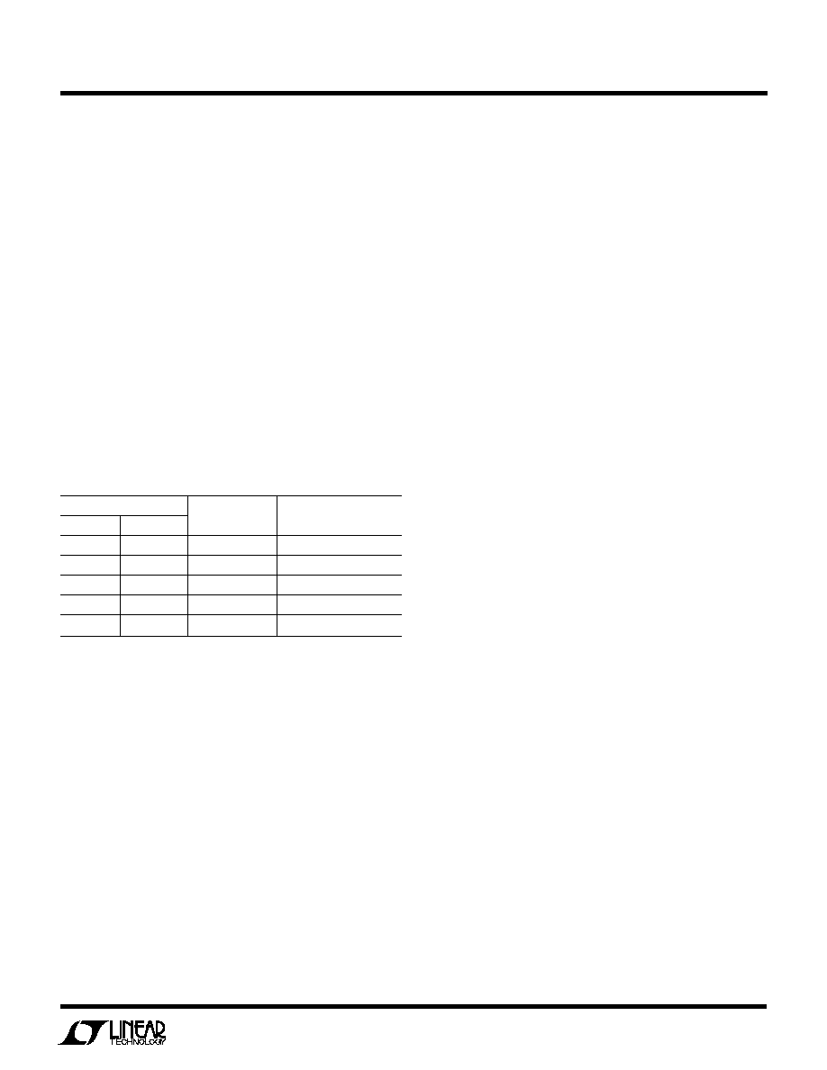
TYPICAL APPLICATIO
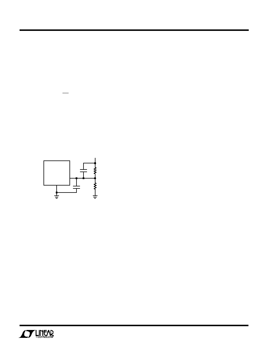
U
The LTC
Æ
1701 is the industry's first 5-lead SOT-23 step
down, current mode, DC/DC converter. Intended for small
to medium power applications, it operates from 2.5V to
5.5V input voltage range and switches at 1MHz, allowing
the use of tiny, low cost capacitors and inductors 2mm or
less in height. The output voltage is adjustable from 1.25V
to 5V. A built-in 0.28
switch allows up to 0.5A of output
current at high efficiency. OPTI-LOOP
TM
compensation
allows the transient response to be optimized over a wide
range of loads and output capacitors.
The LTC1701 incorporates automatic power saving Burst
Mode
TM
operation to reduce gate charge losses when the
load current drops below the level required for continuous
operation. With no load, the converter draws only 135
µ
A.
In shutdown, it draws less than 1
µ
A, making it ideal for
current sensitive applications.
In dropout, the internal P-channel MOSFET switch is
turned on continuously, thereby maximizing battery life.
Its small size and switching frequency enables the com-
plete DC/DC converter function to consume less than 0.3
square inches of PC board area.
V
IN
I
TH
/RUN
SW
V
FB
GND
LTC1701
D1
L1
4.7
µ
H
R4
1M
C1: TAIYO YUDEN JMK316BJ106ML
C2: SANYO POSCAP 6TPA47M
D1: MBRM120L
L1: SUMIDA CD43-4R7
R3
5.1k
C3
330pF
C1
10
µ
F
+
R2
121k
R1
121k
C2
47
µ
F
1701 F01
V
OUT
(2.5V/
500mA)
V
IN
2.5V TO
5.5V
+
Figure 1. Step-Down 2.5V/500mA Regulator
Efficiency Curve
Burst Mode and OPTI-LOOP are trademarks of Linear Technology Corporation.
LOAD CURRENT (mA)
1
10
100
1000
EFFICIENCY (%)
100
95
90
85
80
75
70
1701 F01a
V
IN
= 3.3V
2
LTC1701
ORDER PART
NUMBER
S5 PART
MARKING
T
JMAX
= 125
∞
C,
JA
= 110
∞
C/W
Consult factory for Industrial and Military grade parts.
LTKG
LTC1701ES5
ABSOLUTE AXI U
RATI GS
W
W
W
U
PACKAGE/ORDER I FOR ATIO
U
U
W
(Voltages Referred to GND Pin)
V
IN
Voltage (Pin 5).......................................≠ 0.3V to 6V
I
TH
/RUN Voltage (Pin 4) .............................. ≠ 0.3V to 3V
V
FB
Voltage (Pin 3) ...................................... ≠ 0.3V to 3V
Peak Switch Current (Pin 1) ................................... 1.3A
V
IN
≠ SW (Max Switch Voltage) ................8.5V to ≠ 0.3V
Operating Temperature Range (Note 2) .. ≠ 40
∞
C to 85
∞
C
Junction Temperature (Note 5) ............................. 125
∞
C
Storage Temperature Range ................. ≠ 65
∞
C to 150
∞
C
Lead Temperature (Soldering, 10 sec).................. 300
∞
C
(Note 1)
The
q
denotes the specifications which apply over the full operating
temperature range, otherwise specifications are at T
A
= 25
∞
C. V
IN
= 3.3V, R
ITH/RUN
= 1Meg (from V
IN
to I
TH
/RUN) unless otherwise
specified. (Note 2)
SYMBOL
PARAMETER
CONDITIONS
MIN
TYP
MAX
UNITS
V
IN
Operating Voltage Range
2.5
5.5
V
I
FB
Feedback Pin Input Current
(Note 3)
±
0.1
µ
A
V
FB
Feedback Voltage
(Note 3)
q
1.22
1.25
1.28
V
V
LINE REG
Reference Voltage Line Regulation
V
IN
= 2.5V to 5V (Note 3)
0.04
0.1
%/V
V
LOAD REG
Output Voltage Load Regulation
Measured in Servo Loop, V
ITH
= 1.5V, (Note 3)
0.01
0.70
%
Measured in Servo Loop, V
ITH
= 1.9V, (Note 3)
≠ 0.80
≠1.50
%
Input DC Supply Current (Note 4)
Active Mode
V
FB
= 0V
185
300
µ
A
Sleep Mode
V
FB
= 1.4V
135
200
µ
A
Shutdown
V
ITH/RUN
= 0V
0.25
1
µ
A
V
ITH/RUN
Run Threshold High
I
TH/RUN
Ramping Down
1.4
1.6
V
Run Threshold Low
I
TH/RUN
Ramping Up
0.3
0.6
V
I
ITH/RUN
Run Pullup Current
V
ITH/RUN
= 1V
50
100
300
µ
A
I
SW(PEAK)
Peak Switch Current Threshold
V
FB
= 0V
0.9
1.1
A
R
DS(ON)
Switch ON Resistance
V
IN
= 5V, V
FB
= 0V
0.28
V
IN
= 3.3V, V
FB
= 0V
0.30
V
IN
= 2.5V, V
FB
= 0V
0.35
I
SW(LKG)
Switch Leakage Current
V
IN
= 5V, V
ITH/RUN
= 0V, V
FB
= 0V
0.01
1
µ
A
t
OFF
Switch Off-Time
400
500
600
ns
ELECTRICAL CHARACTERISTICS
Note 1: Absolute Maximum Ratings are those values beyond which the life
of a device may be impaired.
Note 2: The LTC1701E is guaranteed to meet performance specifications
from 0
∞
C to 70
∞
C. Specifications over the ≠ 40
∞
C to 85
∞
C operating
temperature range are assured by design, characterization and correlation
with statistical process controls.
Note 3: The LTC1701 is tested in a feedback loop which servos V
FB
to the
midpoint for the error amplifier (V
ITH
= 1.7V unless otherwise specified).
Note 4: Dynamic supply current is higher due to the internal gate charge
being delivered at the switching frequency.
Note 5: T
J
is calculated from the ambient T
A
and power dissipation P
D
according to the following formula:
LTC1701ES5: T
J
= T
A
+ (P
D
∑110
∞
C/W)
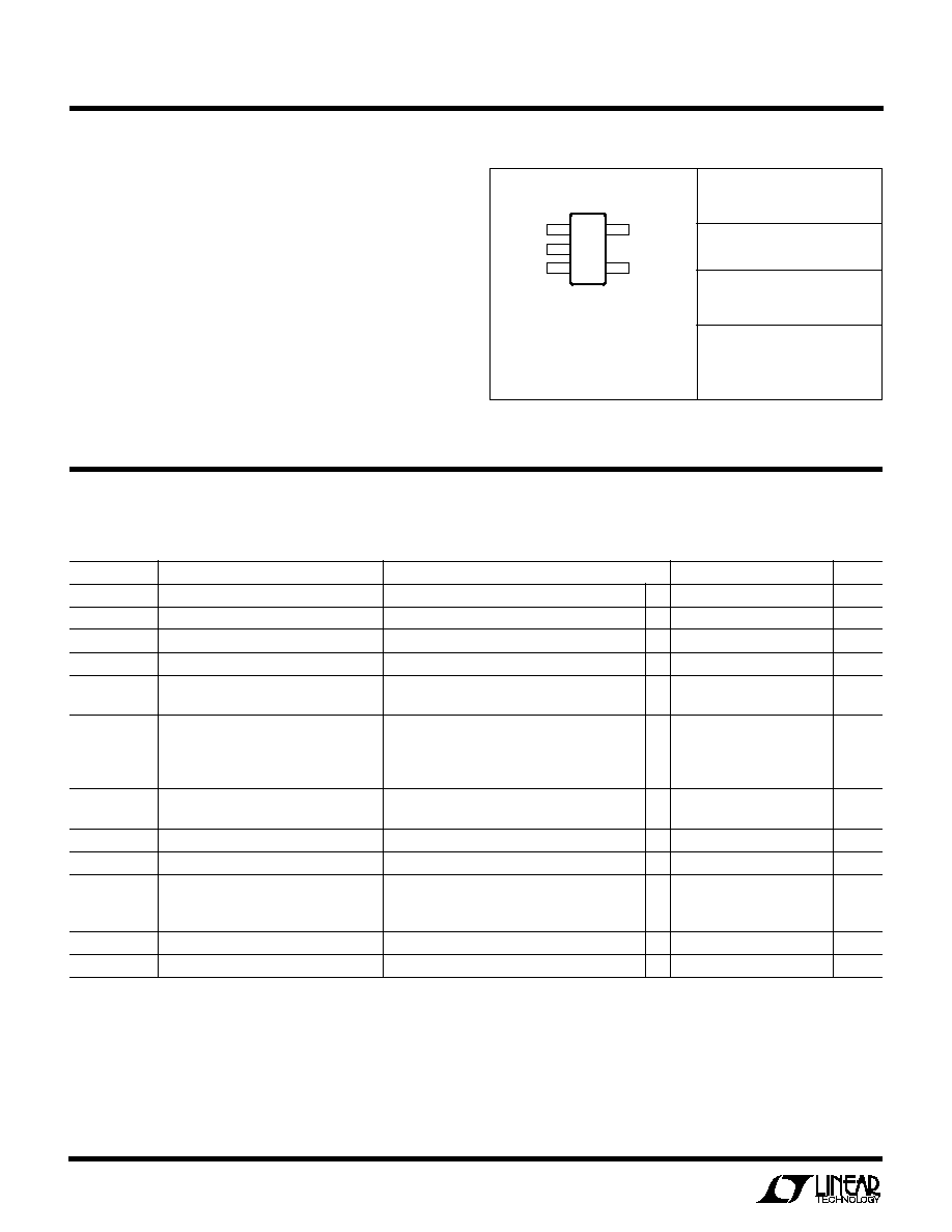
SW 1
GND 2
V
FB
3
5 V
IN
4 I
TH
/RUN
TOP VIEW
S5 PACKAGE
5-LEAD PLASTIC SOT-23
3
LTC1701
SW (Pin 1): The Switch Node Connection to the Inductor.
This pin swings from V
IN
to a Schottky diode (external)
voltage drop below ground. The cathode of the Schottky
diode must be closely connected to this pin.
GND (Pin 2): Ground Pin. Connect to the (≠) terminal of
C
OUT
, the Schottky diode and (≠) terminal of C
IN
.
V
FB
(Pin 3): Receives the feedback voltage from the
external resistive divider across the output. Nominal volt-
age for this pin is 1.25V.
I
TH
/RUN (Pin 4): Combination of Error Amplifier Compen-
sation Point and Run Control Input. The current compara-
tor threshold increases with this control voltage. Nominal
voltage range for this pin is 1.25V to 2.25V. Forcing this
pin below 0.8V causes the device to be shut down. In
shutdown all functions are disabled.
V
IN
(Pin 5): Main Supply Pin and the (+) Input to the
Current Comparator. Must be closely decoupled to ground.
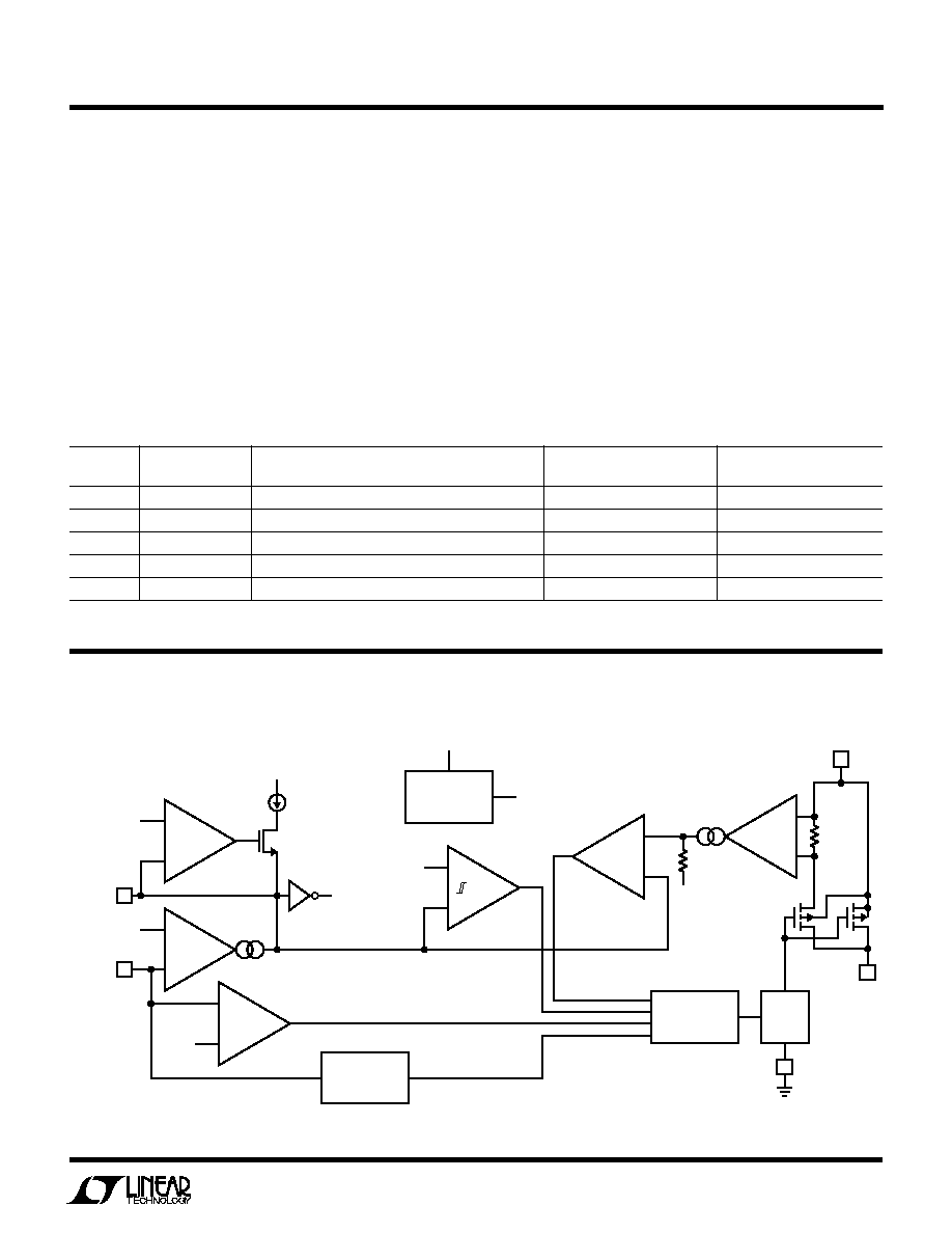
PI FU CTIO S
U
U
U
BLOCK DIAGRA
W
≠
+
1.25V
BANDGAP
REFERENCE
I
TH
/REF
CLAMP
SHDN
50
µ
A
V
REF
V
REF
1.4V
1.5V
V
REF
(1.25V)
≠
+
OVER
VOLTAGE
COMP
≠
+
I
TH
COMP
≠
+
ERROR
AMP
(1.25V TO 2.25V)
≠
+
CURRENT
COMP
V
REF
≠
+
CURRENT
SENSE
AMP
SW
GND
1701 BD
V
IN
OFF-TIMER
AND GATE
CONTROL LOGIC
GATE
DRIVER
V
FB
I
TH
/RUN
PULSE
STRETCHER
V
FB
< 0.6V
V
IN
V
IN
Pin Limit Table
NOMINAL (V)
ABSOLUTE MAX (V)
PIN
NAME
DESCRIPTION
MIN
TYP
MAX
MIN
MAX
1
SW
Switch Node
≠ 0.3
V
IN
≠ 0.3
V
IN
+ 0.3
2
GND
Ground Pin
0
3
V
FB
Output Feedback Pin
0
1.25
1.35
≠ 0.3
3
4
I
TH
/RUN
Error Amplifier Compensation and RUN Pin
0
2.25
≠ 0.3
3
5
V
IN
Main Power Supply
2.5
5.5
≠ 0.3
6
4
LTC1701
OPERATIO
U
The LTC1701 uses a contant off-time, current mode
architecture. The operating frequency is then determined
by the off-time and the difference between V
IN
and V
OUT
.
To optimize efficiency, the LTC1701 automatically switches
between continuous and Burst Mode
operation.
The output voltage is set by an external divider returned to
the V
FB
pin. An error amplfier compares the divided output
voltage with a reference voltage of 1.25V and adjusts the
peak inductor current accordingly.
Main Control Loop
During normal operation, the internal PMOS switch is
turned on when the V
FB
voltage is below the reference
voltage. The current into the inductor and the load in-
creases until the current limit is reached. The switch turns
off and energy stored in the inductor flows through the
external Schottky diode into the load. After the constant
off-time interval, the switch turns on and the cycle repeats.
The peak inductor current is controlled by the voltage on
the I
TH
/RUN pin, which is the output of the error
amplifier.This amplifier compares the V
FB
pin to the 1.25V
reference. When the load current increases, the FB voltage
decreases slightly below the reference. This decrease
causes the error amplifier to increase the I
TH
/RUN voltage
until the average inductor current matches the new load
current.
The main control loop is shut down by pulling the I
TH
/RUN
pin to ground. When the pin is released an external resistor
is used to charge the compensation capacitor. When the
voltage at the I
TH
/RUN pin reaches 0.8V, the main control
loop is enabled and the error amplifier drives the I
TH
/RUN
pin. Soft-start can be implemented by ramping the voltage
on the I
TH
/RUN pin (see Applications Information sec-
tion).
Low Current Operation
When the load is relatively light, the LTC1701 automati-
cally switches to Burst Mode
operation in which the
internal PMOS switch operates intermittently based on
load demand. The main control loop is interrupted when
the output voltage reaches the desired regulated value.
The hysteretic voltage comparator trips when I
TH
/RUN is
below 1.5V, shutting off the switch and reducing the
power consumed. The output capacitor and the inductor
supply the power to the load until the output voltage drops
slightly and the I
TH
/RUN pin exceeds 1.5V, turning on the
switch and the main control loop which starts another
cycle.
Dropout Operation
In dropout, the internal PMOS switch is turned on continu-
ously (100% duty cycle) providing low dropout operation
with V
OUT
at V
IN
. Since the LTC1701 does not incorporate
an under voltage lockout, care should be taken to shut
down the LTC1701 for V
IN
< 2.5V.
APPLICATIO S I FOR ATIO
W
U
U
U
The basic LTC1701 application circuit is shown in
Figure 1. External component selection is driven by the
load requirement and begins with the selection of L1. Once
L1 is chosen, the Schottky diode D1 can be selected
followed by C
IN
and C
OUT
.
L Selection and Operating Frequency
The operating frequency is fixed by V
IN
, V
OUT
and the
constant off-time of about 500ns. The complete expres-
sion for operating frequency is given by:
f
O
=
-
+
V
V
V
V
T
IN
OUT
IN
D
OFF
1
Although the inductor does not influence the operating
frequency, the inductor value has a direct effect on ripple
current. The inductor ripple current
I
L
decreases with
higher inductance and increases with higher V
IN
or V
OUT
:
=
-
+
+
I
V
V
fL
V
V
V
V
L
IN
OUT
OUT
D
IN
D
5
LTC1701
APPLICATIO S I FOR ATIO
W
U
U
U
where V
D
is the output Schottky diode forward drop.
Accepting larger values of
I
L
allows the use of low
inductances, but results in higher output voltage ripple
and greater core losses. A reasonable starting point for
setting ripple current is
I
L
= 0.4A.
The inductor value also has an effect on low current
operation. Lower inductor values (higher
I
L
) will cause
Burst Mode operation to begin at higher load currents,
which can cause a dip in efficiency in the upper range of
low current operation. In Burst Mode operation, lower
inductance values will cause the burst frequency to de-
crease.
Inductor Core Selection
Once the value for L is selected, the type of inductor must
be chosen. Basically, there are two kinds of losses in an
inductor --core and copper losses.
Core losses are dependent on the peak-to-peak ripple
current and core material. However, it is independent of
the physical size of the core. By increasing inductance, the
peak-to-peak inductor ripple current will decrease, there-
fore reducing core loss. Unfortunately, increased induc-
tance requires more turns of wire and, therefore, copper
losses will increase. When space is not a premium, larger
wire can be used to reduce the wire resistance. This also
prevents excessive heat dissipation in the inductor.
High efficiency converters generally cannot afford the core
loss found in low cost powdered iron cores, forcing the
use of more expensive ferrite, molypermalloy or Kool M
µ
Æ
cores. These low core loss materials allow the user to
concentrate on reducing copper loss and preventing satu-
ration.
Ferrite designs have very low core loss and are preferred
at high switching frequencies. Ferrite core material satu-
rates "hard," which means that inductance collapses
abruptly when the peak design current is exceeded. This
results in an abrupt increase in inductor ripple current and
consequent output voltage ripple. Do not allow the core to
saturate!
Molypermalloy (from Magnetics, Inc.) is a very good, low
loss core material for toroids, but it is more expensive than
ferrite. A reasonable compromise from the same manu-
facturer is Kool M
µ
core material. Toroids are very space
efficient, expecially when you can use several layers of
wire. Because they generally lack a bobbin, mounting is
more difficult. However, surface mount designs that do
not increase the height significantly are available
Catch Diode Selection
The diode D1 shown in Figure 1 conducts during the off-
time. It is important to adequately specify the diode peak
current and average power dissipation so as not to exceed
the diode ratings.
Losses in the catch diode depend on forward drop and
switching times. Therefore, Schottky diodes are a good
choice for low drop and fast switching times.
Since the catch diode carries the load current during the
off-time, the average diode current is dependent on the
switch duty cycle. At high input voltages, the diode con-
ducts most of the time. As V
IN
approaches V
OUT
, the diode
conducts only a small fraction of the time. The most
stressful condition for the diode is when the regulator
output is shorted to ground.
Under short-circuit conditions (V
OUT
= 0V), the diode
must safely handle I
SC(PK)
at close to 100% duty cycle.
Under normal load conditions, the average current con-
ducted by the diode is simply:
I
I
V
V
V
V
DIODE avg
LOAD avg
IN
OUT
IN
D
(
)
(
)
=
-
+
Remember to keep lead lengths short and observe proper
grounding (see Board Layout Considerations) to avoid
ringing and increased dissipation.
The forward voltage drop allowed in the diode is calculated
from the maximum short-circuit current as:
V
P
I
V
V
V
D
D
SC avg
IN
D
IN
+
(
)
where P
D
is the allowable diode power dissipation and will
be determined by efficiency and/or thermal requirements
(see Efficiency Considerations).
Kool M
µ
is a registered trademark of Magnetics, Inc.
6
LTC1701
Most LTC1701 circuits will be well served by either an
MBR0520L or an MBRM120L. An MBR0520L is a good
choice for I
OUT(MAX)
500mA, as long as the output
doesn't need to sustain a continuous short.
Input Capacitor (C
IN
) Selection
In continuous mode, the input current of the converter is
a square wave with a duty cycle of approximately V
OUT
/
V
IN
. To prevent large voltage transients, a low equivalent
series resistance (ESR) input capacitor sized for the maxi-
mum RMS current must be used. The maximum RMS
capacitor current is given by:
I
I
V
V
V
V
RMS
MAX
OUT
IN
OUT
IN
-
(
)
where the maximum average output current I
MAX
equals
the peak current (1 Amp) minus half the peak-to-peak
ripple current, I
MAX
= 1 ≠
I
L
/2.
This formula has a maximum at V
IN
= 2V
OUT
, where I
RMS
= I
OUT
/2. This simple worst-case is commonly used to
design because even significant deviations do not offer
much relief. Note that capacitor manufacturer's ripple
current ratings are often based on only 2000 hours life-
time. This makes it advisable to further derate the capaci-
tor, or choose a capacitor rated at a higher temperature
than required. Several capacitors may also be paralleled to
meet the size or height requirements of the design. An
additional 0.1
µ
F to 1
µ
F ceramic capacitor is also recom-
mended on V
IN
for high frequency decoupling.
Output Capacitor (C
OUT
) Selection
The selection of C
OUT
is driven by the required ESR.
Typically, once the ESR requirement is satisfied, the
capacitance is adequate for filtering. The output ripple
(
V
OUT
) is determined by:
+
V
I ESR
fC
OUT
L
OUT
1
8
where f = operating frequency, C
OUT
= output capacitance
and
I
L
= ripple current in the inductor. With
I
L
= 0.4
I
OUT(MAX)
the output ripple will be less than 100mV with:
ESR
COUT
< 100m
Once the ESR requirements for C
OUT
have been met, the
RMS current rating generally far exceeds the I
RIPPLE(P-P)
requirement.
When the capacitance of C
OUT
is made too small, the
output ripple at low frequencies will be large enough to trip
the I
TH
comparator. This causes Burst Mode operation to
be activated when the LTC1701 would normally be in
continuous mode operation. The effect can be improved at
higher frequencies with lower inductor values.
In surface mount applications, multiple capacitors may
have to be paralleled to meet the capacitance, ESR or RMS
current handling requirement of the application. Alumi-
num electrolyte and dry tantulum capacitors are both
available in surface mount configurations. The OS-CON
semiconductor dielectric capacitor available from Sanyo
has the lowest ESR(size) product of any aluminum elec-
trolytic at a somewhat higher price. In the case of tanta-
lum, it is critical that the capacitors are surge tested for use
in switching power supplies. An excellent choice is the
AVX TPS, AVX TPSV and KEMET T510 series of surface
mount tantalums, avalable in case heights ranging from
2mm to 4mm. Other capacitor types include Nichicon PL
series, Sanyo POSCAP and Panasonic SP.
Ceramic Capacitors
Higher value, lower cost ceramic capacitors are now
becoming available in smaller case sizes. These are tempt-
ing for switching regulator use because of their very low
ESR. Unfortunately, the ESR is so low that it can cause
loop stability problems. Solid tantalum capacitor ESR
generates a loop "zero" at 5kHz to 50kHz that is instrumen-
tal in giving acceptable loop phase margin. Ceramic ca-
pacitors remain capacitive to beyond 300kHz and usually
resonate with their ESL before ESR becomes effective.
Also, ceramic caps are prone to temperature effects which
requires the designer to check loop stability over the
operating temperature range.
For these reasons, most of the input and output capaci-
tance should be composed of tantalum capacitors for
stability combined with about 0.1
µ
F to 1
µ
F of ceramic
capacitors for high frequency decoupling.
APPLICATIO S I FOR ATIO
W
U
U
U
7
LTC1701
Setting the Output Voltage
The LTC1701 develops a 1.25V reference voltage between
the feedback pin, V
FB
, and the signal ground as shown in
Figure 2. The output voltage is set by a resistive divider
according to the following formula:
V
V
R
R
OUT
=
+
1 25
1
2
1
.
To prevent stray pickup, a capacitor of about 5pF can be
added across R1, located close to the LTC1701. Unfortu-
nately, the load step response is degraded by this capaci-
tor. Using a good printed circuit board layout eliminates
the need for this capacitor. Great care should be taken to
route the V
FB
line away from noise sources, such as the
inductor or the SW line.
APPLICATIO S I FOR ATIO
W
U
U
U
V
FB
SGND
LTC1701
R2
1%
R1
100k
1%
1701 F02
V
OUT
C
F
5pF
Transient Response
The OPTI-LOOP compensation allows the transient re-
sponse to be optimized for a wide range of loads and
output capacitors. The availability of the I
TH
pin not only
allows optimization of the control loop behavior but also
provides a DC coupled and AC filtered closed-loop re-
sponse test point. The DC step, rise time and settling at this
test point truly reflects the closed-loop response. Assum-
ing a predominately second order system, phase margin
and/or damping factor can be estimated using the percent-
age of overshoot seen at this pin. The bandwidth can also
be estimated by examining the rise time at the pin.
The I
TH
external components shown in the Figure 1 circuit
will provide an adequate starting point for most applica-
tions. The series R3-C3 filter sets the dominant pole-zero
loop compensation. The values can be modified slightly
Figure 2. Setting the Output Voltage
(from 0.5 to 2 times their suggested values) to optimize
transient response once the final PC layout is done and the
particular output capacitor type and value have been
determined. The output capacitors need to be selected
because the various types and values determine the loop
feedback factor gain and phrase. An output current pulse
of 20% to 100% of full-load current having a rise time of
1
µ
s to 10
µ
s will produce output voltage and I
TH
pin
waveforms that will give a sense of the overall loop
stability without breaking the feedback loop.
The initial output voltage step may not be within the
bandwidth of the feedback loop, so the standard second-
order overshoot/DC ratio cannot be used to determine
phase margin. The gain of the loop increases with R3 and
the bandwidth of the loop increases with decreasing C3. If
R3 is increased by the same factor that C3 is decreased,
the zero frequency will be kept the same, thereby keeping
the phase the same in the most critical frequency range of
the feedback loop. In addition, a feed-forward capacitor,
C
F
, can be added to improve the high frequency response,
as shown in Figure 2. Capacitor C
F
provides phase lead by
creating a high frequency zero with R2 which improves the
phase margin.
The output voltage settling behavior is related to the
stability of the closed-loop system and will demonstrate
the actual overall supply performance. For a detailed
explanation of optimizing the compensation components,
including a review of control loop theory, refer to Applica-
tion Note 76.
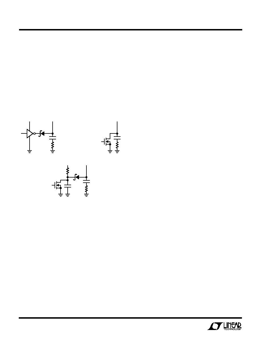
RUN Function
The I
TH
/RUN pin is a dual purpose pin that provides the
loop compensation and a means to shut down the LTC1701.
Soft-start can also be implemented with this pin. Soft-start
reduces surge currents from V
IN
by gradually increasing
the internal peak inductor current. Power supply sequenc-
ing can also be accomplished using this pin.
An external pull-up is required to charge the external
capacitor C3 in Figure 1. Typically, a 1M resistor between
V
IN
and I
TH
/RUN is used. When the voltage on I
TH
/RUN
reaches about 0.8V the LTC1701 begins operating. At this
point the error amplifier pulls up the I
TH
/RUN pin to the
normal operating range of 1.25V to 2.25V.
8
LTC1701
APPLICATIO S I FOR ATIO
W
U
U
U
Soft-start can be implemented by ramping the voltage on
I
TH
/RUN during start-up as shown in Figure 3(c). As the
voltage on I
TH
/RUN ramps through its operating range the
internal peak current limit is also ramped at a proportional
linear rate.
During normal operation the voltage on the I
TH
/RUN pin
will vary from 1.25V to 2.25V depending on the load
current. Pulling the I
TH
/RUN pin below 0.8V puts the
LTC1701 into a low quiescent current shutdown mode
(I
Q
< 1
µ
A). This pin can be driven directly from logic as
shown in Figures 3(a) and 3(b).
1) The V
IN
current is the DC supply current given in the
electrical characteristics which excludes MOSFET driver
and control currents. V
IN
current results in a small (< 0.1%)
loss that increases with V
IN
, even at no load.
2) The switching current is the sum of the internal MOSFET
driver and control currents. The MOSFET driver current
results from switching the gate capacitance of the power
MOSFET. Each time a MOSFET gate is switched from low
to high to low again, a packet of charge dQ moves from V
IN
to ground. The resulting dQ/dt is a current out of V
IN
that
is typically much larger than the control circuit current. In
continuous mode, I
GATECHG
= f ∑ Q
P
, where Q
P
is the gate
charge of the internal MOSFET switch.
3) I
2
R Losses are predicted from the DC resistances of the
MOSFET and inductor. In continuous mode the average
output current flows through L, but is "chopped" between
the topside internal MOSFET and the Schottky diode. At
low supply voltages where the switch on-resistance is
higher and the switch is on for longer periods due to the
higher duty cycle, the switch losses will dominate. Using
a larger inductance helps minimize these switch losses. At
high supply voltages, these losses are proportional to the
load. I
2
R losses cause the efficiency to drop at high output
currents.
4) The Schottky diode is a major source of power loss at
high currents and gets worse at low output voltages. The
diode loss is calculated by multiplying the forward voltage
drop times the diode duty cycle multiplied by the load
current.
Other "hidden" losses such as copper trace and internal
battery resistances can account for additional efficiency
degradations in portable systems. It is very important to
include these "system" level losses in the design of a
system. The internal battery and fuse resistance losses
can be minimized by making sure that C
IN
has adequate
charge storage and very low ESR at the switching fre-
quency. Other losses including Schottky conduction losses
during dead-time and inductor core losses generally ac-
count for less than 2% total additional loss.
3.3V OR 5V
I
TH
/RUN
D1
D1
C
C
R
C
I
TH
/RUN
C
C
R
C
1701 F03
I
TH
/RUN
C
C
R
C
C1
R1
(a)
(b)
(c)
Figure 3. I
TH
/RUN Pin Interfacing
Efficiency Considerations
The percent efficiency of a switching regulator is equal to
the output power divided by the input power times 100%.
It is often useful to analyze individual losses to determine
what is limiting the efficiency and what change would
produce the most improvement. Percent efficiency can be
expressed as:
%Efficiency = 100% ≠ (L1 + L2 + L3 + ...)
where L1, L2, etc. are the individual losses as a percentage
of input power.
Although all dissipative elements in the circuit produce
losses, 4 main sources usually account for most of the
losses in LTC1701 circuits: 1) LTC1701 V
IN
current,
2) switching losses, 3) I
2
R losses, 4) Schottky diode
losses.
9
LTC1701
APPLICATIO S I FOR ATIO
W
U
U
U
THERMAL CONSIDERATIONS
The power handling capability of the device at high ambi-
ent temperatures will be limited by the maximum rated
junction temperature (125
∞
C). It is important to give
careful consideration to all sources of thermal resistance
from junction to ambient. Additional heat sources mounted
nearby must also be considered.
For surface mount devices, heat sinking is accomplished
by using the heat spreading capabilities of the PC board
and its copper traces. Copper board stiffeners and plated
through-holes can also be used to spread the heat gener-
ated by power devices.
The following table lists thermal resistance for several
different board sizes and copper areas. All measurements
were taken in still air on 3/32" FR-4 board with one ounce
copper.
Table 1. Measured Thermal Resistance
COPPER AREA
THERMAL RESISTANCE
TOPSIDE*
BACKSIDE
BOARD AREA
JA
2500mm
2
2500mm
2
2500mm
2
125
∞
C/W
1000mm
2
2500mm
2
2500mm
2
125
∞
C/W
225mm
2
2500mm
2
2500mm
2
130
∞
C/W
100mm
2
2500mm
2
2500mm
2
135
∞
C/W
50mm
2
2500mm
2
2500mm
2
150
∞
C/W
*Device is mounted on topside.
Calculating Junction Temperature
In a majority of applications, the LTC1701 does not
dissipate much heat due to its high efficiency. However, in
applications where the switching regulator is running at
high duty cycles or the part is in dropout with the switch
turned on continuously (DC), some thermal analysis is
required. The goal of the thermal analysis is to determine
whether the power dissipated by the regulator exceeds the
maximum junction temperature. The temperature rise is
given by:
T
RISE
= P
D
∑
JA
where P
D
is the power dissipated by the regulator and
JA
is the thermal resistance from the junction of the die to the
ambient temperature.
The junction temperature is given by:
T
J
= T
RISE
+ T
AMBIENT
As an example, consider the case when the LTC1701 is in
dropout at an input voltage of 3.3V with a load current of
0.5A. The ON resistance of the P-channel switch is ap-
proximately 0.30
. Therefore, power dissipated by the
part is:
P
D
= I
2
∑ R
DS(ON)
= 75mW
The SOT package junction-to-ambient thermal resistance,
JA
, will be in the range of 125
∞
C/W to 150
∞
C/W. There-
fore, the junction temperature of the regulator operating in
a 25
∞
C ambient temperature is approximately:
T
J
= 0.075 ∑ 150 + 25 = 36
∞
C
Remembering that the above junction temperature is
obtained from a R
DS(ON)
at 25
∞
C, we might recalculate the
junction temperature based on a higher R
DS(ON)
since it
increases with temperature. However, we can safely as-
sume that the actual junction temperature will not exceed
the absolute maximum junction temperature of 125
∞
C.
Board Layout Considerations
When laying out the printed circuit board, the following
checklist should be used to ensure proper operation of the
LTC1701. These items are also illustrated graphically in
the layout diagram of Figure 4. Check the following in your
layout:
1. Does the capacitor C
IN
connect to the power V
IN
(Pin 5)
and GND (Pin 2) as close as possible? This capacitor
provides the AC current to the internal P-channel MOSFET
and its driver.
2. Is the Schottky diode closely connected between the
ground (Pin 2) and switch output (Pin 1)?
3. Are the C
OUT
, L1 and D1 closely connected? The
Schottky anode should connect directly to the input ca-
pacitor ground.
4. The resistor divider, R1 and R2, must be connected
between the (+) plate of C
OUT
and a ground line terminated
near GND (Pin 2). The feedback signal FB should be routed
away from noisy components and traces, such as the SW
line (Pin 1).
10
LTC1701
TYPICAL APPLICATIO S
U
V
IN
I
TH
/RUN
SW
V
FB
GND
C4
0.1
µ
F
+
R3
5.1k
R4
1M
R1
121k
D1
C3
330pF
C1
15
µ
F
+
C2
15
µ
F
R2
121k
L1
4.7
µ
H
V
IN
2.7V TO 5.5V
V
OUT
(2.5V/0.5A)
LTC1701
C1, C2: AVX TAJA156M010R
C4: TAIYO YUDEN EMK107BJ104MA
D1: MBR0520
L1: MURATA LQH3C4R7M24 OR TAIYO YUDEN LEMC3225B4R7M
1701 TA01
V
IN
I
TH
/RUN
SW
V
FB
GND
C4
1
µ
F
+
R3
5.1k
R4
1M
R1
100k
D1
C3
330pF
C1
15
µ
F
C5
4.7
µ
F
+
C2
22
µ
F
R2
20k
L1
4.7
µ
H
V
IN
2.5V TO 5.5V
V
OUT
(1.5V/0.5A)
LTC1701
C1: AVX TAJA156M010R
C2: AVX TAJA226M006R
C4: TAIYO YUDEN LMK212BJ105MG
C5: TAIYO YUDEN JMK212BJ475MG
D1: MBRM120L
L1: MURATA LQH3C4R7M24
1701 TA02
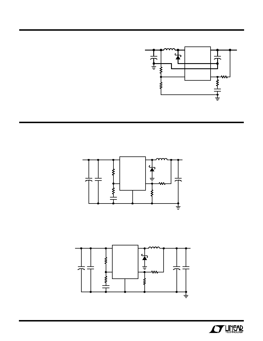
3- to 4-Cell NiCd/NiMH to 2.5V Converter
2mm Nominal Height 1.5V Converter
5. Keep sensitive components away from the SW pin. The
input capacitor C
IN
, the compensation capacitor C
C
and all
the resistors R1, R2, R
C
and R
S
should be routed away
from the SW trace and the components L1 and D1.
SW
V
FB
V
IN
I
TH
/RUN
GND
LTC1701
D1
L1
R2
R1
C
OUT
1701 F04
V
OUT
V
IN
1
2
3
5
4
C
IN
C
C
R
C
R
S
BOLD LINES INDICATE HIGH CURRENT PATHS
+
+
Figure 4. LTC1701 Layout Diagram (See Board Layout Checklist)
APPLICATIO S I FOR ATIO
W
U
U
U
11
LTC1701
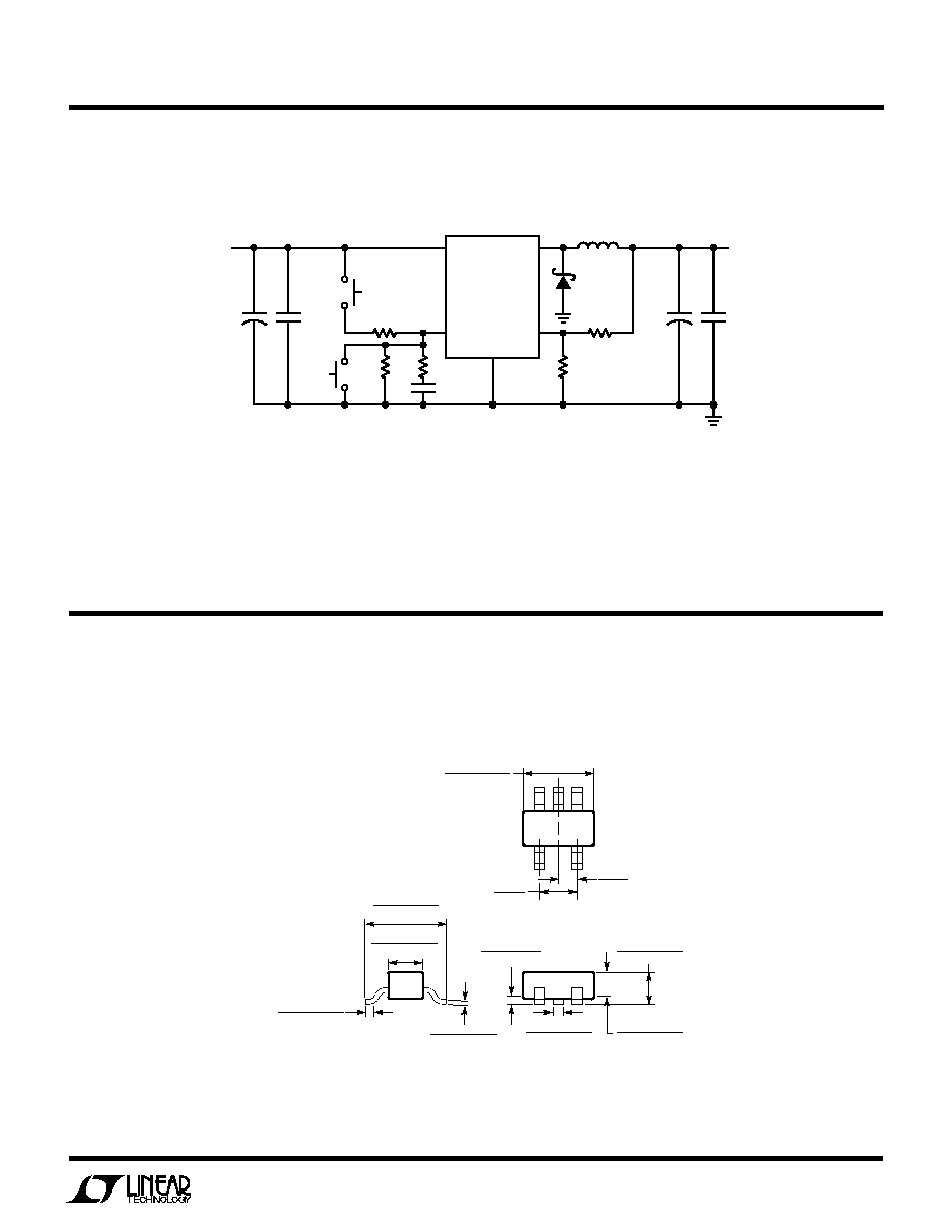
V
IN
I
TH
/RUN
SW
V
FB
GND
C4
1
µ
F
+
R3
5.1k
R5
5.1M
R1
20.5k
D1
C3
330pF
C1
15
µ
F
C5
4.7
µ
F
+
C2
22
µ
F
R2
34k
R4
1M
L1
4.7
µ
H
V
IN
5V
V
OUT
(3.3V/0.5A)
LTC1701
C1: AVX TAJA156M010R
C2: AVX TAJA226M006R
C4: TAIYO YUDEN LMK212BJ105MG
C5: TAIYO YUDEN JMK212BJ475MG
D1: MBRM120L
L1: MURATA LQH3C4R7M24
1701 TA03
ON
OFF
Dimensions in inches (millimeters) unless otherwise noted.
PACKAGE DESCRIPTIO
U
0.95
(0.037)
REF
1.50 ≠ 1.75
(0.059 ≠ 0.069)
0.35 ≠ 0.55
(0.014 ≠ 0.022)
0.35 ≠ 0.50
(0.014 ≠ 0.020)
FIVE PLACES (NOTE 2)
S5 SOT-23 0599
2.80 ≠ 3.00
(0.110 ≠ 0.118)
(NOTE 3)
1.90
(0.074)
REF
0.90 ≠ 1.45
(0.035 ≠ 0.057)
0.90 ≠ 1.30
(0.035 ≠ 0.051)
0.00 ≠ 0.15
(0.00 ≠ 0.006)
0.09 ≠ 0.20
(0.004 ≠ 0.008)
(NOTE 2)
2.60 ≠ 3.00
(0.102 ≠ 0.118)
NOTE:
1. DIMENSIONS ARE IN MILLIMETERS
2. DIMENSIONS ARE INCLUSIVE OF PLATING
3. DIMENSIONS ARE EXCLUSIVE OF MOLD FLASH AND METAL BURR
4. MOLD FLASH SHALL NOT EXCEED 0.254mm
5. PACKAGE EIAJ REFERENCE IS SC-74A (EIAJ)
S5 Package
5-Lead Plastic SOT-23
(LTC DWG # 05-08-1633)
5V to 3.3V Converter with Push-Button On/Off
TYPICAL APPLICATIO S
U
12
LTC1701
Linear Technology Corporation
1630 McCarthy Blvd., Milpitas, CA 95035-7417
(408) 432-1900
q
FAX: (408) 434-0507
q
www.linear-tech.com
©
LINEAR TECHNOLOGY CORPORATION 1999
1701i LT/TP 1299 4K ∑ PRINTED IN USA
PART NUMBER
DESCRIPTION
COMMENTS
LTC1174/LTC1174-3.3/
High Efficiency Step-Down and Inverting DC/DC Converter
Monolithic Switching Regulator, Burst Mode Operation,
LTC1174-5
I
OUT
Up to 300mA, SO-8
LTC1265
1.2A, High Efficiency Step-Down DC/DC Converter
Monolithic, Burst Mode Operation, High Efficiency
LT1375/LT1376
1.5A, 500kHz Step-Down Switching Regulator
High Frequency, Small Inductor, High Efficiency, SO-8
LTC1435/LTC1435A
High Efficiency, Low Noise, Synchronous Step-Down Converter
3.5V
V
IN
36V, 16-Pin Narrow SO and SSOP
LTC1474/LTC1475
Low Quiescent Current High Efficiency Step-Down Converter
10
µ
A I
Q
, 8-Pin MSOP and SO Packages
LTC1622
Low Input Voltage Current Mode Step-Down DC/DC Controller
High Frequency, High Efficiency, 8-Pin MSOP
LTC1627
Monolithic Synchronous Step-Down Switching Regulator
SO-8, 2.65V
V
IN
10V, I
OUT
Up to 500mA
LTC1707
Monolithic Synchronous Step-Down Switching Regulator
SO-8, 2.95V
V
IN
10V, V
REF
Output
LTC1772
Low Input Voltage Current Mode Step-Down DC/DC Controller
550kHz, 6-Pin SOT-23, I
OUT
Up to 5A, 2.2V < V
IN
< 10V
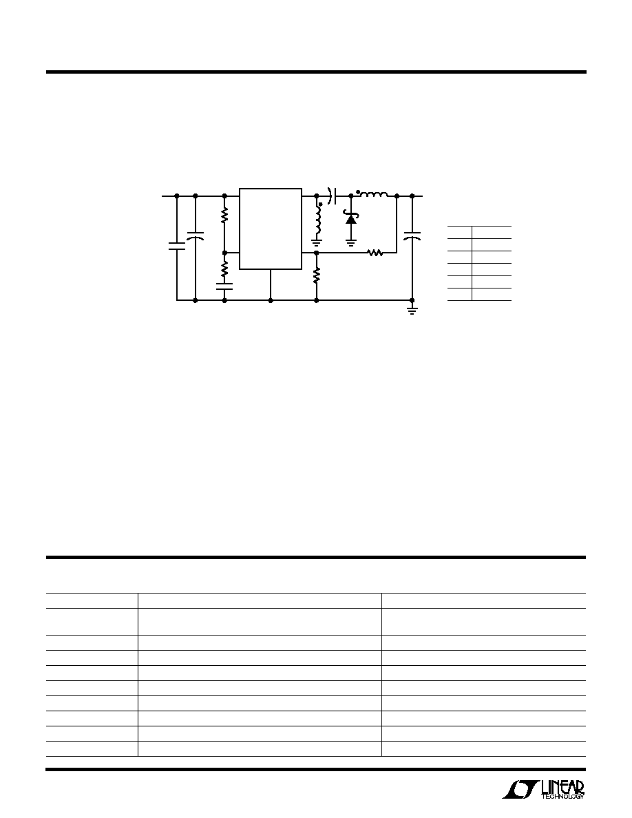
RELATED PARTS
+
+
V
IN
I
TH
/RUN
SW
V
FB
GND
C2
15
µ
F
+
C1
33
µ
F
R3
5.1k
R4
1M
R1
20.5k
L2
D1
C3
330pF
C4
1
µ
F
CERAMIC
R2
34k
L1
4.7
µ
H
C6
4.7
µ
F
V
IN
2.5V TO 4.2V
V
OUT
(3.3V)
LTC1701
C1: AVX TPSB336K006R0600
C2: TAJA156M010R
C6: TAIYO YUDEN JMK212BJ475MG
D1: MBR0520L
L1, L2: COILTRONICS CTX5-1
1701 TA04
V
IN
I
OUT(MAX)
2.5V
200mA
3.0V
225mA
3.5V
250mA
4.0V
280mA
4.2V
290mA
Single Cell Li-Ion to 3.3V Buck Boost Converter
TYPICAL APPLICATIO
U