1
LTC1706-61
170661f
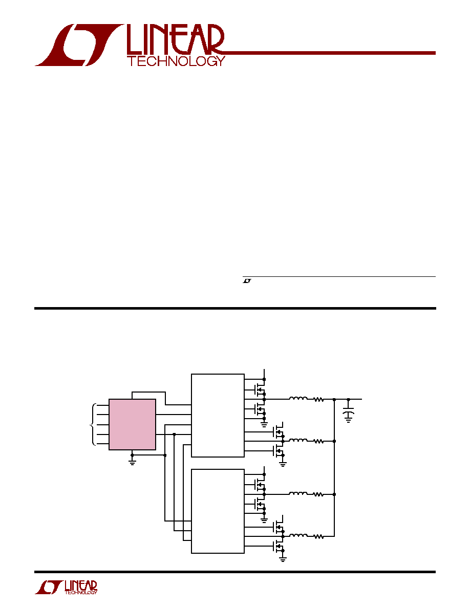
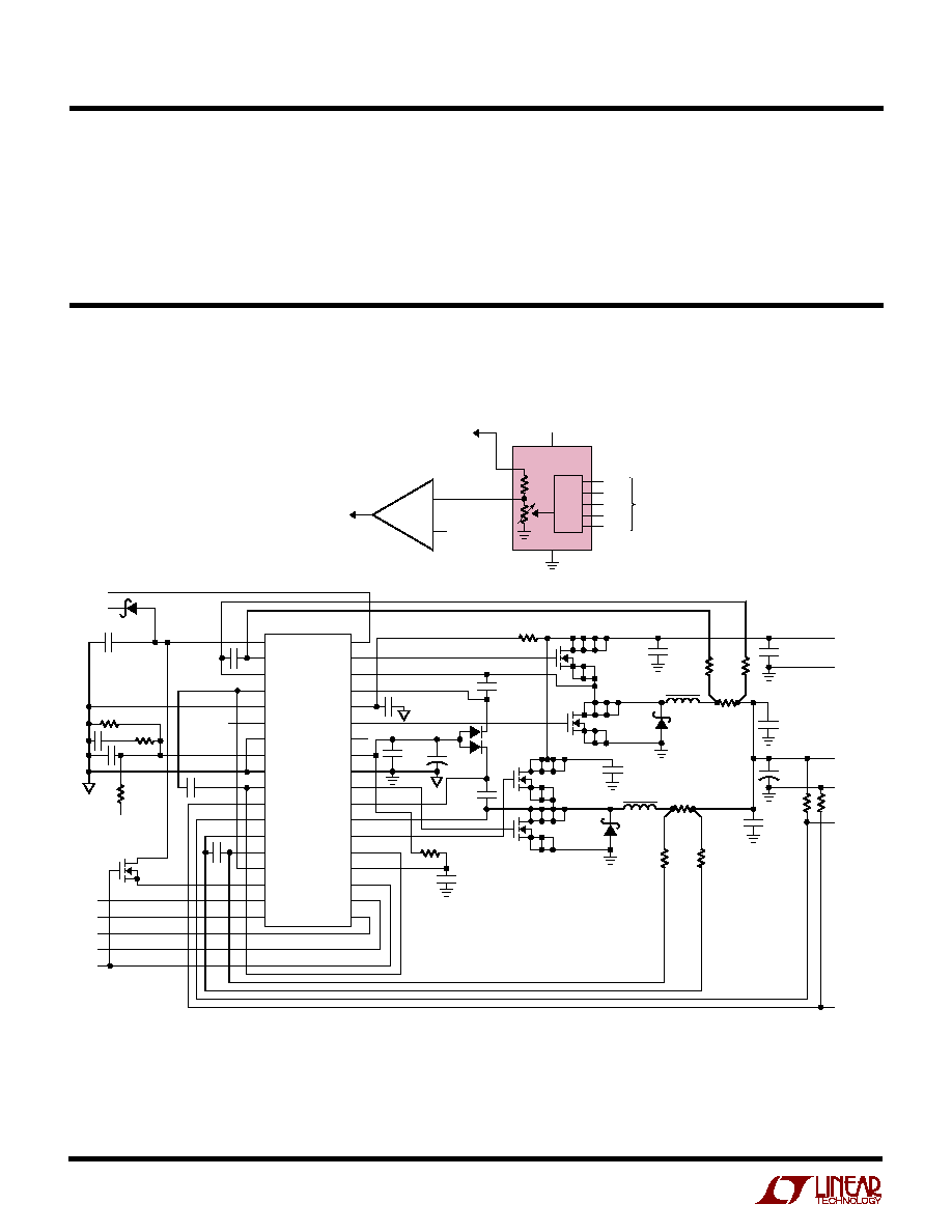
5-Bit VID-Controlled High Current Application (Simplified Block Diagram)
5-Bit VID Voltage
Programmer for AMD
Opteron CPUs
s
Programs Regulator Output Voltage Range from
0.8V to 1.55V in 25mV Steps
s
Programs a Wide Range of Linear Technology
DC/DC Converters with a 0.6V Reference
s
±
0.35% Accurate Output Voltage
s
Built-In 40k Pull-Up Resistors on VID Inputs
s
Available in MSOP-10 Package
The LTC
Æ
1706-61 is a precision, digitally programmed,
resistive ladder which adjusts the output of any 0.6V
referenced regulator. Depending on the state of the five
VID inputs, an output voltage between 0.8V and 1.55V is
programmed in 25mV increments.
The LTC1706-61 is designed specifically to program
an entire family of Linear Technology DC/DC converters
with on board 0.6V references.
The LTC1706-61 programs the following Linear
Technology DC/DC converter products: LTC1629-6,
LTC3714, LTC3731 and LTC3778. (Consult factory for
additional DC/DC converter products.)
s
AMD Opteron
TM
Processor Power Supply
s
Workstations and Servers
s
Large Memory Array Supply
, LTC and LT are registered trademarks of Linear Technology Corporation.
1706-61 TA01
L1
R
SENSE1
V
IN
V
IN
4.5V TO 22V
V
IN
4.5V TO 22V
LTC1629-6
INTV
CC
V
DIFFOUT
SGND
EAIN
I
TH
C
OUT
V
IN
TG1
SW1
BG1
PGND
+
V
OUT
0.8V TO 1.55V
UP TO 80A
VID0
VID1
VID2
VID3
VID4
V
CC
LTC1706-61
GND
SENSE
FB
FROM
µ
P
L2
R
SENSE2
L3
R
SENSE3
V
IN
LTC1629-6
SGND
EAIN
I
TH
V
IN
TG1
SW1
BG1
PGND
L4
R
SENSE4
TG2
SW2
BG2
TG2
SW2
BG2
DESCRIPTIO
U
FEATURES
APPLICATIO S
U
TYPICAL APPLICATIO
U
AMD Opteron is a trademark of Advanced Micro Devices, Inc.

2
LTC1706-61
170661f
Note 1: Absolute Maximum Ratings are those values beyond which the life
of a device may be impaired.
Note 2: The LTC1706EMS-61 is guaranteed to meet performance
specifications from 0
∞
C to 70
∞
C. Specifications over the ≠ 40
∞
C to 85
∞
C
operating temperature range are assured by design, characterization and
correlation with statistical process controls.
SYMBOL
PARAMETER
CONDITIONS
MIN
TYP
MAX
UNITS
V
CC
Operating Supply Voltage Range
2.7
5.5
V
I
VCC
Supply Current
(Note 3)
0.1
5
µ
A
R
FB-SENSE
Resistance Between SENSE and FB
q
6
10
14
k
V
OUT
Error %
Output Voltage Accuracy
q
≠ 0.35
+ 0.35
%
R
PULLUP
VID Input Pull-Up Resistance
V
DIODE
= 0.6V (Note 4)
40
k
VID
TH
VID Input Voltage Threshold
V
IL
(2.7V
V
CC
5.5V)
0.4
V
V
IH
(2.7V
V
CC
5.5V)
1.6
V
I
VID-LEAK
VID Input Leakage Current
V
CC
< VID < 7V (Note 4)
0.01
±
1
µ
A
V
PULLUP
VID Pull-Up Voltage
V
CC
= 3.3V
2.8
V
V
CC
= 5V
4.5
V
LTC1706EMS-61
T
JMAX
= 110
∞
C,
JA
= 120
∞
C/ W
(Note 1)
ABSOLUTE
M
AXI
M
U
M
RATINGS
W
W
W
U
PACKAGE/ORDER I
N
FOR
M
ATIO
N
W
U
U
ELECTRICAL CHARACTERISTICS
Consult LTC Marketing for parts specified with wider operating temperature ranges.
The
q
denotes specifications which apply over the full operating temperature range, otherwise specifications are TA = 25
∞
C.
2.7V
V
CC
5.5V, VID0 = VID1 = VID2 = VID3 = VID4 = NC unless otherwise specified.
(Voltages Referred to GND Pin)
Input Supply Voltage (V
CC
) .......................... ≠ 0.3V to 7V
VID Input Pins .............................................≠ 0.3V to 7V
SENSE Pin ...................................................≠ 0.3V to 7V
FB Pin .......................................................... ≠ 0.3V to 7V
Operating Ambient Temperature Range
(Note 2) .................................................. ≠ 40
∞
C to 85
∞
C
Junction Temperature ........................................... 110
∞
C
Storage Temperature Range ................. ≠ 65
∞
C to 150
∞
C
Lead Temperature (Soldering, 10 sec).................. 300
∞
C
1
2
3
4
5
VID0
VID1
VID2
VID3
V
CC
10
9
8
7
6
FB
GND
NC
VID4
SENSE
TOP VIEW
MS PACKAGE
10-LEAD PLASTIC MSOP
ORDER PART
NUMBER
MS
PART MARKING
LTK9
Note 3: With all five VID inputs floating, the V
CC
supply current is simply
the device leakage current. However, the V
CC
supply current will rise and
be approximately equal to the number of grounded VID input pins times
(V
CC
≠ 0.6V)/40k. (See the VID Input Characteristics section for more
details.)
Note 4: Each built-in pull-up resistor attached to the VID inputs also has a
series diode connected to V
CC
to allow input voltages higher than the V
CC
supply without damage or clamping. (See Operation section for further
details.)
3
LTC1706-61
170661f
TYPICAL PERFOR
M
A
N
CE CHARACTERISTICS
U
W
TEMPERATURE (
∞
C)
≠50
0
50
100
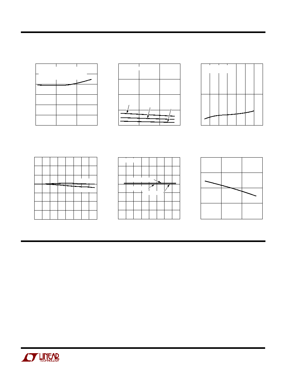
VID PULL-UP CURRENT (
µ
A)
1706-61 G01
140
120
100
80
60
40
20
V
CC
= 5V
VID4 = 0V
VID0 = VID1 = VID2 = VID3 = OPEN
I
VID-PULLUP
vs Temperature
TEMPERATURE (
∞
C)
≠50
0
50
100
SUPPLY CURRENT (
µ
A)
1706-61 G02
2.0
1.5
1.0
0.5
0
V
CC
= 2.7V
V
CC
= 5V
ALL VID INPUTS OPEN
V
CC
= 3.3V
Supply Current vs Temperature
Supply Current vs Supply Voltage
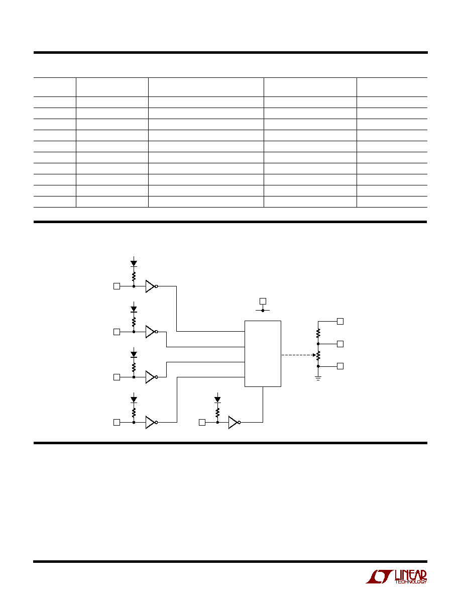
VID0 (Pin 1): LSB Programming Input. Low = GND,
High = V
CC
or Float. Grounding VID0 adds 25mV
to the output sense voltage.
VID1 (Pin 2): 4th MSB Programming Input. Low = GND,
High = V
CC
or Float. Grounding VID1 adds 50mV
to the output sense voltage.
VID2 (Pin 3): 3rd MSB Programming Input. Low = GND,
High = V
CC
or Float. Grounding VID2 adds 100mV
to the output sense voltage.
VID3 (Pin 4): 2nd MSB Programming Input. Low = GND,
High = V
CC
or Float. Grounding VID3 adds 200mV
to the output sense voltage.
V
CC
(Pin 5): Power Supply Voltage. Range from 2.7V to
5.5V.
SENSE (Pin 6): Regulator Output Voltage. Connect
directly to regulator output sense node.
VID4 (Pin 7): MSB Programming Input. Low = GND, High
= V
CC
or Float. Grounding VID4 adds 400mV to the output
sense voltage.
NC (Pin 8): No Connect.
GND (Pin 9): Ground. Connect to regulator signal ground.
FB (Pin 10): Feedback Input. Connect to the 0.6V feedback
pin of a compatible regulator.
PI
N
FU
N
CTIO
N
S
U
U
U
SENSE VOLTAGE (V)
0.775
VID
ACCURACY
(%
)
1706-61 G04
0.35
0.25
0.15
0.05
≠0.05
≠0.15
≠0.25
≠0.35
0.975
1.175
1.375
1.575
V
CC
= 5.5V
V
CC
= 2.7V
TEMPERATURE (
∞
C)
≠60
VID
ACCURACY
(%
)
60
1706-61 G05
≠20
20
100
0.35
0.25
0.15
0.05
≠0.05
≠0.15
≠0.25
≠0.35
≠40
0
40
80
V
CC
= 5.5V
V
SENSE
= 1.15V
V
SENSE
= 0.8V
V
SENSE
= 1.55V
VID
VID Sense Accuracy
VID Sense Accuracy vs
Temperature
R
FB1
vs Temperature
SUPPLY VOLTAGE (V)
2.5
4.5
3.5
3.0
4.0
5.0
5.5
6.0
SUPPLY CURRENT (
µ
A)
1706-61 G03
1.0
0.5
0
ALL VID INPUTS OPEN
T
A
= 25
∞
C
TEMPERATURE (
∞
C)
≠50
0
50
100
R
FB1
(k
)
1706-61 G06
10.10
10.05
10.00
9.95
9.90
4
LTC1706-61
170661f
BLOCK DIAGRA
W
1706-61 BD
40k
VID3
V
CC
40k
VID4
V
CC
40k
VID2
V
CC
40k
VID1
V
CC
40k
VID0
V
CC
R
FB2
R
FB1
SENSE
FB
GND
V
CC
1
2
3
4
6
5
10
9
7
SWITCH
CONTROL
LOGIC
OPERATIO
U
The LTC1706-61 is a precision resistive divider designed
specifically for use with an entire family of Linear
Technology Corporation DC/DC switching regulators with
0.6V internal reference and feedback voltage. The
LTC1706-61 produces an output voltage ranging from
0.8V to 1.55V in 25mV steps by closing the loop between
the output voltage sense and the feedback input of the
regulator with the appropriate resistive divider network.
NOMINAL (V)
ABSOLUTE MAX (V)
PIN
NAME
DESCRIPTION
MIN
TYP
MAX
MIN
MAX
1
VID0
LSB Programmable Input
0
V
CC
≠ 0.3
7
2
VID1
4th MSB Programmable Input
0
V
CC
≠ 0.3
7
3
VID2
3rd MSB Programmable Input
0
V
CC
≠ 0.3
7
4
VID3
2nd MSB Programmable Input
0
V
CC
≠ 0.3
7
5
V
CC
Power Supply
2.7
5.5
≠ 0.3
7
6
SENSE
Regulator Output Voltage
0.8
1.55
≠ 0.3
7
7
VID4
1st MSB Programmable Input
0
V
CC
≠ 0.3
7
8
NC
9
GND
Ground
0
≠ 0.3
7
10
FB
0.6V Feedback Input
0
0.6
1.5
≠ 0.3
7
The "top" feedback resistor, R
FB1
, connected between
SENSE and FB, is typically 10k and is not modified by the
state of the VID program inputs.
The "bottom" feedback resistor, R
FB2
, however, is modi-
fied by the five VID inputs and is precisely ratioed to R
FB1
.
PI
N
FU
N
CTIO
N
S
U
U
U
5
LTC1706-61
170661f
Table 1. VID Inputs and Corresponding Output Voltage
CODE
VID4
VID3
VID2
VID1
VID0
OUTPUT
00000
GND
GND
GND
GND
GND
1.550V
00001
GND
GND
GND
GND
Float
1.525V
00010
GND
GND
GND
Float
GND
1.500V
00011
GND
GND
GND
Float
Float
1.475V
00100
GND
GND
Float
GND
GND
1.450V
00101
GND
GND
Float
GND
Float
1.425V
00110
GND
GND
Float
Float
GND
1.400V
00111
GND
GND
Float
Float
Float
1.375V
01000
GND
Float
GND
GND
GND
1.350V
01001
GND
Float
GND
GND
Float
1.325V
01010
GND
Float
GND
Float
GND
1.300V
01011
GND
Float
GND
Float
Float
1.275V
01100
GND
Float
Float
GND
GND
1.250V
01101
GND
Float
Float
GND
Float
1.225V
01110
GND
Float
Float
Float
GND
1.200V
01111
GND
Float
Float
Float
Float
1.175V
10000
Float
GND
GND
GND
GND
1.150V
10001
Float
GND
GND
GND
Float
1.125V
10010
Float
GND
GND
Float
GND
1.100V
10011
Float
GND
GND
Float
Float
1.075V
10100
Float
GND
Float
GND
GND
1.050V
10101
Float
GND
Float
GND
Float
1.025V
10110
Float
GND
Float
Float
GND
1.000V
10111
Float
GND
Float
Float
Float
0.975V
11000
Float
Float
GND
GND
GND
0.950V
11001
Float
Float
GND
GND
Float
0.925V
11010
Float
Float
GND
Float
GND
0.900V
11011
Float
Float
GND
Float
Float
0.875V
11100
Float
Float
Float
GND
GND
0.850V
11101
Float
Float
Float
GND
Float
0.825V
11110
Float
Float
Float
Float
GND
0.800V
11111
Float
Float
Float
Float
Float
*0.775V
*Represents codes without a defined output (shutdown) voltage as
specified in AMD specifications. The LTC1706-61 interprets these codes
as a valid input and produces an output voltage as follows:
(11111) = 0.775V.
OPERATIO
U
When all five VID inputs are high or floating, such as when
no CPU is present in a system, a regulated 0.775V output
is generated at V
SENSE
.
Each VID
input pin is pulled up by a 40k resistor in series
with a diode connected to V
CC
. Therefore, it should be
grounded (or driven low) to produce a digital low input. It
can either be floated or connected to V
CC
to get a digital
high input. The series diode is included to prevent the
input from being damaged or clamped when it is driven
higher than V
CC
.
Voltage Sensing and Feedback Pins
The FB pin is a high impedance node that requires mini-
mum layout distance to reduce extra loading and
unwanted stray pickup.
When used with the LTC1629-6, the LTC1706-61's FB,
SENSE, V
CC
and GND pins should be connected, respec-
tively, with the EAIN, V
DIFFOUT
, INTV
CC
and SGND pins of
the LTC1629-6. The result of this application is a precisely
controlled, variable output voltage supply to any low
voltage, high current system such as a powerful personal
computer, workstation or network server.
VID Input Characteristics
The VID inputs should be driven with a maximum V
IL
of
0.4V and a minimum V
IH
of 1.6V. However, the VID input
range is not limited to values less than V
CC
. Because of the
internal diode between V
CC
and the pull-up resistor, the
inputs can go higher than V
CC
without being clamped to
V
CC
or damaging the input.
This allows the LTC1706-61 to be fully logic compatible
and operational over a higher input voltage range (less
than the 7V absolute maximum rating).
When a VID input is grounded, there will be a higher
quiescent current flow from V
CC
because of a resistor from
V
CC
through a series diode to each one of the inputs. This
increase in quiescent current is calculated from:
I
Q
= N(V
CC
≠ V
DIODE
)/R
PULLUP
N is the number of grounded VID inputs. V
DIODE
is typically
0.6V while R
PULLUP
has a typical pull-up resistance of
40k
.
VID Programming
A list of programmed inputs and their corresponding
output voltages is shown in Table 1. Programming is
accomplished by applying the proper voltage (or float
condition) on the five digital VID inputs.
6
LTC1706-61
170661f
+
1 2 3
5 6 7 8
LTC3719
PGOOD
TG1
SW1
BOOST1
V
IN
BG1
EXTV
CC
INTV
CC
PGND
BG2
BOOST2
SW2
TG2
ATTENIN
V
BIAS
VID4
VID3
VID2
RUN/SS
SENSE1
+
SENSE1
≠
EAIN
PLLFLTR
PLLIN
FCB
I
TH
SGND
V
DIFFOUT
V
OS
≠
V
OS
+
SENSE2
≠
SENSE2
+
ATTENOUT
NO_CPU
VID0
VID1
36
35
34
33
32
31
30
29
28
27
26
25
24
23
22
21
20
19
1
2
3
4
5
6
7
8
9
10
11
12
13
14
15
16
17
18
1 2 3
5 6 7 8
1 2 3
5 6 7 8
1 2 3
5 6 7 8
Q1
Si7448DP
◊
2
C2
0.47
µ
F
C5
0.47
µ
F
R1
10
C7 1
µ
F
C3
1nF
CLK1
C10 220pF
C1
0.1
µ
F
RUN/SS
PWRGD
ENABLE
VID0
VID1
VID2
VID3
VID4
D1
BAT54
C14 470pF
C17
1nF
Q9 (OPT)
2N7002
INTV
CC
C11
2.2
µ
F
C12
10
µ
F
R12 10
D3
BAT54A
Q2
Si7448DP
◊
3
Q4
Si7448DP
◊
3
Q3
Si7448DP
◊
2
D2
B320A
L1
0.8
µ
H
D4
B320A
C8
0.47
µ
F
C13
0.47
µ
F
C15
0.47
µ
F
C18
0.1
µ
F
R5
0.002
10
10
10
10
L2
0.8
µ
H
C16
0.47
µ
F
R7
0.002
+
C
OUT1
C
IN1
12V
IN
GND
V
DD
_
CORE
+
GND
COREFB_H
COREFB_L
R8
50
R9
50
R6 2.2k
INTV
CC
C9 4.7nF
R23 48.7k
R24
107k
C
IN1
: SIX 10
µ
F 16V CERAMIC CAPACITORS
C
OUT1
: TEN 22
µ
F 6.3V CERAMIC CAPACITORS
L1, L2: SUMIDA CEP125-1R0MC-H
≠
+
VID0
VID1
VID2
VID3
VID4
V
CC
FROM
µ
P
LTC1706-61
LOGIC
SENSE
FB
COMPARATOR
V
DD
_
CORE
+
OVP
THRESHOLD
OVP
TO SYSTEM
OVERVOLTAGE
PROTECTION
1706-61 TA03
2-Phase 12V Input, 0.8V to 1.55V/45A Max Power Supply with Adjustable Overvoltage Protection
U
TYPICAL APPLICATIO
In other words, each VID input has a typical pull-up current
of 68
µ
A for a 3.3V system.
Besides the LTC1629-6, the LTC1706-61 also programs a
whole family of LTC DC/DC converters that have an onboard
0.6V reference. The LTC3714, LTC3778 and LTC3731 are
just a few of the high efficiency step-down switching
regulators that will work equally well with the LTC1706-61.
OPERATIO
U
7
LTC1706-61
170661f
PACKAGE DESCRIPTIO
N
U
MS Package
10-Lead Plastic MSOP
(Reference LTC DWG # 05-08-1661)
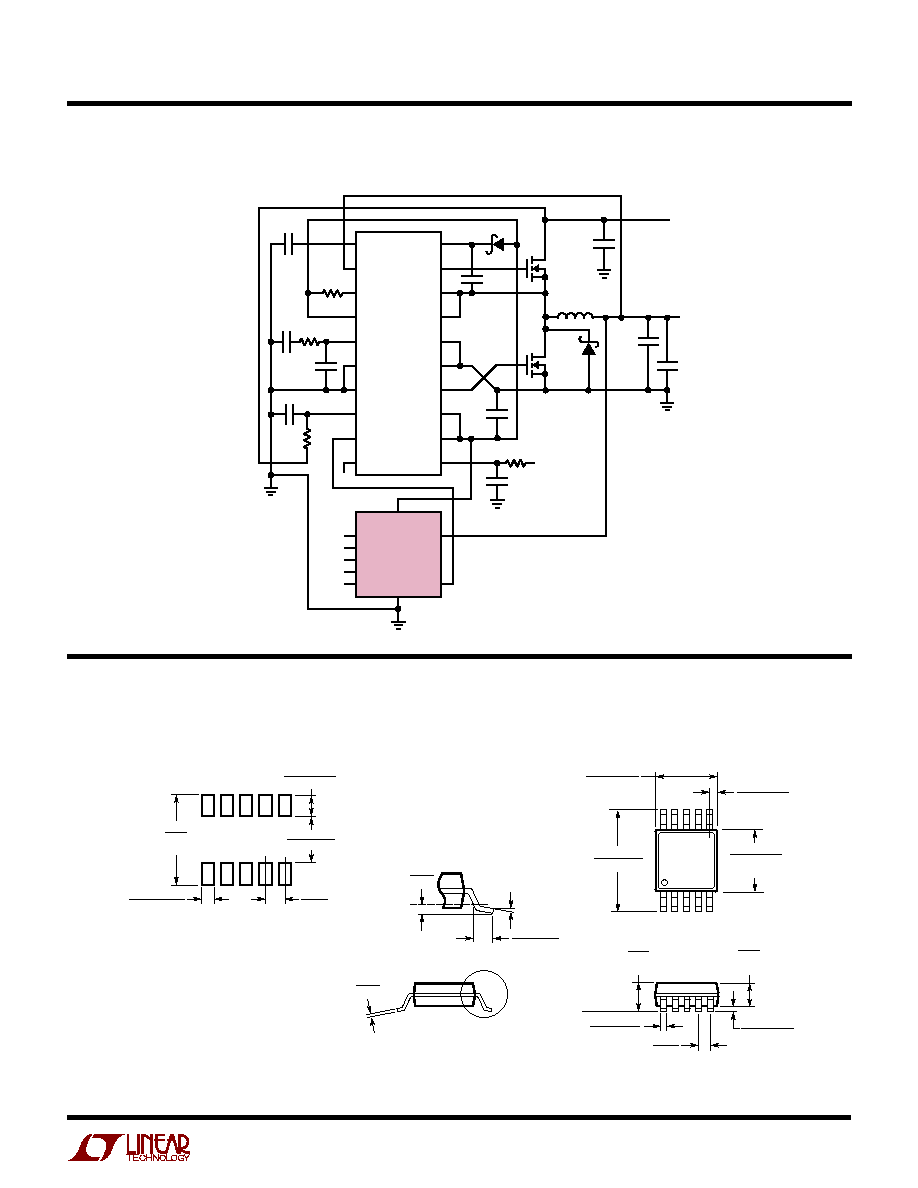
0.8V to 1.55V VID Programmable 15A Power Supply
RUN/SS
V
ON
PGOOD
V
RNG
I
TH
FCB
SGND
I
ON
V
FB
EXTV
CC
BOOST
TG
SW
SENSE
+
SENSE
≠
PGND
BG
DRV
CC
INTV
CC
V
IN
LTC3778
1
2
3
4
5
6
7
8
9
10
20
19
18
17
16
15
14
13
12
11
22pF
1500pF
20k
100k
330k
VID0
VID1
VID2
VID3
VID4
GND
SENSE
FB
V
CC
5V
FROM
µ
P
LTC1706-61
1
µ
F
X5R
0.01
µ
F
0.1
µ
F
0.22
µ
F
V
IN
V
IN
12V
V
OUT
0.8V TO 1.55V
15A
1
4.7
µ
F
X5R
6.3V
10
µ
F
16V
X5R
◊
4
IRF7811
IRF7811
B320A
0.68
µ
H
22
µ
F
6.3V
X5R
SP
270
µ
F
2V
◊
3
CMDSH-3
1706-61 TA02
1
2
3
4
7
9
10
5
6
U
TYPICAL APPLICATIO
Information furnished by Linear Technology Corporation is believed to be accurate and reliable.
However, no responsibility is assumed for its use. Linear Technology Corporation makes no represen-
tation that the interconnection of its circuits as described herein will not infringe on existing patent rights.
MSOP (MS) 0802
0.53
±
0.01
(.021
±
.006)
SEATING
PLANE
0.18
(.007)
1.10
(.043)
MAX
0.17 ≠ 0.27
(.007 ≠ .011)
TYP
0.13
±
0.076
(.005
±
.003)
0.86
(.034)
REF
0.50
(.0197)
BSC
1 2 3 4 5
4.90
±
0.15
(1.93
±
.006)
0.497
±
0.076
(.0196
±
.003)
REF
8
9
10
7 6
3.00
±
0.102
(.118
±
.004)
(NOTE 3)
3.00
±
0.102
(.118
±
.004)
NOTE 4
NOTE:
1. DIMENSIONS IN MILLIMETER/(INCH)
2. DRAWING NOT TO SCALE
3. DIMENSION DOES NOT INCLUDE MOLD FLASH, PROTRUSIONS OR GATE BURRS.
MOLD FLASH, PROTRUSIONS OR GATE BURRS SHALL NOT EXCEED 0.152mm (.006") PER SIDE
4. DIMENSION DOES NOT INCLUDE INTERLEAD FLASH OR PROTRUSIONS.
INTERLEAD FLASH OR PROTRUSIONS SHALL NOT EXCEED 0.152mm (.006") PER SIDE
5. LEAD COPLANARITY (BOTTOM OF LEADS AFTER FORMING) SHALL BE 0.102mm (.004") MAX
0.254
(.010)
0
∞
≠ 6
∞
TYP
DETAIL "A"
DETAIL "A"
GAUGE PLANE
5.23
(.206)
MIN
3.2 ≠ 3.45
(.126 ≠ .136)
0.889
±
0.127
(.035
±
.005)
RECOMMENDED SOLDER PAD LAYOUT
0.305
±
0.038
(.0120
±
.0015)
TYP
0.50
(.0197)
BSC
8
LTC1706-61
170661f
LT/TP 0603 1K ∑ PRINTED IN USA
©
LINEAR TECHNOLOGY CORPORATION 2002
Linear Technology Corporation
1630 McCarthy Blvd., Milpitas, CA 95035-7417
(408) 432-1900
q
FAX: (408) 434-0507
q
www.linear.com
RELATED PARTS
PART NUMBER
DESCRIPTION
COMMENTS
LTC1629-6
PolyPhase
Æ
Synchronous Step-Down Controller
Up to 12-Phase Operation, Up to 200A Power Supply
LTC3714
Single Phase Synchronous Step-Down Controller with VID
0.6V
V
OUT
1.75V, I
OUT
25A
LTC3716
2-Phase Synchronous Step-Down Controller with VID
0.6V
V
OUT
1.75V, I
OUT
40A
LTC3719
AMD Opteron CPU Power Supply
0.8V
V
OUT
1.55V, I
OUT
40A
LTC3731
3-Phase, 60A Synchronous Step-Down Controller
Single IC 60A Solution with Onboard MOSFET Drivers,
±
5% Output
Current Matching for Optimum Thermal Performance and Reliability
LTC3733
3-Phase, 60A Synchronous Step-Down Controller for
On-Board VID and MOSFET Drivers, 0.8V
V
OUT
1.55V, I
OUT
60A
AMD Opteron Processors
LTC3778
Optional R
SENSE
Synchronous Step-Down Controller
4V
V
IN
36V, 0.6V
V
OUT
(0.9)V
IN
, I
OUT
25A
PolyPhase is a registered trademark of Linear Technology Corporation.
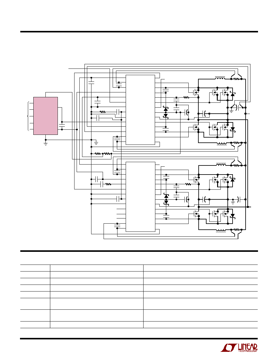
TYPICAL APPLICATIO
N
U
1706-61 TA04
RUN/SS
SENSE1
+
SENSE1
≠
EAIN
PLLFLTR
PLLIN
PHASMD
I
TH
SGND
V
DIFFOUT
V
OS
≠
V
OS
+
SENSE2
≠
SENSE2
+
RUN/SS
SENSE1
+
SENSE1
≠
EAIN
PLLFLTR
PLLIN
PHASMD
I
TH
SGND
V
DIFFOUT
V
OS
≠
V
OS
+
SENSE2
≠
SENSE2
+
CLKOUT
TG1
SW1
BOOST1
V
IN
BG1
EXTV
CC
INTV
CC
PGND
BG2
BOOST2
SW2
TG2
AMPMD
1
2
3
4
5
6
7
8
9
10
11
12
13
14
28
27
26
25
24
23
22
21
20
19
18
17
16
15
28
27
26
25
24
23
22
21
20
19
18
17
16
15
1
2
3
4
5
6
7
8
9
10
11
12
13
14
V
IN
12V
V
OUT
0.8V TO
1.55V
70A
VID0
VID1
VID2
VID3
VID4
1
2
3
4
7
V
CC
LTC1706-61
GND
9
5
10
6
M1 TO M12: FDS7760A
L1 TO L4: 1
µ
H SUMIDA CEPH149-IROMC
D7 TO D10: CENTROI CMDSH-3TR
C
OUT
: KEMET T510X477M006AS
f
SW
: 200kHz
FB
SENSE
FROM
µ
P
CLKOUT
TG1
SW1
BOOST1
V
IN
BG1
EXTV
CC
INTV
CC
PGND
BG2
BOOST2
SW2
TG2
AMPMD
10
M7
M10
M11
M8
M9
M6
M5
M4
M1
10
M2
M3
GND
150
µ
F, 16V
◊
2
GND
150
µ
F, 16V
◊
2
C
OUT
470
µ
F, 6.3V
◊
3
C
OUT
470
µ
F, 6.3V
◊
3
D3
MBRS
340T3
D2
MBRS
340T3
D1
MBRS
340T3
M12
L4
0.003
L1
L2
L3
0.003
0.003
0.003
D4
MBRS
340T3
0.47
µ
F
0.47
µ
F
5V
5V
LTC1629-6
LTC1629-6
0.47
µ
F
0.33
µ
F
0.33
µ
F
OPTIONAL SYNC
CLOCK IN
0.01
µ
F
47k
24k
10k
47pF
75k
6800pF
1000pF
1000pF
100pF
1000pF
1000pF
0.47
µ
F
1
µ
F
25V
1
µ
F
25V
22
µ
F
6.3V
22
µ
F
6.3V
1
µ
F
1
µ
F
+
+
+
+
+
+
D9
D10
D7
D8
47pF
V
DIFFOUT
V
OS
+
V
OS
≠
V
DIFFOUT
V
OS
+
V
OS
≠
100pF
VID Controlled High Current 70A 4-Phase Application