1
LTC1710
SMBus Dual Monolithic
High Side Switch
s
Two 0.4
/300mA N-Channel Switches
s
Available in MS8 and SO-8 Packages
s
SMBus and I
2
C Compatible
s
0.6V V
IL
and 1.4V V
IH
for DATA and CLK
s
Low Standby Current: 14
µ
A
s
Separate Drain Connection to SW0
s
Three Addresses from One Three-State Address Pin
s
Independent Control of Up to Six Switches
s
Built-In Power-On Reset Timer
s
Built-In Undervoltage Lockout
FEATURES
DESCRIPTIO
N
U
The LTC
Æ
1710 SMBus dual switch has two built-in 0.4
/
300mA switches that are controlled by a 2-wire SMBus
interface. With a low standby current of 14
µ
A (3.3V), the
LTC1710 operates over an input voltage range of 2.7V to
5.5V while maintaining the SMBus specified 0.6V V
IL
and
1.4V V
IH
input thresholds.
Using the 2-wire interface, CLK and DATA, the LTC1710
follows SMBus's Send Byte Protocol to independently
control the two 0.4
internal N-channel power switches,
which are fully enhanced by onboard charge pumps.
The LTC1710 has one three-state programmable
address pin that allows three different addresses for a total
of six available switches on the same bus. The LTC1710
also features a separate user-controlled drain supply
(SW0D) to Switch 0 so that it can be used to control
SMBus peripherials using a different power supply.
, LTC and LT are registered trademarks of Linear Technology Corporation.
APPLICATIO
N
S
U
s
Handheld Computer Power Management
s
Computer Peripheral Control
s
Laptop Computer Power Plane Switching
s
Portable Equipment Power Control
s
Industrial Control Systems
s
ACPI SMBus Interface
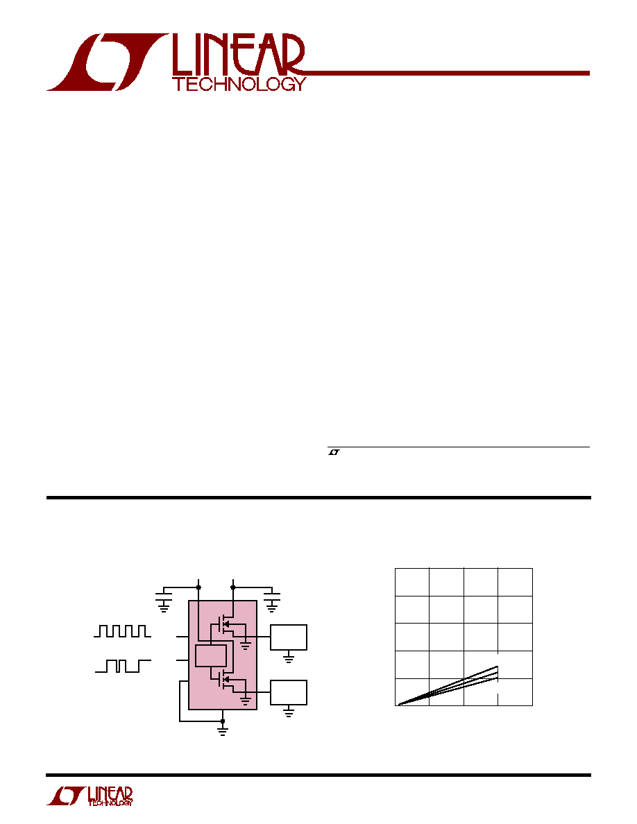
TYPICAL APPLICATIO
N
U
LOAD CURRENT (mA)
0
SWITCH VOLTAGE DROP (mV)
200
V
CC
= 3.3V
300
400
1710 TA02
100
0
100
200
300
500
T
A
= 25
∞
C
400
V
CC
= 2.7V
V
CC
= 5V
Switch Voltage Drop
vs Load Current
CHARGE
PUMP
8
1
2
10
µ
F
10
µ
F
7
5
CLOCK
DATA
6
FROM SMBus
3
AD1
(PROGRAMMABLE)
4
1710 TA01
V
CC
2.7V TO 5.5V
SW0D
0V TO V
CC
LTC1710
LOAD 1
SW0
SW1
LOAD 2
2
LTC1710
ABSOLUTE
M
AXI
M
U
M
RATINGS
W
W
W
U
(Voltages Referred to GND Pin) (Note 1)
Input Supply Voltage (V
CC
) .......................... ≠ 0.3V to 6V
Input Supply Voltage (V
CC
) with SW0 Connected
as a Low Side Switch ........................... ≠ 0.3V to 3.6V
DATA, CLK (Bus Pins 6, 5)......................... ≠ 0.3V to 6V*
AD1 ( Address Pin 3) ....................... ≠ 0.3V to V
CC
+ 0.3V
OUT0, OUT1 (Output Pins 2, 7) ................... ≠ 0.3V to 6V
SW0D (Switch 0 Drain Pin 1)....................... ≠ 0.3V to 6V
OUT0, OUT1 (Output Pins 2, 7)
Continuous .................................................... 300mA
Pulsed, < 10
µ
s (nonrepetitive) ............................... 1A
Operating Temperature Range
LTC1710C ................................................ 0
∞
C to 70
∞
C
LTC1710I ............................................ ≠ 40
∞
C to 85
∞
C
Junction Temperature** ...................................... 125
∞
C
Storage Temperature Range .................. ≠ 65
∞
C to 150
∞
C
Lead Temperature (Soldering, 10 sec)................... 300
∞
C
*Supply rails to DATA and CLK are independent of V
CC
to LTC1710.
**Although the LTC1710 can sustain T
JMAX
= 125
∞
C without damage, its internal protection
circuitry is set to shut down the switches at T
J
= 120
∞
C with 15
∞
C hysteresis.
ELECTRICAL CHARACTERISTICS
SYMBOL
PARAMETER
CONDITIONS
MIN
TYP
MAX
UNITS
V
CC
Operating Supply Voltage Range
q
2.7
5.5
V
I
VCC
Supply Current
Charge Pump Off, AD1 High or Low,
DATA and CLK High
V
CC
= 5V
q
17
30
µ
A
V
CC
= 3.3V
q
14
30
µ
A
V
CC
= 2.7V
q
11
30
µ
A
OUT0 or OUT1 High
(Command Byte XXXXXX01 or XXXXXX10)
q
200
300
µ
A
Both Outputs High (Command Byte XXXXXX11)
q
250
500
µ
A
R
DS(ON)
Power Switch On Resistance
V
CC
= 2.7V, I
OUT
= 300mA
0.55
V
CC
= 3.3V, I
OUT
= 300mA
0.46
0.7
V
CC
= 5V, I
OUT
= 300mA
0.40
0.6
V
UVLO
Undervoltage Lockout
Falling Edge (Note 2)
q
1.5
2.0
2.5
V
t
POR
Power-On Reset Delay Time
V
CC
= 2.7V (Note 3)
300
1000
µ
s
V
CC
= 5.5V
300
1000
µ
s
f
OSC
Charge Pump Oscillator Frequency
300
kHz
(Note 3)
T
A
= 25
∞
C, V
CC
= SW0D = 5V unless otherwise noted.
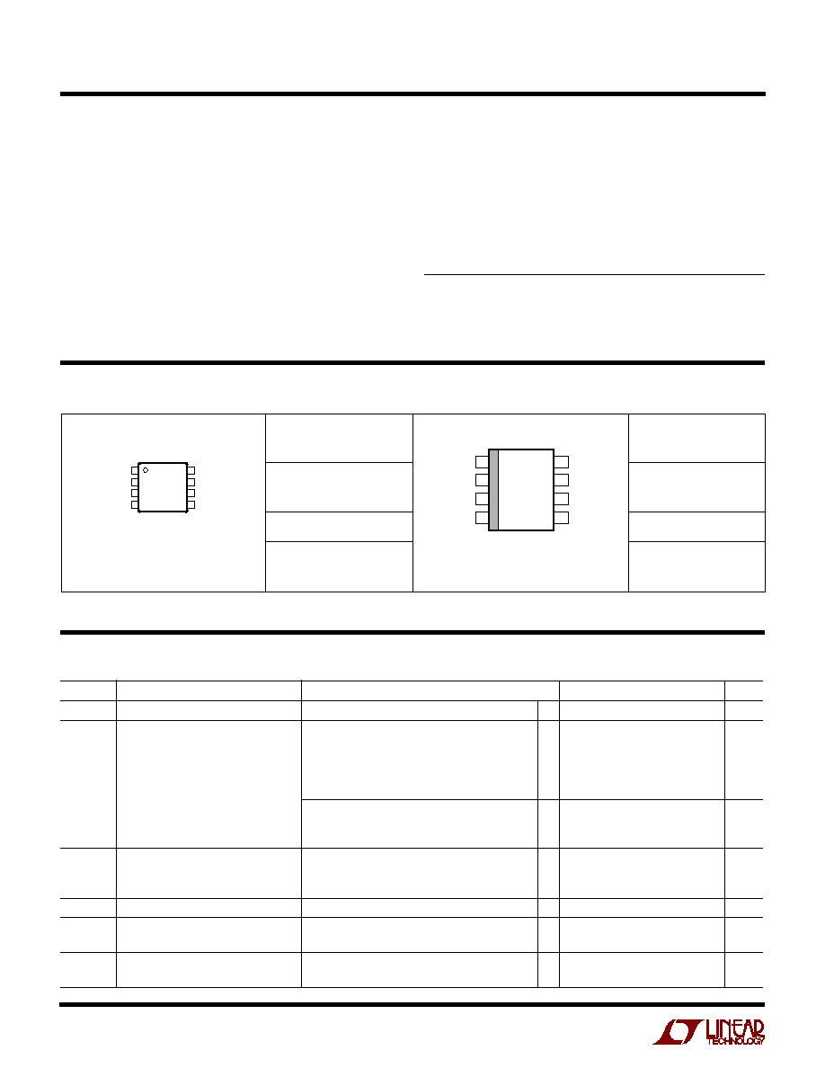
ORDER PART
NUMBER
S8 PART MARKING
PACKAGE/ORDER I
N
FOR
M
ATIO
N
W
U
U
Consult factory for Military grade parts.
ORDER PART
NUMBER
MS8 PART MARKING
LTDZ
T
JMAX
= 110
∞
C,
JA
= 110
∞
C/ W
1
2
3
4
8
7
6
5
TOP VIEW
V
CC
OUT1
DATA
CLK
SW0D
OUT0
AD1
GND
S8 PACKAGE
8-LEAD PLASTIC SO
1
2
3
4
SW0D
OUT0
AD1
GND
8
7
6
5
V
CC
OUT1
DATA
CLK
TOP VIEW
MS8 PACKAGE
8-LEAD PLASTIC MSOP
T
JMAX
= 110
∞
C,
JA
= 150
∞
C/ W
1710
1710I
LTC1710CS8
LTC1710IS8
LTC1710CMS8
3
LTC1710
ELECTRICAL CHARACTERISTICS
T
A
= 25
∞
C, V
CC
= SW0D = 5V unless otherwise noted.
SYMBOL
PARAMETER
CONDITIONS
MIN
TYP
MAX
UNITS
t
ON
Output Turn-On Time
V
CC
= 2.7V (From ON (Note 6) to V
OUT
= 90% V
CC
)
200
µ
s
(100
/1
µ
F Load)
V
CC
= 5.5V (From ON (Note 6) to V
OUT
= 90% V
CC
)
160
µ
s
t
OFF
Output Turn-Off Time
V
CC
= 2.7V (From OFF (Note 7) to V
OUT
= 10% V
CC
)
250
µ
s
(100
/1
µ
F Load)
V
CC
= 5.5V (From OFF (Note 7) to V
OUT
= 10% V
CC
)
250
µ
s
V
IL
DATA/CLK Input Low Voltage
V
CC
= 2.7V to 5.5V
q
0.6
V
AD1 Input Low Voltage
V
CC
= 2.7V to 5.5V
q
0.2
V
V
IH
DATA/CLK High Voltage
V
CC
= 2.7V to 5.5V
q
1.4
V
AD1 Input High Voltage
V
CC
= 2.7V to 5.5V
q
V
CC
≠ 0.2
V
V
OL
Data Output Low Voltage
V
CC
= 2.7V to 5.5V, I
PULL-UP
= 350
µ
A
q
0.18
0.4
V
C
IN
Input Capacitance (DATA, CLK, AD1)
5
pF
I
IN
Input Leakage Current (DATA, CLK)
q
±
1
µ
A
Input Leakage Current (AD1)
q
±
250
nA
SMBus Related Specifications (Note 5)
f
SMB
SMBus Operating Frequency
10
100
kHz
t
BUF
Bus Free Time Between
4.7
µ
s
Stop and Start
t
SU:STA
Start Condition Setup Time
4.7
µ
s
t
HD:STA
Start Condition Hold Time
4.0
µ
s
t
SU:STO
Stop Condition Setup Time
4.0
µ
s
t
HD: DAT
Data Hold Time
300
ns
t
SU:DAT
Data Setup Time
250
ns
t
LOW
Clock Low Period
4.7
µ
s
t
HIGH
Clock High Period
4.0
50
µ
s
t
f
Clock/Data Fall Time
300
ns
t
r
Clock/Data Rise Time
1000
ns
I
PULL-UP
Current Through External Pull-Up
V
CC
= 2.7V to 5.5V
100
350
µ
A
Resistor on DATA Pin
(Open-Drain Data Pull-Down Current Capacity)
The
q
denotes specifications which apply over the full operating
temperature range.
Note 1: Absolute Maximum Ratings are those values beyond which the life
of a device may be impaired.
Note 2: Approximately 3% hysteresis is provided to ensure stable operation
and eliminate false triggering by minor V
CC
glitches.
Note 3: Measured from V
CC
> V
UVLO
to SMBus ready for DATA input.
Note 4: The oscillator frequency is not tested directly but is inferred from
turn-on time.
Note 5: SMBus timing specifications are guaranteed but not tested.
Note 6: ON is enabled upon receiving the Stop condition from the SMBus
master.
Note 7: OFF is enabled upon receiving the Stop condition from the SMBus
master.
4
LTC1710
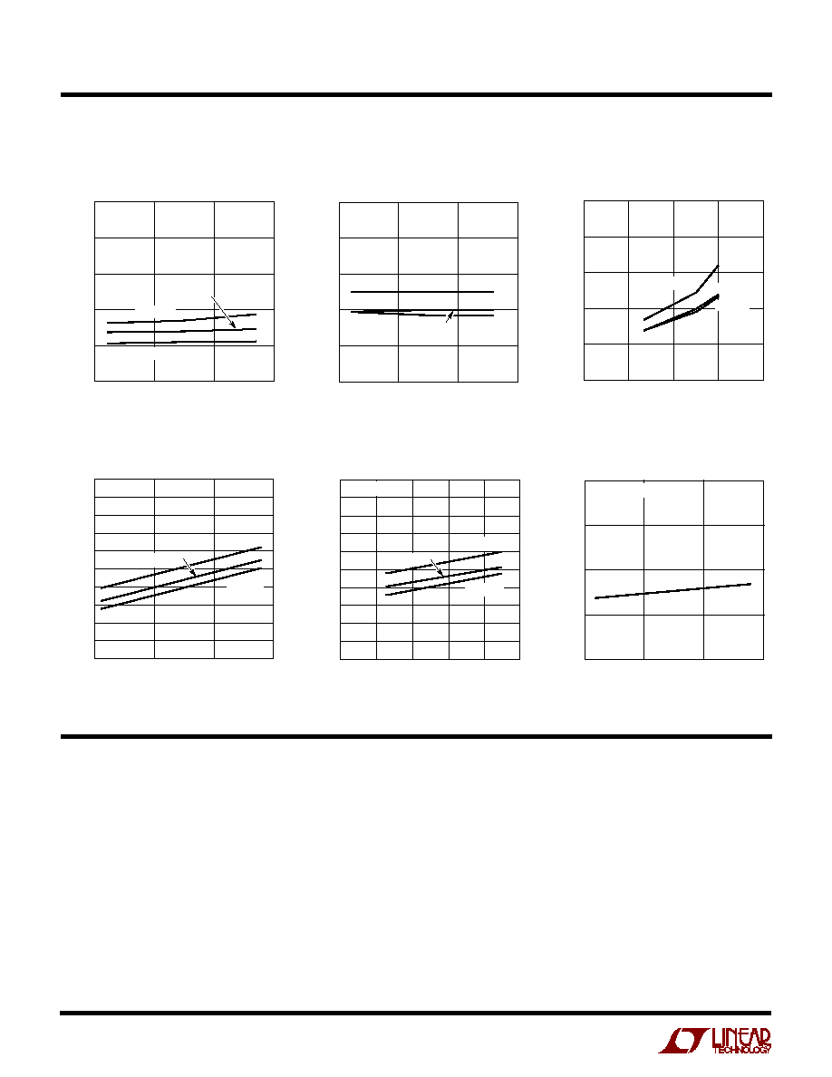
TYPICAL PERFOR A CE CHARACTERISTICS
U
W
TEMPERATURE (
∞
C)
≠ 50
STANDBY CURRENT (
µ
A)
10
100
1710 G01
0
0
50
20
30
40
50
V
CC
= 3.3V
V
CC
= 5V
V
CC
= 2.7V
Standby Current vs Temperature
Switch R
DS(ON)
vs Temperature
(SO-8 Package)
TEMPERATURE (
∞
C)
0
SWITCH R
DS(ON)
(
)
0.1
0.3
0.4
0.5
1.0
0.7
≠ 50
0
50
1710 G04
0.2
0.8
0.9
0.6
100
V
CC
= 2.7V
V
CC
= 3.3V
V
CC
= 5V
I
OUT
= 300mA
SUPPLY VOLTAGE (V)
0
0
SUPPLY CURRENT (
µ
A)
100
200
300
400
500
2
4
1710 G03
6
8
BOTH SW ON
SW1 ON
T
A
= 25
∞
C
SW0 ON
Supply Current (I
Q
)
vs Supply Voltage
TEMPERATURE (
∞
C)
DATA ACK V
OL
(mV)
200
300
100
1710 G06
100
0
≠ 50
0
50
400
I
PULL-UP
= 350
µ
A
TEMPERATURE (
∞
C)
≠ 50
SUPPLY CURRENT (
µ
A)
100
100
1710 G02
0
0
50
200
300
400
500
BOTH SW ON
SW1 ON
V
CC
= 5V
SW0 ON
Supply Current (I
Q
)
vs Temperature
Switch R
DS(ON)
vs Temperature
(MSOP Package)
TEMPERATURE (
∞
C)
0
SWITCH R
DS(ON)
(
)
0.6
0.8
1.0
80
1710 G05
0.4
0.2
0.5
0.7
0.9
0.3
0.1
0
20
40
60
100
V
CC
= 2.7V
V
CC
= 5V
V
CC
= 3.3V
I
OUT
= 300mA
Data ACK V
OL
vs Temperature
PI
N
FU
N
CTIO
N
S
U
U
U
SW0D (Pin 1): Drain Supply of Switch 0. User-program-
mable from 0V to V
CC
.
OUT0 (Pin 2): Source Output of Switch 0. Maximum load
of 300mA; controlled by LSB of command byte.
AD1 (Pin 3): Three-State Programmable Address Pin.
Must be connected directly to V
CC
, GND or V
CC
/2 (using
two resistors
1M). Do not float this pin.
GND (Pin 4): Ground Connection.
CLK (Pin 5): Serial Clock Interface. Must be pulled high to
V
CC
with external resistor. The pull-up current must be
limited to 350
µ
A.
DATA (Pin 6): Open-Drain Connected Serial Data Inter-
face. Must be pulled high to V
CC
with external resistor. The
pull-up current must be limited to 350
µ
A.
OUT1 (Pin 7): Source Output of Switch 1. Maximum load
of 300mA; controlled by 2nd LSB of command byte.
V
CC
(Pin 8): Input Supply Voltage. Operating range from
2.7V to 5.5V.
5
LTC1710
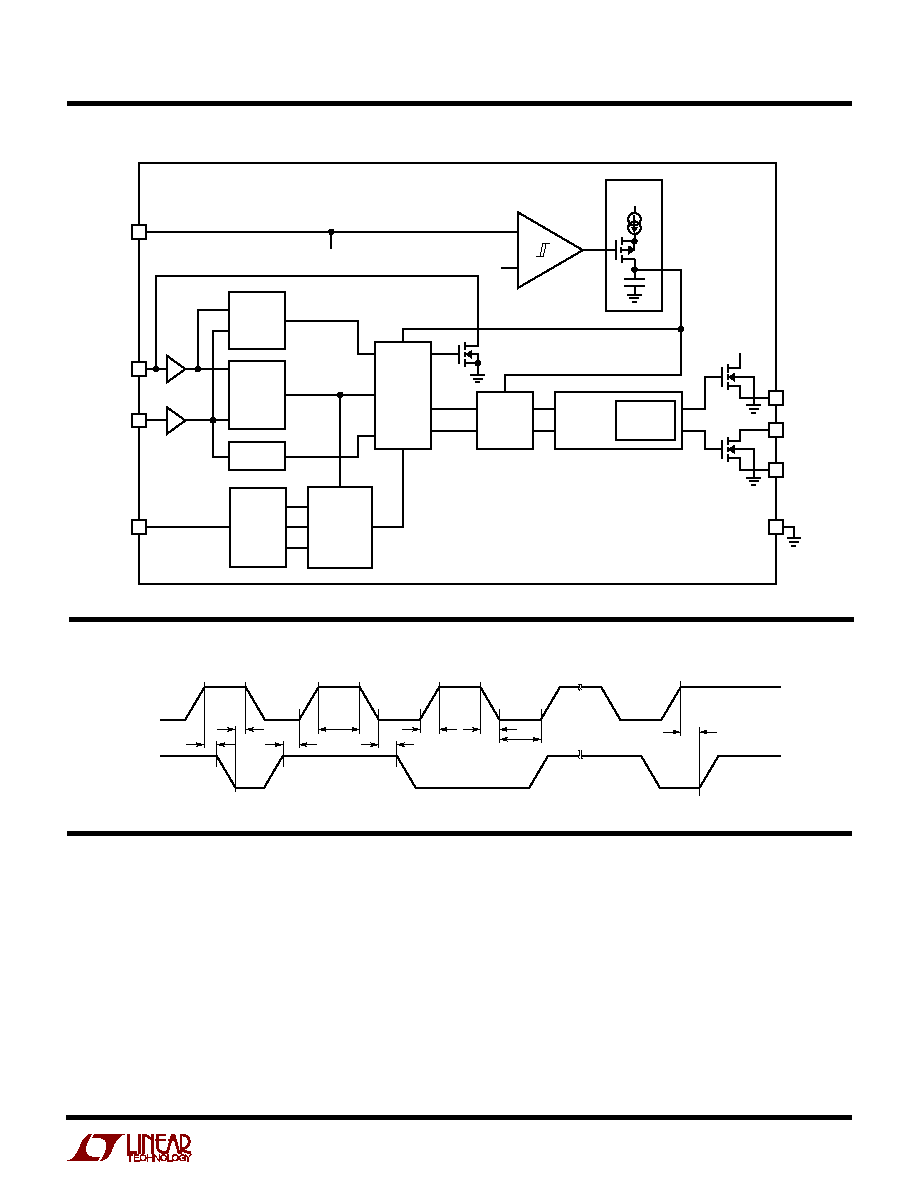
BLOCK DIAGRA
W
V
CC
V
CC
OUT1
7
1
2
SW0D
OUT0
4
GND
1710 BD
UNDERVOLTAGE
LOCKOUT
POWER-ON
RESET
2V
V
CC
ACK
A
B
OUTPUT
LATCHES
SHIFT
REGISTER
ADDRESS
DECODER
COUNTER
INPUT
BUFFERS
THERMAL
SHUTDOWN
REGULATED
CHARGE
PUMPS
ADDRESS
COMPARATOR
LOGIC
START
AND
STOP
DETECTORS
3
AD1
5
CLK
6
8
DATA
TI I G DIAGRA
U
W
W
CLK
DATA
START
STOP
1710 TD
t
SU:STO
t
LOW
t
HIGH
t
HD:DAT
t
SU:DAT
t
HD:STA
t
SU:STA
t
f
t
r
OPERATIO
U
SMBus Operation
SMBus is a serial bus interface that uses only two bus lines,
DATA and CLK, to control low power peripheral devices in
portable equipment. It consists of masters, also known as
hosts, and slave devices. The master of the SMBus is
always the one to initiate communications to the slave
devices by varying the status of the DATA and CLK lines.
The SMBus specification establishes a set of protocols that
devices on the bus must follow for communications.
The protocol that the LTC1710 uses is the Send Byte Pro-
tocol. In this protocol, the master first sends out a Start
signal by switching the DATA line from high to low while
CLK is high. (Because there may be more than one master
on the same bus, an arbitration process takes place if two
masters attempt to take control of the DATA line simulta-
neously; the first master that outputs a one while the other
master is zero loses the arbitration and becomes a slave
itself.) Upon detecting this Start signal, all slave devices on
the bus wake up and prepare to shift in the next byte of data.