Äîêóìåíòàöèÿ è îïèñàíèÿ www.docs.chipfind.ru
LTC1760
1
sn1760 1760is
Information furnished by Linear Technology Corporation is believed to be accurate and reliable.
However, no responsibility is assumed for its use. Linear Technology Corporation makes no represen-
tation that the interconnection of its circuits as described herein will not infringe on existing patent rights.
Final Electrical Specifications
s
SMBus Charger/Selector for Two Smart Batteries*
s
Voltage and Current Accuracy within 0.2% of Value
Reported by Battery
s
Simplifies Construction of "Smart Battery System
Manager"
s
Includes All SMBus Charger V1.1 Safety Features
s
Supports Autonomous Operation without a Host
s
SMBus Switching for Dual Batteries with Alarm
Monitoring for Charging Battery at All Times
s
Pin Programmable Limits for Maximum Charge
Current and Voltage Improve Safety
s
Allows Both Batteries to Discharge Simultaneously
into Single Load with Low Loss (Ideal Diode)
s
Fast Autonomous Power Path Switching (<10
µ
s)
s
Low Loss Simultaneous Charging of Two Batteries
s
>95% Efficient Synchronous Buck Charger
s
AC Adapter Current Limiting* Maximizes Charge Rate
s
SMBus Accelerator Improves SMBus Timing**
s
Available in 48-Lead TSSOP Package
APPLICATIO S
U
FEATURES
DESCRIPTIO
U
Dual Smart Battery
System Manager
May 2003
The LTC
®
1760 Smart Battery System Manager is a highly
integrated level 3 battery charger and selector intended for
products using dual smart batteries. Three SMBus inter-
faces allow the LTC1760 to servo to the internal voltage
and currents measured by the batteries while allowing an
SMBus Host to monitor either battery's status. Charging
accuracy is determined by the battery's internal voltage
and current measurement, typically better than
±
0.2%.
A proprietary PowerPath
TM
architecture supports simulta-
neous charging or discharging of both batteries. Typical
battery run times are extended by up to 10%, while
charging times are reduced by up to 50%. The LTC1760
automatically switches between power sources in less
than 10
µ
s to prevent power interruption upon battery or
wall adapter removal.
The LTC1760 implements all elements of a version 1.1
"Smart Battery System Manager" except for the genera-
tion of composite battery information. An internal multi-
plexer cleanly switches the SMBus Host to either of the
two attached Smart Batteries without generating partial
messages to batteries or SMBus Host. Thermistors on
both batteries are automatically monitored for tempera-
ture and disconnection information (SafetySignal).
, LTC and LT are registered trademarks of Linear Technology Corporation.
s
Portable Computers and Instruments
s
Standalone Dual Smart Battery Chargers
s
Battery Backup Systems
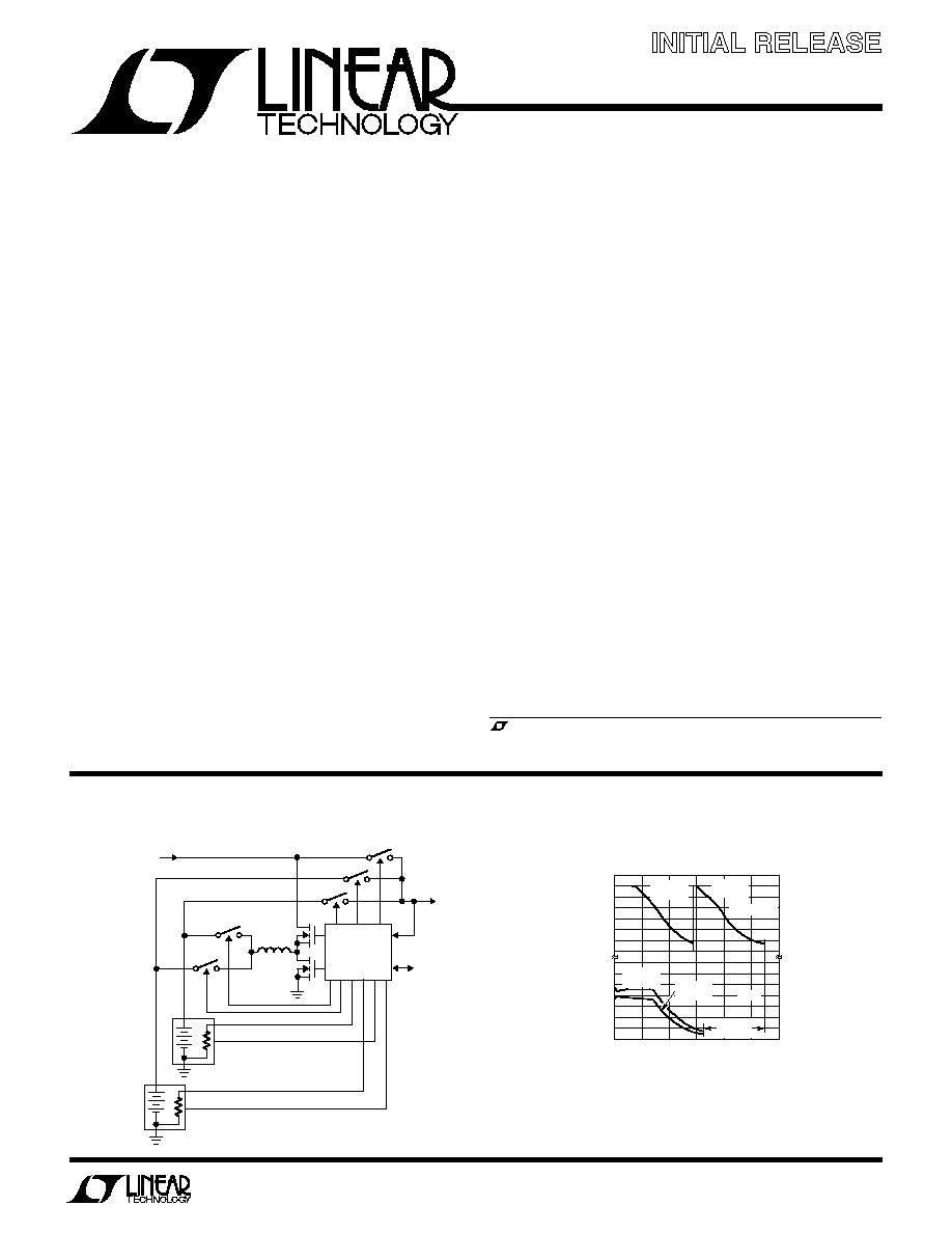
TYPICAL APPLICATIO
U
TIME (MINUTES)
BATTERY CURRENT (mA)
3500
3000
2500
2000
1500
1000
500
0
3500
3000
2500
2000
1500
1000
500
0
1760 TA03
0
50
100
150
200
250
300
BAT1
CURRENT
BAT2
CURRENT
SEQUENTIAL
DUAL
BAT1
CURRENT
100
MINUTES
BATTERY TYPE: 10.8V Li-Ion (MOLTECH NI2020)
REQUESTED CURRENT = 3A
REQUESTED VOLTAGE = 12.3V
MAX CHARGER CURRENT = 4.1A
BAT2
CURRENT
Dual Battery Charger/Selector System Architecture
Dual vs Sequential Charging
PowerPath is a trademark of Linear Technology Corporation
*U.S. Patent No. 5,723,970 **U.S. Patent No. 6,650,174
LTC1760
DC
IN
SYSTEM
POWER
SMBus (HOST)
1760 TA01
SafetySignal 1
SMBus 1
SafetySignal 2
SMBus 2
LTC1760
2
sn1760 1760is
Voltage from DCIN, SCP, SCN, CLP,
V
PLUS
, SW to GND ................................... 32V/0.3 V
Voltage from SCH1, SCH2 to GND ................ 28V/0.3 V
Voltage from BOOST to GND ........................ 37V/ 0.3V
CSP, CSN, BAT1, BAT2 to GND ..................... 28V/0.3V
LOPWR, DCDIV to GND ................................ 10V/ 0.3V
Voltage from V
CC2
, V
DDS
to GND .................... 7V/0.3 V
SDA1, SDA2, SDA, SCL1, SCL2, SCL, SMBALERT
to GND ........................................................ 7V/0.3V
MODE to GND ..................................... V
CC2
+0.3V/0.3V
COMP1 to GND ............................................... 5V/ 0.3V
Operating Ambient Temperature (Note 6) .... 0
°
C to 70
°
C
Operating Junction Temperature ...........40
°
C to 125
°
C
Storage Temperature .............................65
°
C to 150
°
C
Lead Temperature (Soldering, 10 sec).................. 300
°
C
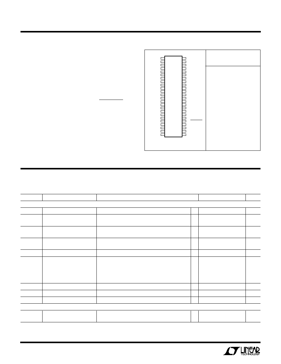
ORDER PART
NUMBER
T
JMAX
= 125
°
C,
JA
= 100
°
C/W
LTC1760CFW
ABSOLUTE AXI U
RATI GS
W
W
W
U
PACKAGE/ORDER I FOR ATIO
U
U
W
(Note 1)
ELECTRICAL CHARACTERISTICS
The
q
denotes the specifications which apply over the full operating
temperature range, otherwise specifications are at T
A
= 25
°
C. V
DCIN
= 20V, V
BAT1
= 12V, V
BAT2
= 12V, V
VDDS
= 3.3V, V
VCC2
= 5.2V
unless otherwise noted.
Consult LTC Marketing for parts specified with wider operating temperature ranges.
1
2
3
4
5
6
7
8
9
10
11
12
13
14
15
16
17
18
19
20
21
22
23
24
TOP VIEW
FW PACKAGE
48-LEAD PLASTIC TSSOP
48
47
46
45
44
43
42
41
40
39
38
37
36
35
34
33
32
31
30
29
28
27
26
25
SCH2
GCH2
GCH1
SCH1
TGATE
BOOST
SW
DCIN
V
CC
BGATE
PGND
COMP1
CLP
CSP
CSN
V
LIMIT
I
LIMIT
TH1B
TH1A
SMBALERT
TH2A
TH2B
MODE
V
CC2
V
PLUS
BAT2
BAT1
SCN
SCP
GDCO
GDCI
GB1O
GB1I
GB2O
GB2I
LOPWR
V
SET
I
TH
I
SET
DCDIV
SCL2
SCL
SCL1
V
DDS
SDA2
SDA
SDA1
GND
SYMBOL
PARAMETER
CONDITIONS
MIN
TYP
MAX
UNITS
Supply and Reference
DCIN Operating Range
DCIN Selected
6
28
V
I
CH0
DCIN Operating Current
Not Charging (DCIN Selected) (Note 10)
1
1.5
mA
I
CH1
Charging (DCIN Selected) (Note 10)
1.3
2
mA
I
VCC2_AC1
V
CC2
Operating Current
AC Present (Note 11)
0.75
1
mA
I
VCC2_AC0
AC Not Present (Note 11)
75
100
µ
A
Battery Operating Voltage Range Battery Selected, PowerPath Function
6
28
V
Battery Selected, Charging Function (Note 2)
0
28
V
I
BAT
Battery Drain Current
Battery Selected, Not Charging, V
DCIN
= 0V (Note 10)
175
µ
A
V
PLUS
Diodes Forward Voltage:
V
FDC
DCIN to V
PLUS
I
VCC
= 10mA
0.8
V
V
FB1
BAT1 to V
PLUS
I
VCC
= 0mA
0.7
V
V
FB2
BAT2 to V
PLUS
I
VCC
= 0mA
0.7
V
V
FSCN
SCN to V
PLUS
I
VCC
= 0mA
0.7
V
UVLO
Undervoltage Lockout Threshold V
PLUS
Ramping Down, Measured at V
PLUS
to GND
q
3
5
V
V
VCC
V
CC
Regulator Output Voltage
q
4.9
5.2
5.5
V
V
LDR
V
CC
Load Regulation
I
VCC
= 0mA to 10mA
q
0.2
1
%
Switching Regulator
V
TOL
Voltage Accuracy
With Respect to Voltage Reported by Battery
q
32
32
mV
V
CHMIN
< Requested Voltage < V
LIMIT
LTC1760
3
sn1760 1760is
ELECTRICAL CHARACTERISTICS
The
q
denotes the specifications which apply over the full operating
temperature range, otherwise specifications are at T
A
= 25
°
C. V
DCIN
= 20V, V
BAT1
= 12V, V
BAT2
= 12V, V
VDDS
= 3.3V, V
VCC2
= 5.2V
unless otherwise noted.
SYMBOL
PARAMETER
CONDITIONS
MIN
TYP
MAX
UNITS
I
TOL
Current Accuracy
With Respect to Current Reported by Battery
4mV/R
SENSE
< Requested Current < I
LIMIT
(Min)
(Note 12)
R
ILIMIT
= 0 (Short to GND)
q
2
2
mA
R
ILIMIT
= 10k
±
1%
q
4
4
mA
R
ILIMIT
= 33k
±
1%
q
8
8
mA
R
ILIMIT
= Open (or Short I
LIMIT
to V
CC2
)
q
8
8
mA
f
0SC
Regulator Switching Frequency
255
300
345
kHz
f
DO
Regulator Switching Frequency in Low
Duty Cycle
99%
20
25
kHz
Dropout Mode
DC
MAX
Regulator Maximum Duty Cycle
99
99.5
%
I
MAX
Maximum Current Sense Threshold
V
ITH
= 2.2V
140
155
190
mV
I
SNS
CA1 Input Bias Current
V
CSP
= V
CSN
> 5V
150
µ
A
CMSL
CA1/I
1
Input Common Mode Low
0
V
CMSH
CA1/I
1
Input Common Mode High
V
DCIN
0.2
V
V
CL1
CL1 Turn-On Threshold
95
100
105
mV
q
94
100
108
mV
TGATE Transition Time:
TG t
r
TGATE Rise Time
C
LOAD
= 3300pF, 10% to 90%
50
90
ns
TG t
f
TGATE Fall Time
C
LOAD
= 3300pF, 10% to 90%
50
90
ns
BGATE Transition Time:
BG t
r
BGATE Rise Time
C
LOAD
= 3300pF, 10% to 90%
50
90
ns
BG t
f
BGATE Fall Time
C
LOAD
= 3300pF, 10% to 90%
40
80
ns
Trip Points
V
TR
DCDIV/LOPWR Threshold
V
DCDIV
or V
LOPWR
Falling
q
1.166
1.19
1.215
V
V
THYS
DCDIV/LOPWR Hysteresis Voltage
V
DCDIV
or V
LOPWR
Rising
30
mV
I
BVT
DCDIV/LOPWR Input Bias Current
V
DCDIV
or V
LOPWR
= 1.19V
20
200
nA
V
TSC
Short-Circuit Comparator Threshold
V
SCP
V
SCN
, V
CC
5V
q
90
100
115
mV
V
FTO
Fast Power Path Turn-Off Threshold
V
DCDIV
Rising from V
CC
6
7
7.9
V
V
OVSD
Overvoltage Shutdown Threshold as a
V
SET
Rising from 0.8V until TGATE and BGATE
107
%
Percent of Programmed Charger Voltage
Stop Switching
DACs
I
RES
I
DAC
Resolution
Guaranteed Monotonic
10
Bits
I
DAC
Pulse Period:
t
IP
Normal Mode
6
10
15
µ
s
t
ILOW
Wake-Up Mode
50
ms
Charging Current Granularity
R
ILIMIT
= (Short I
LIMIT
to GND)
1
mA
R
ILIMIT
= 10k
±
1%
2
mA
R
ILIMIT
= 33k
±
1%
4
mA
R
ILIMIT
= Open (or Short I
LIMIT
to V
CC2
)
4
mA
I
WAKE_UP
Wake-Up Charging Current (Note 5)
60
80
100
mA
I
LIMIT
Charging Current Limit
R
ILIMIT
= 0 (Short I
LIMIT
to GND)
q
980
1000
1070
mA
R
ILIMIT
= 10k
±
1%
q
1960
2000
2140
mA
R
ILIMIT
= 33k
±
1%
q
2490
3000
3210
mA
R
ILIMIT
= Open (or Short I
LIMIT
to V
CC2
)
q
3920
4000
4280
mA
V
RES
V
DAC
Resolution
Guaranteed Monotonic (5V < V
BAT
< 25V)
11
Bits
LTC1760
4
sn1760 1760is
The
q
denotes the specifications which apply over the full operating
temperature range, otherwise specifications are at T
A
= 25
°
C. V
DCIN
= 20V, V
BAT1
= 12V, V
BAT2
= 12V, V
VDDS
= 3.3V, V
VCC2
= 5.2V
unless otherwise noted.
ELECTRICAL CHARACTERISTICS
V
STEP
V
DAC
Granularity
16
mV
V
LIMIT
Charging Voltage Limit
R
VLIMIT
= 0 (Short V
LIMIT
to GND)
q
8400
8432
8464
mV
(Note 7)
R
VLIMIT
= 10k
±
1%
q
12608
12640
12672
mV
R
VLIMIT
= 33k
±
1%
q
16832
16864
16896
mV
R
VLIMIT
= 100k
±
1%
q
21024
21056
21088
mV
R
VLIMIT
= Open (or Short V
LIMIT
to V
CC2
)(Note 13)
q
32768
mV
Charge Mux Switches
t
ONC
GCH1/GCH2 Turn-On Time
V
GCHX
V
SCHX
> 3V, C
LOAD
= 3000pF
5
10
ms
t
OFFC
GCH1/GCH2 Turn-Off Time
V
GCHX
V
SCHX
< 1V, from Time of
15
µ
s
V
CSN
< V
BATX
30mV, C
LOAD
= 3000pF
V
CON
CH Gate Clamp Voltage
I
LOAD
= 1
µ
A
GCH1
V
GCH1
V
SCH1
5
5.8
7
V
GCH2
V
GCH2
V
SCH2
5
5.8
7
V
V
COFF
CH Gate Off Voltage
I
LOAD
=10
µ
A
GCH1
V
GCH1
V
SCH1
0.8
0.4
0
V
GCH2
V
GCH2
V
SCH2
0.8
0.4
0
V
V
TOC
CH Switch Reverse Turn-Off Voltage
V
BATX
V
CSN
, 5V
V
BATX
28V
q
5
20
40
mV
V
FC
CH Switch Forward Regulation Voltage
V
CSN
V
BATX
,
5V
V
BATX
28V
q
15
35
60
mV
GCH1/GCH2 Active Regulation:
V
GCHX
V
SCHX
= 1.5V
I
OC(SRC)
Max Source Current
2
µ
A
I
OC(SNK)
Max Sink Current
2
µ
A
V
CHMIN
BATX Voltage Below Which
3.5
4.7
V
Charging is Inhibited (Does Not Apply
to Wake-Up Mode)
PowerPath Switches
t
DLY
Blanking Period after UVLO Trip
Switches Held Off
250
ms
t
PPB
Blanking Period after LOPWR Trip
Switches in 3-Diode Mode
1
sec
t
ONPO
GB1O/GB2O/GDCO Turn-On Time
V
GS
< 3V, from Time of Battery/DC
q
5
10
µ
s
Removal, or LOPWR Indication, C
LOAD
= 3000pF
t
OFFPO
GB1O/GB2O/GDCO Turn-Off Time
V
GS
> 1V, from Time of Battery/DC
q
3
7
µ
s
Removal, or LOPWR Indication, C
LOAD
= 3000pF
V
PONO
Output Gate Clamp Voltage
I
LOAD
= 1
µ
A
GB1O
Highest (V
BAT1
or V
SCP
) V
GB1O
4.75
6.25
7
V
GB2O
Highest (V
BAT2
or V
SCP
) V
GB2O
4.75
6.25
7
V
GDCO
Highest (V
DCIN
or V
SCP
) V
GDCO
4.75
6.25
7
V
V
POFFO
Output Gate Off Voltage
I
LOAD
= 25
µ
A
GB1O
Highest (V
BAT1
or V
SCP
) V
GB1O
0.18
0.25
V
GB2O
Highest (V
BAT2
or V
SCP
) V
GB2O
0.18
0.25
V
GDCO
Highest (V
DCIN
or V
SCP
) V
GDCO
0.18
0.25
V
V
TOP
PowerPath Switch Reverse
V
SCP
V
BATX
or V
SCP
V
DCIN
q
5
20
60
mV
Turn-Off Voltage
6V
V
SCP
28V
V
FP
PowerPath Switch Forward
V
BATX
V
SCP
or V
DCIN
V
SCP
q
0
25
50
mV
Regulation Voltage
6V
V
SCP
28V
GDCI/GB1I/GB2I Active Regulation:
(Note 3)
I
OP(SRC)
Source Current
4
µ
A
I
OP(SNK)
Sink Current
75
µ
A
SYMBOL
PARAMETER
CONDITIONS
MIN
TYP
MAX
UNITS
LTC1760
5
sn1760 1760is
ELECTRICAL CHARACTERISTICS
The
q
denotes the specifications which apply over the full operating
temperature range, otherwise specifications are at T
A
= 25
°
C. V
DCIN
= 20V, V
BAT1
= 12V, V
BAT2
= 12V, V
VDDS
= 3.3V, V
VCC2
= 5.2V
unless otherwise noted.
SYMBOL
PARAMETER
CONDITIONS
MIN
TYP
MAX
UNITS
t
ONPI
Gate B1I/B2I/DCI Turn-On Time
V
GS
< 3V, C
LOAD
= 3000pF (Note 4)
300
µ
s
t
OFFPI
Gate B1I/B2I/DCI Turn-Off Time
V
GS
> 1V, C
LOAD
= 3000pF (Note 4)
10
µ
s
V
PONI
Input Gate Clamp Voltage
I
LOAD
= 1
µ
A
GB1I
Highest (V
BAT1
or V
SCP
) V
GB1I
4.75
6.7
7.5
V
GB2I
Highest (V
BAT2
or V
SCP
) V
GB2I
4.75
6.7
7.5
V
GDCI
Highest (V
DCIN
or V
SCP
) V
GDCI
4.75
6.7
7.5
V
V
POFFI
Input Gate Off Voltage
I
LOAD
= 25
µ
A
GB1I
Highest (V
BAT1
or V
SCP
) V
GB1I
0.18
0.25
V
GB2I
Highest (V
BAT2
or V
SCP
) V
GB2I
0.18
0.25
V
GDCI
Highest (V
DCIN
or V
SCP
) V
GDCI
0.18
0.25
V
Thermistor
Thermistor Trip
C
LOAD(MAX)
= 300pF (Note 9)
q
95
100
105
k
(COLD-RANGE/OVER-RANGE)
R1A = R2A = 1130
±
1%
R1B = R2B = 54900
±
1%
Thermistor Trip
C
LOAD(MAX)
= 300pF (Note 9)
q
28.5
30
32.5
k
(IDEAL-RANGE /COLD-RANGE)
R1A = R2A = 1130
±
1%
R1B = R2B = 54900
±
1%
Thermistor Trip
C
LOAD(MAX)
= 300pF (Note 9)
q
2.85
3
3.15
k
(HOT-RANGE /IDEAL-RANGE)
R1A = R2A = 1130
±
1%
R1B = R2B = 54900
±
1%
Thermistor Trip
C
LOAD(MAX)
= 300pF (Note 9)
q
425
500
575
(UNDER-RANGE /HOT-RANGE)
R1A = R2A = 1130
±
1%
R1B = R2B = 54900
±
1%
Logic Levels
SCL/SCL1/SCL2/SDA/SDA1/
q
0.8
V
SDA2 Input Low Voltage (V
IL
)
SCL/SCL1/SCL2/SDA/SDA1/
q
2.1
V
SDA2 Input High Voltage (V
IH
)
SCL/SCL1/SCL2/SDA/SDA1/
V
SDA
, V
SCL
, V
SDA1
, V
SCL1
,
q
5
5
µ
A
SDA2 Input Leakage Current
V
SDA2
, V
SCL2
= 0.8V
SCL/SCL1/SCL2/SDA/SDA1/
V
SDA
, V
SCL
, V
SDA1
, V
SCL1
, V
SDA2
,
q
5
5
µ
A
SDA2 Input Leakage Current
V
SCL2
= 2.1V
I
PULLUP
SCL1/SDA1/SCL2/SDA2 Pull-Up
V
SCL1
= V
SDA1
= V
SCL2
= V
SDA2
= 0.4V
165
220
350
µ
A
Current When Not Connected to
V
VCC2
= 4.85V and 5.55V (Current is Through
SMBus Host.
Internal Series Resistor and Schottky to V
CC2
)
SCL1/SDA1/SCL2/SDA2
V
SDA1
, V
SCL1
, V
SDA2
, V
SCL2
= 0.8V
q
300
Series Impedance to Host SMBus.
SCL/SDA Output Low Voltage (V
OL
).
I
PULLUP
= 350
µ
A
q
0.4
V
LTC1760 Driving the Pin.
SCL1/SDA1/SCL2/SDA2 Pullup
I
PULLUP
Internal to LTC1760
q
0.4
V
Output Low Voltage (VOL).
LTC1760 Driving the Pin with Battery
SMBus not Connected to Host SMBus.
SCL1/SDA1/SCL2/SDA2
I
PULLUP
= 350
µ
A on Host Side
q
0.4
V
Output Low Voltage (V
OL
).
LTC1760 Driving the Pin with Battery
SMBus Connected to Host SMBus