18601lf Layout
1
LTC1860L/LTC1861L
18601Lf
APPLICATIO S
U
FEATURES
DESCRIPTIO
U
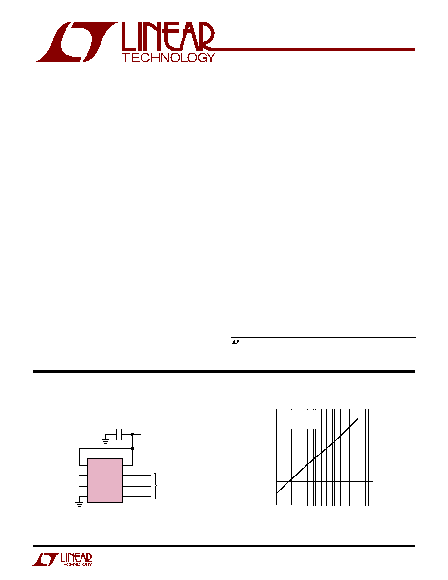
TYPICAL APPLICATIO
U
µ
Power, 3V, 12-Bit, 150ksps
1- and 2-Channel ADCs in MSOP
Single 3V Supply, 150ksps, 12-Bit Sampling ADC
Supply Current vs Sampling Frequency
The LTC
®
1860L/LTC1861L are 12-bit A/D converters that
are offered in MSOP and SO-8 packages and operate on a
single 3V supply. At 150ksps, the supply current is only
450
µ
A. The supply current drops at lower speeds because
the LTC1860L/LTC1861L automatically power down be-
tween conversions. These 12-bit switched capacitor suc-
cessive approximation ADCs include sample-and-holds.
The LTC1860L has a differential analog input with an
external reference pin. The LTC1861L offers a software-
selectable 2-channel MUX and an external reference pin on
the MSOP version.
The 3-wire, serial I/O, MSOP or SO-8 package and
extremely high sample rate-to-power ratio make these
ADCs ideal choices for compact, low power, high speed
systems.
These ADCs can be used in ratiometric applications or with
external references. The high impedance analog inputs
and the ability to operate with reduced spans down to 1V
full scale allow direct connection to signal sources in many
applications, eliminating the need for external gain stages.
s
12-Bit 150ksps ADCs in MSOP Package
s
Single 3V Supply
s
Low Supply Current: 450
µ
A (Typ)
s
Auto Shutdown Reduces Supply Current
to 10
µ
A at 1ksps
s
True Differential Inputs
s
1-Channel (LTC1860L) or 2-Channel (LTC1861L)
Versions
s
SPI/MICROWIRE
TM
Compatible Serial I/O
s
High Speed Upgrade to LTC1285/LTC1288
s
Pin Compatible with 16-Bit LTC1864L/LTC1865L
s
No Minimum Data Transfer Rate
, LTC and LT are registered trademarks of Linear Technology Corporation.
s
High Speed Data Acquisition
s
Portable or Compact Instrumentation
s
Low Power Battery-Operated Instrumentation
s
Isolated and/or Remote Data Acquisition
MICROWIRE is a trademark of National Semiconductor Corporation.
1
2
3
4
8
7
6
5
V
REF
IN
+
IN
GND
V
CC
SCK
SDO
CONV
LTC1860L
1860L TA01
ANALOG INPUT
0V TO 3V
3V
1
µ
F
SERIAL DATA LINK TO
ASIC, PLD, MPU, DSP
OR SHIFT REGISTERS
SAMPLING FREQUENCY (kHz)
0.1
SUPPLY CURRENT (
µ
A)
1
10
100
1000
0.01
1
10
1000
1860L/61L TA02
0.1
100
CONV LOW = 1.5
µ
s
T
A
= 25
°
C
V
CC
= 2.7V
2
LTC1860L/LTC1861L
18601Lf
PARAMETER
CONDITIONS
MIN
TYP
MAX
UNITS
Resolution
q
12
Bits
No Missing Codes Resolution
q
12
Bits
INL
(Note 3)
q
±
1
LSB
Transition Noise
0.13
LSB
RMS
Gain Error
q
±
20
mV
Offset Error
q
±
2
±
5
mV
Input Differential Voltage Range
V
IN
= IN
+
IN
q
0
V
REF
V
Absolute Input Range
IN
+
Input
0.05
V
CC
+ 0.05
V
IN
Input
0.05
V
CC
/2
V
V
REF
Input Range
LTC1860L S0-8 and MSOP, LTC1861L MSOP
1
V
CC
V
Analog Input Leakage Current
(Note 4)
q
±
1
µ
A
C
IN
Input Capacitance
In Sample Mode
12
pF
During Conversion
5
pF
Power Dissipation .............................................. 400mW
Operating Temperature Range
LTC1860LC/LTC1861LC ......................... 0
°
C to 70
°
C
LTC1860LI/LTC1861LI ...................... 40
°
C to 85
°
C
Storage Temperature Range ................. 65
°
C to 150
°
C
Lead Temperature (Soldering, 10 sec)................. 300
°
C
Supply Voltage (V
CC
) ................................................. 7V
Ground Voltage Difference
AGND, DGND LTC1861L MSOP Package .........
±
0.3V
Analog Input .................... (GND 0.3V) to (V
CC
+ 0.3V)
Digital Input ..................................... (GND 0.3V) to 7V
Digital Output .................. (GND 0.3V) to (V
CC
+ 0.3V)
(Notes 1, 2)
ORDER PART
NUMBER
MS8 PART MARKING
ORDER PART
NUMBER
LTC1860LCMS8
LTC1860LIMS8
LTD2
LTD3
MS PART MARKING
T
JMAX
= 150
°
C,
JA
= 210
°
C/W
T
JMAX
= 150
°
C,
JA
= 175
°
C/W
1
2
3
4
V
REF
IN
+
IN¯
GND
8
7
6
5
V
CC
SCK
SDO
CONV
TOP VIEW
MS8 PACKAGE
8-LEAD PLASTIC MSOP
ABSOLUTE AXI U RATI GS
W
W
W
U
PACKAGE/ORDER I FOR ATIO
U
U
W
LTC1861LCMS
LTC1861LIMS
LTD4
LTD5
Consult LTC Marketing for parts specified with wider operating temperature ranges.
The
q
denotes specifications which apply over the full operating temperature range, otherwise specifications are T
A
= 25
°
C.
V
CC
= 2.7V, V
REF
= 2.5V, f
SCK
= f
SCK(MAX)
as defined in Recommended Operating Conditions, unless otherwise noted.
CO VERTER A D ULTIPLEXER CHARACTERISTICS
U
W
U
ORDER PART
NUMBER
S8 PART MARKING
LTC1860LCS8
LTC1860LIS8
1860L
1860LI
1
2
3
4
8
7
6
5
TOP VIEW
S8 PACKAGE
8-LEAD PLASTIC SO
V
REF
IN
+
IN
GND
V
CC
SCK
SDO
CONV
ORDER PART
NUMBER
S8 PART MARKING
LTC1861LCS8
LTC1861LIS8
1861L
1861LI
T
JMAX
= 150
°
C,
JA
= 210
°
C/W
T
JMAX
= 150
°
C,
JA
= 175
°
C/W
1
2
3
4
5
CONV
CH0
CH1
AGND
DGND
10
9
8
7
6
V
REF
V
CC
SCK
SDO
SDI
TOP VIEW
MS PACKAGE
10-LEAD PLASTIC MSOP
1
2
3
4
8
7
6
5
TOP VIEW
S8 PACKAGE
8-LEAD PLASTIC SO
CONV
CH0
CH1
GND
V
CC
SCK
SDO
SDI
3
LTC1860L/LTC1861L
18601Lf
The
q
denotes specifications which apply
over the full operating temperature range, otherwise specifications are T
A
= 25
°
C. V
CC
= 2.7V, V
REF
= 2.5V, unless otherwise noted.
T
A
= 25
°
C. V
CC
= 3V, V
REF
= 3V, f
SAMPLE
= 150kHz, unless otherwise specified.
SYMBOL
PARAMETER
CONDITIONS
MIN
TYP
MAX
UNITS
SNR
Signal-to-Noise Ratio
72
dB
S/(N + D) Signal-to-Noise Plus Distortion Ratio
1kHz Input Signal
72
dB
THD
Total Hamonic Distortion Up to 5th Harmonic 1kHz Input Signal
86
dB
Full Power Bandwidth
10
MHz
Full Linear Bandwidth
S/(N + D)
68dB
30
kHz
DY
A
IC ACCURACY
U
W
DIGITAL A D DC ELECTRICAL CHARACTERISTICS
U
The
q
denotes specifications which apply over the
full operating temperature range, otherwise specifications are T
A
= 25
°
C.
RECO
E
DED OPERATI
G CO DITIO
S
U
U
U
U
W
W
SYMBOL
PARAMETER
CONDITIONS
MIN
TYP
MAX
UNITS
V
IH
High Level Input Voltage
V
CC
= 3.3V
q
1.9
V
V
IL
Low Level Input Voltage
V
CC
= 2.7V
q
0.45
V
I
IH
High Level Input Current
V
IN
= V
CC
q
2.5
µ
A
I
IL
Low Level Input Current
V
IN
= 0V
q
2.5
µ
A
V
OH
High Level Output Voltage
V
CC
= 2.7V, I
O
= 10
µ
A
q
2.3
2.6
V
V
CC
= 2.7V, I
O
= 360
µ
A
q
2.1
2.45
V
V
OL
Low Level Output Voltage
V
CC
= 2.7V, I
O
= 400
µ
A
q
0.3
V
I
OZ
Hi-Z Output Leakage
CONV = V
CC
q
±
3
µ
A
I
SOURCE
Output Source Current
V
OUT
= 0V
6.5
mA
I
SINK
Output Sink Current
V
OUT
= V
CC
6.5
mA
I
REF
Reference Current (LTC1860L SO-8, MSOP
CONV = V
CC
q
0.001
3
µ
A
and LTC1861L MSOP)
f
SMPL
= f
SMPL(MAX)
q
0.01
0.1
mA
I
CC
Supply Current
CONV = V
CC
After Conversion
q
0.5
10
µ
A
f
SMPL
= f
SMPL(MAX)
q
0.45
1.0
mA
P
D
Power Dissipation
f
SMPL
= f
SMPL(MAX)
1.22
mW
SYMBOL
PARAMETER
CONDITIONS
MIN
TYP
MAX
UNITS
V
CC
Supply Voltage
2.7
3.6
V
f
SCK
Clock Frequency
q
DC
8
MHz
t
CYC
Total Cycle Time
12 · SCK + t
CONV
µ
s
t
SMPL
Analog Input Sampling Time (Note 5)
LTC1860L
12
SCK
LTC1861L
10
SCK
t
suCONV
Setup Time CONV
Before First SCK
,
60
ns
(See Figure 1)
t
hDI
Holdtime SDI After SCK
LTC1861L
30
ns
t
suDI
Setup Time SDI Stable Before SCK
LTC1861L
30
ns
t
WHCLK
SCK High Time
f
SCK
= f
SCK(MAX)
45%
1/f
SCK
t
WLCLK
SCK Low Time
f
SCK
= f
SCK(MAX)
45%
1/f
SCK
t
WHCONV
CONV High Time Between Data
t
CONV
µ
s
Transfer Cycles
t
WLCONV
CONV Low Time During Data Transfer
12
SCK
t
hCONV
Hold Time CONV Low After Last SCK
26
ns
4
LTC1860L/LTC1861L
18601Lf
SYMBOL
PARAMETER
CONDITIONS
MIN
TYP
MAX
UNITS
t
CONV
Conversion Time (See Figure 1)
q
3.7
4.66
µ
s
f
SMPL(MAX)
Maximum Sampling Frequency
q
150
kHz
t
dDO
Delay Time, SCK
to SDO Data Valid
C
LOAD
= 20pF
45
55
ns
q
60
ns
t
dis
Delay Time, CONV
to SDO Hi-Z
q
55
120
ns
t
en
Delay Time, CONV
to SDO Enabled
C
LOAD
= 20pF
q
35
120
ns
t
hDO
Time Output Data Remains
C
LOAD
= 20pF
q
5
15
ns
Valid After SCK
t
r
SDO Rise Time
C
LOAD
= 20pF
25
ns
t
f
SDO Fall Time
C
LOAD
= 20pF
12
ns
The
q
denotes specifications which apply over the full operating temperature
range, otherwise specifications are T
A
= 25
°
C. V
CC
= 2.7V, V
REF
= 2.5V, f
SCK
= f
SCK(MAX)
as defined in Recommended Operating
Conditions, unless otherwise noted.
TI I G CHARACTERISTICS
U
W
TYPICAL PERFOR A CE CHARACTERISTICS
U
W
Supply Current vs Sampling
Frequency
Supply Current vs Temperature
Sleep Current vs Temperature
SAMPLING FREQUENCY (kHz)
0.1
SUPPLY CURRENT (
µ
A)
1
10
100
1000
0.01
1
10
1000
1860L/61L G01
0.1
100
TEMPERATURE (
°
C)
50
SUPPLY CURRENT (
µ
A)
600
500
400
300
200
100
0
25
75
1860L/61L G02
25
0
50
100
125
TEMPERATURE (
°
C)
50
SHUTDOWN CURRENT (
µ
A)
20
15
10
5
0
25
75
1860L/61L G03
25
0
50
100
125
f
S
= 150kHz
V
CC
= 2.7V
V
REF
= 2.5V
CONV LOW = 1.5
µ
s
T
A
= 25
°
C
V
CC
= 2.7V
f
S
= 150kHz
V
CC
= 2.7V
V
REF
= 2.5V
Note 1: Absolute Maximum Ratings are those values beyond which the life
of a device may be impaired.
Note 2: All voltage values are with respect to GND.
Note 3: Integral nonlinearity is defined as deviation of a code from a
straight line passing through the actual endpoints of the transfer curve.
The deviation is measured from the center of the quantization band.
Note 4: Channel leakage current is measured while the part is in sample
mode.
Note 5: Assumes f
SCK
= f
SCK(MAX)
. In the case of the LTC1860L SCK does
not have to be clocked during this time if the SDO data word is not
desired. In the case of the LTC1861L a minimum of 2 clocks are required
on the SCK input after CONV falls to configure the MUX during this time.
5
LTC1860L/LTC1861L
18601Lf
Reference Current vs
Sampling Rate
Reference Current vs
Temperature
Reference Current vs
Reference Voltage
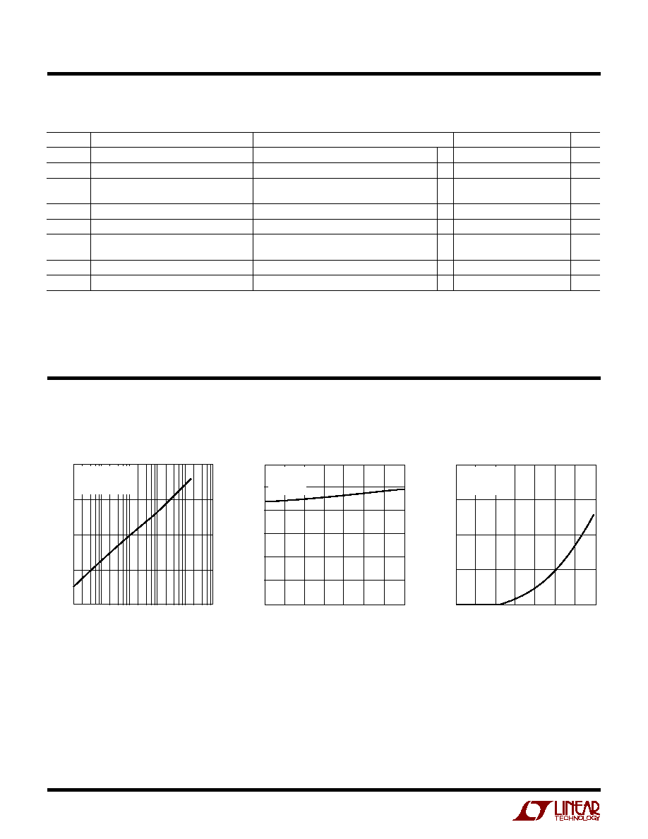
Typical INL Curve
Typical DNL Curve
Analog Input Leakage vs
Temperature
TYPICAL PERFOR A CE CHARACTERISTICS
U
W
Change in Offset vs
Reference Voltage
Change in Offset vs Temperature
Change in Gain Error vs
Reference Voltage
TEMPERATURE (
°
C)
50
REFERENCE CURRENT (
µ
A)
25
20
15
10
5
0
25
75
1860L/61L G05
25
0
50
100
125
f
S
= 150kHz
V
CC
= 2.7V
V
REF
= 2.5V
TEMPERATURE (
°
C)
50
ANALOG INPUT LEAKAGE (nA)
100
75
50
25
0
25
75
1860L/61L G09
25
0
50
100
125
CONV = 0V
V
CC
= 2.7V
V
REF
= 2.5V
SAMPLING FREQUENCY (kHz)
0
REFERENCE CURRENT (
µ
A)
25
50
75
100
1860L/61L G04
125
10
9
8
7
6
5
4
3
2
1
0
150
CONV LOW = 1.5
µ
s
T
A
= 25
°
C
V
CC
= 2.7V
V
REF
= 2.5V
CODE
0
INL ERROR (LSBs)
4096
1860L/61L G07
1024
2048
3072
1.0
0.5
0
0.5
1.0
512
1536
2560
3584
f
S
= 150kHz
T
A
= 25
°
C
V
CC
= 2.7V
V
REF
= 2.5V
CODE
0
DNL ERROR (LSBs)
4096
1860L/61L G08
1024
2048
3072
1.0
0.5
0
0.5
1.0
512
1536
2560
3584
f
S
= 150kHz
T
A
= 25
°
C
V
CC
= 2.7V
V
REF
= 2.5V
REFERENCE VOLTAGE (V)
0
CHANGE IN OFFSET (LSB)
4
1860L/61L G10
1
2
3
2
1
0
1
2
f
S
= 150kHz
T
A
= 25
°
C
V
CC
= 3.6V
REFERENCE VOLTAGE (V)
0
GHANGE IN GAIN ERROR (LSB)
4
1860L/61L G12
1
2
3
2
1
0
1
2
f
S
= 150kHz
T
A
= 25
°
C
V
CC
= 3.6V
TEMPERATURE (
°
C)
50
25
75
1860L/61L G11
25
0
50
100
125
CHANGE IN OFFSET (LSB)
1.0
0.8
0.6
0.4
0.2
0
0.2
0.4
0.6
0.8
1.0
f
S
= 150kHz
V
CC
= 2.7V
V
REF
= 2.5V
REFERENCE VOLTAGE (V)
0
REFERENCE CURRENT (
µ
A)
0.5
1.0
2.0
1.5
3.0
2.5
1860L/61L G06
3.5
25
20
15
10
5
0
4.0
f
S
= 150kHz
T
A
= 25
°
C
V
CC
= 3.6V