 | ÐлекÑÑоннÑй компоненÑ: LTC1875 | СкаÑаÑÑ:  PDF PDF  ZIP ZIP |
Äîêóìåíòàöèÿ è îïèñàíèÿ www.docs.chipfind.ru
1
LTC1875
1875f
15
µ
A Quiescent Current
1.5A Monolithic Synchronous
Step-Down Regulator
s
Portable Computers
s
Portable Instruments
s
Wireless Modems
, LTC and LT are registered trademarks of Linear Technology Corporation.
High Efficiency Step-Down Converter
s
High Efficiency: Up to 95%
s
Low Quiescent Current: Only 15
µ
A with No Load
s
550kHz Constant Frequency Operation
s
2.65V to 6V Input Voltage Range
s
V
OUT
from 0.8V to V
IN
, I
OUT
to 1.5A
s
True PLL Frequency Locking from 350kHz to 750kHz
s
Power Good Output Voltage Monitor
s
Low Dropout Operation: 100% Duty Cycle
s
Burst Mode
®
or Pulse Skipping Operation
s
Current Mode Operation for Excellent Line and Load
Transient Response
s
Shutdown Mode Draws < 1
µ
A Supply Current
s
±
2% Output Voltage Accuracy
s
Overcurrent and Overtemperature Protected
s
Available in 16-Lead SSOP Package
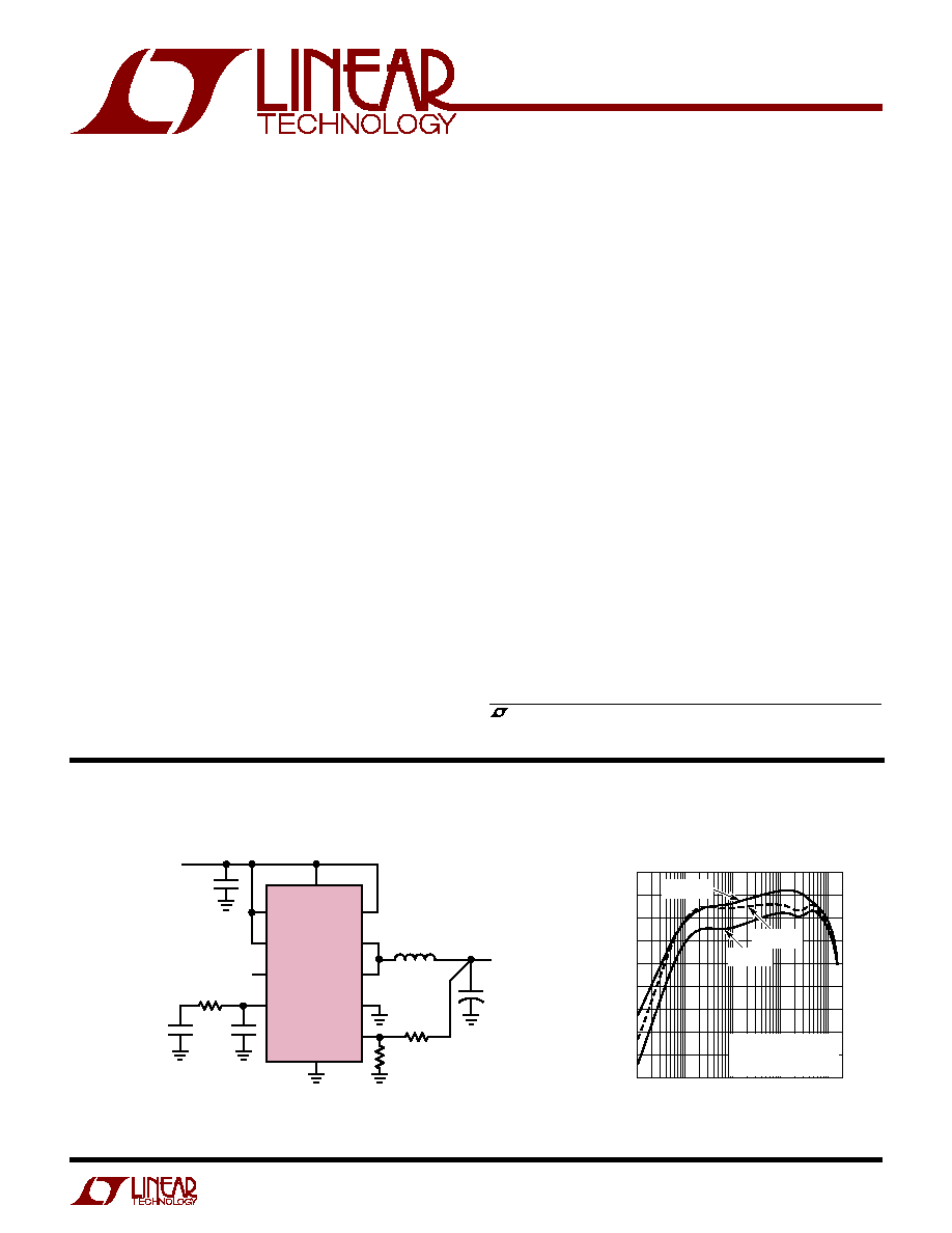
The LTC
®
1875 is a high efficiency 1.5A monolithic syn-
chronous buck regulator using a constant frequency,
current mode architecture. Operating supply current is
only 15
µ
A with no load and drops to < 1
µ
A in shutdown.
The input supply voltage range of 2.65V to 6V makes the
LTC1875 ideally suited for single Li-Ion battery-powered
applications. 100% duty cycle provides low dropout op-
eration, extending battery life in portable systems.
The switching frequency is internally set to 550kHz, allow-
ing the use of small surface mount inductors and capaci-
tors. For noise sensitive applications, the LTC1875 can be
externally synchronized from 350kHz to 750kHz. Burst
Mode operation is inhibited during synchronization or
when the SYNC/MODE pin is pulled low.
The internal synchronous switch increases efficiency and
eliminates the need for an external Schottky diode. Low
output voltages are easily supported with a 0.8V feedback
reference voltage. The LTC1875 is available in a 16-lead
SSOP package.
Burst Mode is a registered trademark of Linear Technology Corporation.
RUN/SS
SYNC/MODE
PGOOD
I
TH
PV
IN
SWP
SWN
PGND
V
FB
SV
IN
LTC1875
28.0k
C
IN
: TAIYO YUDEN CERAMIC JMK325BJ226MM
C
OUT
: SANYO POSCAP 6TPA47M
L1: TOKO 646CY-6R8M
*V
OUT
CONNECTED TO V
IN
(MINUS SWITCH AND L1 VOLTAGE DROP) FOR 2.65V < V
IN
< 3.3V
1875 TA01
220pF
150k
88.7k
C
OUT
47
µ
F
V
OUT
*
3.3V
L1
6.8
µ
H
SGND
47pF
C
IN
22
µ
F
V
IN
2.65V TO 6V
+
Efficiency vs Output Load Current
OUPUT CURRENT (mA)
EFFICIENCY (%)
100
95
90
85
80
75
70
65
60
55
0.1
10
100
1875 TA01a
1
1000
Burst Mode OPERATION
V
OUT
= 3.3V
L = 6.8
µ
H
V
IN
= 4.2V
V
IN
= 6V
V
IN
= 3.6V
FEATURES
DESCRIPTIO
U
APPLICATIO S
U
TYPICAL APPLICATIO
U

2
LTC1875
1875f
SYMBOL
PARAMETER
CONDITIONS
MIN
TYP
MAX
UNITS
I
VFB
Feedback Current
(Note 4)
q
8
60
nA
V
FB
Regulated Output Voltage
(Note 4) 0
°
C
T
A
85
°
C
0.784
0.80
0.816
V
(Note 4) 40
°
C
T
A
85
°
C
q
0.740
0.80
0.840
V
V
OVL
Overvoltage Trip Limit with Respect to V
FB
V
OVL
= V
OVL
V
FB
q
20
60
110
mV
V
UVL
Undervoltage Trip Limit with Respect to V
FB
V
UVL
= V
FB
V
UVL
q
20
60
110
mV
V
FB
/V
FB
Reference Voltage Line Regulation
V
IN
= 2.65V to 6V (Note 4)
0.05
0.25
%/V
V
LOADREG
Output Voltage Load Regulation
Measured in Servo Loop, V
ITH
= 0.9V to 1.2V
q
0.1
0.6
%
Measured in Servo Loop, V
ITH
= 1.6V to 1.2V
q
0.1
0.6
%
V
IN
Input Voltage Range
q
2.65
6
V
I
Q
Input DC Bias Current
(Note 5)
Pulse Skipping Mode
2.65V < V
IN
< 6V, V
SYNC/MODE
= 0V, I
OUT
= 0A
270
365
µ
A
Burst Mode Operation
V
SYNC/MODE
= V
IN
, I
OUT
= 0A
15
22
µ
A
Shutdown
V
RUN
= 0V, V
IN
= 6V
0
1
µ
A
f
SYNC
SYNC Capture Range
350
750
kHz
f
OSC
Oscillator Frequency
V
FB
0.7V
495
550
605
kHz
V
FB
= 0V
80
kHz
I
PLLLPF
Phase Detector Output Current
Sinking Capability
f
PLLIN
< f
OSC
q
3
10
20
µ
A
Sourcing Capability
f
PPLIN
> f
SOC
q
3
10
20
µ
A
R
PFET
R
DS(ON)
of P-Channel FET
I
SW
= 100mA, V
IN
= 5V
0.28
0.35
R
NFET
R
DS(ON)
of N-Channel FET
I
SW
= 100mA, V
IN
= 5V
0.35
0.4
I
PK
Peak Inductor Current
V
FB
= 0.7V, Duty Cycle < 35%, V
IN
= 3V
1.6
2.15
2.75
A
I
LSW
SW Leakage
V
RUN
= 0V, V
SW
= 0V or 6V, V
IN
= 6V
±
0.01
±
2.5
µ
A
V
SYNC/MODE
SYNC/MODE Threshold
q
0.2
1.0
1.5
V
I
SYNC/MODE
SYNC/MODE Leakage Current
±
0.01
±
1
µ
A
(Note 1)
ORDER PART
NUMBER
LTC1875EGN
T
JMAX
= 125
°
C,
JA
= 110
°
C/ W,
JC
= 40
°
C/ W
The
q
denotes specifications which apply over the full operating
temperature range, otherwise specifications are T
A
= 25
°
C. V
IN
= 3.6V unless otherwise noted.
ABSOLUTE
M
AXI
M
U
M
RATINGS
W
W
W
U
PACKAGE/ORDER I
N
FOR
M
ATIO
N
W
U
U
ELECTRICAL CHARACTERISTICS
Input Supply Voltage .................................. 0.3V to 7V
I
TH
, PLL_LPF Voltages ............................. 0.3V to 2.7V
RUN/SS, V
FB
Voltages ............................... 0.3V to V
IN
SYNC/MODE Voltage ................................. 0.3V to V
IN
(V
PVIN
V
SWP
) Voltage ............................... 0.3V to 7V
V
SWN
Voltage .............................................. 0.3V to 7V
P-Channel Switch Source Current (DC) .................... 2A
N-Channel Switch Sink Current (DC) ........................ 2A
Peak Switching Sink and Source Current ................. 3A
Operating Ambient Temperature Range
(Note 2) ............................................. 40
°
C to 85
°
C
Junction Temperature (Note 3, 6) ........................ 125
°
C
Storage Temperature Range ................ 65
°
C to 150
°
C
Lead Temperature (Soldering, 10 sec)................. 300
°
C
TOP VIEW
GN PACKAGE
16-LEAD PLASTIC SSOP
1
2
3
4
5
6
7
8
16
15
14
13
12
11
10
9
SGND
RUN/SS
V
FB
I
TH
SWP1
SWN1
PGND1
PV
IN1
PLL_LPF
SYNC/MODE
PGOOD
SV
IN
SWP2
SWN2
PGND2
PV
IN2
GN PART
MARKING
1875
Consult LTC Marketing for parts specified with wider operating temperature ranges.
3
LTC1875
1875f
V
RUN
RUN Threshold
V
RUN
Ramping Up
q
0.2
0.7
1.5
V
I
RUN
RUN Input Current
V
RUN
= 0V
±
0.01
±
1
µ
A
SYMBOL
PARAMETER
CONDITIONS
MIN
TYP
MAX
UNITS
The
q
denotes specifications which apply over the full operating
temperature range, otherwise specifications are T
A
= 25
°
C. V
IN
= 3.6V unless otherwise noted.
ELECTRICAL CHARACTERISTICS
Note 1: Absolute Maximum Ratings are those values beyond which the life
of a device may be impaired.
Note 2: The LTC1875E is guaranteed to meet specified performance from
0
°
C to 70
°
C. Specifications over the 40
°
C to 85
°
C operating temperature
range are assured by design, characterization and correlation with
statistical process controls.
Note 3: T
J
is calculated from the ambient temperature T
A
and power
dissipation P
D
according to the following formula:
LTC1875: T
J
= T
A
+ (P
D
· 110
°
C/W)
Note 4: The LTC1875 is tested in a feedback loop which servos V
FB
to the
balance point for the error amplifier (V
ITH
= 1.2V)
Note 5: Dynamic supply current is higher due to the gate charge being
delivered at the switching frequency.
Note 6: This IC includes overtemperature protection that is intended to
protect the device during momentary overload conditions. Junction
temperature will exceed 125
°
C when overtemperature protection is active.
Continuous operation above the specified maximum operating junction
temperature may impair device reliability.
TEMPERATURE (
°
C)
50
25
0
25
50
75
100
125
R
DS(ON)
(
)
1875 G01
0.8
0.7
0.6
0.5
0.4
0.3
0.2
0.1
0
V
IN
= 5V
V
IN
= 5V
V
IN
= 3V
SYNCHRONOUS SWITCH
MAIN SWITCH
V
IN
= 3V
TEMPERATURE (
°
C)
50
25
0
25
50
75
100
125
FREQUENCY (kHz)
1875 G02
595
575
555
535
515
495
V
IN
= 3.6V
SUPPLY VOLTAGE (V)
0
2
4
6
8
OSC FREQUENCY (kHz)
1875 G03
580
570
560
550
540
530
R
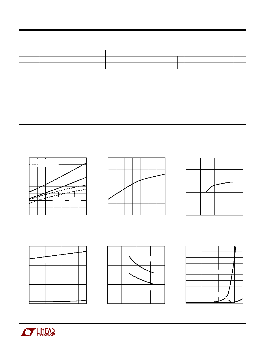
DS(ON)
vs Temperature
Oscillator Frequency
vs Temperature
Oscillator Frequency
vs Supply Voltage
TYPICAL PERFOR A CE CHARACTERISTICS
U
W
TEMPERATURE (
°
C)
50
0
50
100
125
SUPPLY CURRENT (
µ
A)
1875 G04
300
250
200
150
100
50
0
PULSE SKIPPING MODE
BURST MODE
V
IN
= 3.6V
DC Supply Current
vs Temperature
INPUT VOLTAGE (V)
0
2
4
6
8
R
DS(ON)
(
)
1875 G05
0.6
0.5
0.4
0.3
0.2
0.1
0
SYNCHRONOUS SWITCH
MAIN SWITCH
TEMPERATURE (
°
C)
50
0
50
100
125
SWITCH LEAKAGE (
µ
A)
1875 G06
10
9
8
7
6
5
4
3
2
1
0
MAIN SWITCH
SYNCHRONOUS SWITCH
V
IN
= 7V
RUN = 0V
R
DS(ON)
vs Input Voltage
Switch Leakage Current
vs Temperature
4
LTC1875
1875f
TYPICAL PERFOR A CE CHARACTERISTICS
U
W
LOAD CURRENT (mA)
0
500
1000
1500
2000
OUTPUT VOLTAGE (V)
1875 G07
1.84
1.82
1.80
1.78
1.76
1.74
1.72
1.70
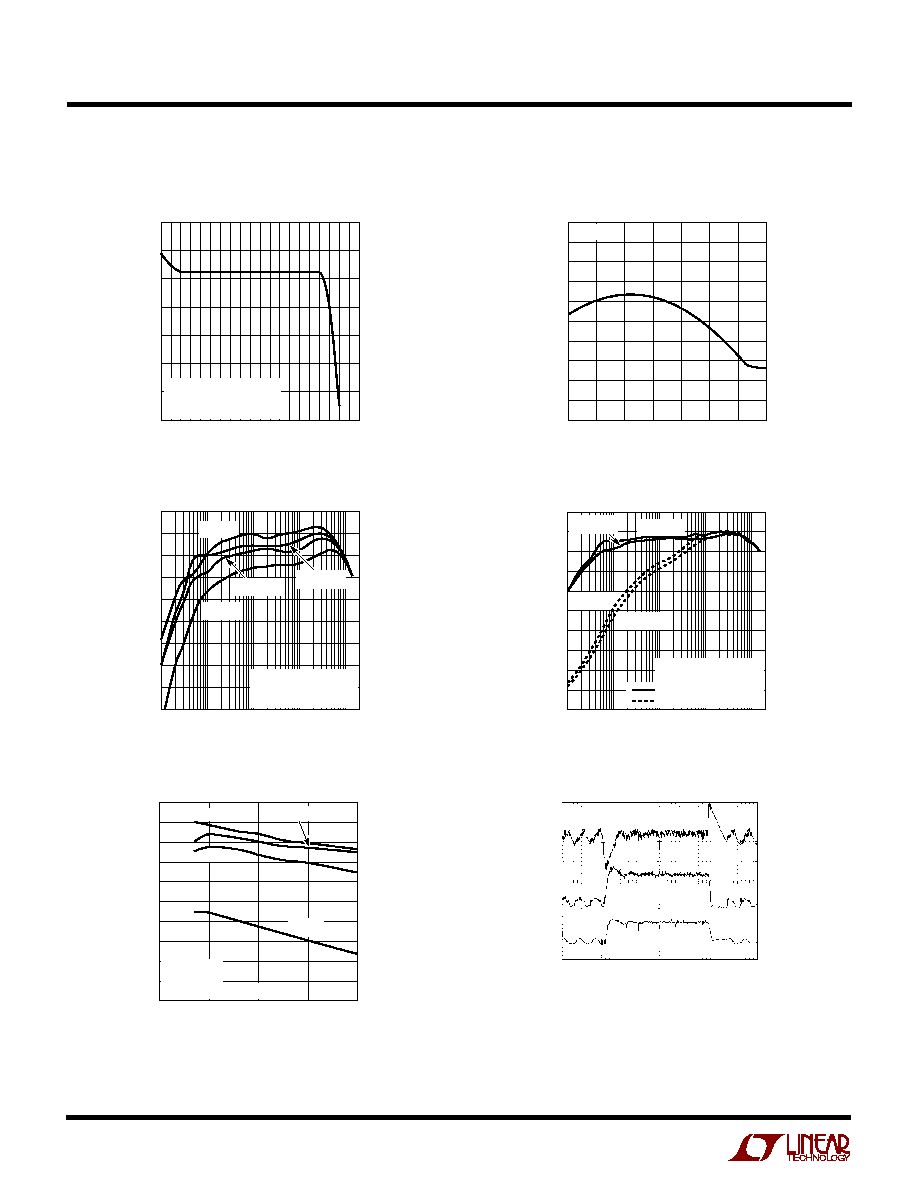
Burst Mode OPERATION
V
IN
= 3.6V
L = 4.7
µ
H
Output Voltage vs Load Current
Load Step (Burst Mode Operation)
V
OUT
100mV/DIV
I
L
1A/DIV
I
TH
1V/DIV
50
µ
s/DIV
1875 G08
V
IN
= 3.6V
C
IN
= 22
µ
F
V
OUT
= 1.5V
C
OUT
= 47
µ
F
L = 6.8
µ
H
I
LOAD
= 200mA to 1700mA
TEMPERATURE (
°
C)
50
25
0
25
50
75
100
125
REFERENCE VOLTAGE (mV)
1875 G13
805
804
803
802
801
800
799
798
797
796
795
V
IN
= 6V
OUTPUT CURRENT (mA)
EFFICIENCY (%)
95
90
85
80
75
70
65
60
55
50
0.1
10
100
1875 G14
1
1000
V
IN
= 6V
V
IN
= 4.2V
V
IN
= 3V
V
IN
= 3.6V
V
OUT
= 1.8V
L = 4.7
µ
H
Burst Mode OPERATION
OUTPUT CURRENT (mA)
EFFICIENCY (%)
100
90
80
70
60
50
40
30
20
10
0
0.1
10
100
1875 G15
1
1000
V
IN
= 3.6V
V
OUT
= 1.8V
L = 4.7
µ
H
Burst Mode OPERATION
PULSE SKIPPING MODE
V
IN
= 4.2V
V
IN
= 3.6V
V
IN
= 4.2V
INPUT VOLTAGE (V)
EFFICIENCY (%)
100
95
90
85
80
75
70
65
60
55
50
2
1875 G16
3
4
5
6
V
OUT
= 2.5V
L = 6.8
µ
H
Burst Mode OPERATION
100mA
1mA
0.1mA
10mA
Reference Voltage vs
Temperature
Efficiency vs Output Current
Efficiency vs Input Voltage
Efficiency vs Output Current
5
LTC1875
1875f
Load Step Response (Pulse
Skipping Mode)
Pulse Skipping Mode Operation
Burst Mode Operation
Soft-Start with Shorted Output
TYPICAL PERFOR A CE CHARACTERISTICS
U
W
I
L
200mA/DIV
V
OUT
100mV/DIV
SW
5V/DIV
V
OUT
100mV/DIV
I
L
1A/DIV
I
TH
1V/DIV
I
L
200mA/DIV
V
OUT
100mV/DIV
SW
5V/DIV
I
VIN
500mA/DIV
RUN/SS
1V/DIV
100
µ
s/DIV
1875 G09
V
IN
= 3.6V
C
IN
= 22
µ
F
V
OUT
= 1.5V
C
OUT
= 47
µ
F
L = 6.8
µ
H
I
LOAD
= 200mA to 1700mA
1
µ
s/DIV
1875 G10
V
IN
= 4.2V
C
IN
= 22
µ
F
V
OUT
= 2.5V
C
OUT
= 47
µ
F
L = 6.8
µ
H
I
LOAD
= 50mA
25
µ
s/DIV
1875 G11
V
IN
= 4.2V
C
IN
= 22
µ
F
V
OUT
= 2.5V
C
OUT
= 47
µ
F
L = 6.8
µ
H
I
LOAD
= 50mA
5ms/DIV
1875 G12
V
IN
= 3.6V
C
IN
= 22
µ
F
V
OUT
= 0V
C
OUT
= 47
µ
F
L = 6.8
µ
H
I
LOAD
= 0A