1929f.pm6
1
LTC1929/LTC1929-PG
2-Phase, High Efficiency,
Synchronous Step-Down
Switching Regulators
, LTC and LT are registered trademarks of Linear Technology Corporation.
OPTI-LOOP is a trademark of Linear Technology Corporation.
The LTC
®
1929/LTC1929-PG are 2-phase, single output,
synchronous step-down current mode switching regula-
tor controllers that drive N-channel external power MOSFET
stages in a phase-lockable fixed frequency architecture.
The 2-phase controllers drive their two output stages out
of phase at frequencies up to 300kHz to minimize the RMS
ripple currents in both input and output capacitors. The
2-phase technique effectively multiplies the fundamental
frequency by two, improving transient response while
operating each channel at an optimum frequency for
efficiency. Thermal design is also simplified.
An internal differential amplifier provides true remote
sensing of the regulated supply's positive and negative
output terminals as required by high current applications.
The RUN/SS pin provides soft-start and a defeatable,
timed, latched short-circuit shutdown to shut down both
channels. Internal foldback current limit provides protec-
tion for the external synchronous MOSFETs in the event of
an output fault. OPTI-LOOP compensation allows the
transient response to be optimized over a wide range of
output capacitance and ESR values.
Figure 1. High Current 2-Phase Step-Down Converter
s
Desktop Computers
s
Internet/Network Servers
s
Large Memory Arrays
s
DC Power Distribution Systems
s
2-Phase Single Output Controller
s
Reduces Required Input Capacitance and Power
Supply Induced Noise
s
Current Mode Control Ensures Current Sharing
s
Phase-Lockable Fixed Frequency: 150kHz to 300kHz
s
True Remote Sensing Differential Amplifier
s
OPTI-LOOP
TM
Compensation Improves Transient
Response
s
±
1% Output Voltage Accuracy
s
Power Good Output Voltage Monitor (LTC1929-PG)
s
Wide V
IN
Range: 4V to 36V Operation
s
Very Low Dropout Operation: 99% Duty Cycle
s
Adjustable Soft-Start Current Ramping
s
Internal Current Foldback
s
Short-Circuit Shutdown Timer with Defeat Option
s
Overvoltage Soft-Latch Eliminates Nuisance Trips
s
Available in 28-Lead SSOP Package
FEATURES
DESCRIPTIO
U
APPLICATIO S
U
TYPICAL APPLICATIO
U
1929 F01
TG1
BOOST1
SW1
BG1
PGND
SENSE1
+
SENSE1
TG2
BOOST2
SW2
BG2
INTV
CC
SENSE2
+
SENSE2
V
IN
RUN/SS
EAIN
I
TH
V
DIFFOUT
V
OS
V
OS
+
LTC1929
SGND
0.1
µ
F
0.1
µ
F
16k
1000pF
10
10k
16k
+
10
µ
F
35V
CERAMIC
×
4
+
C
OUT
1000
µ
F
4V
×
2
V
OUT
1.6V/40A
L1
1
µ
H
0.002
V
IN
5V TO 28V
L2
1
µ
H
D2
D1
0.47
µ
F
0.47
µ
F
100pF
10
µ
F
0.002
C
OUT
: T510E108K004AS L1, L2: CEPH149-1ROMC
2
LTC1929/LTC1929-PG
ORDER PART
NUMBER
LTC1929CG
LTC1929CG-PG
LTC1929IG
LTC1929IG-PG
ABSOLUTE AXI U
RATI GS
W
W
W
U
PACKAGE/ORDER I FOR ATIO
U
U
W
T
JMAX
= 125
°
C,
JA
= 95
°
C/W
Consult factory for Military grade parts.
ELECTRICAL CHARACTERISTICS
The
q
denotes the specifications which apply over the full operating
temperature range, otherwise specifications are at T
A
= 25
°
C. V
IN
= 15V, V
RUN/SS
= 5V unless otherwise noted.
(Note 1)
Input Supply Voltage (V
IN
).........................36V to 0.3V
Topside Driver Voltages (BOOST1,2) .........42V to 0.3V
Switch Voltage (SW1, 2) .............................36V to 5 V
SENSE1
+
, SENSE2
+
, SENSE1
,
SENSE2
Voltages ........................ (1.1)INTV
CC
to 0.3V
EAIN, V
OS
+
, V
OS
, EXTV
CC
, INTV
CC
,
RUN/SS, AMPMD Voltages .......................... 7V to 0.3V
Boosted Driver Voltage (BOOST-SW) .......... 7V to 0.3V
PLLFLTR, PLLIN, V
DIFFOUT
Voltages .... INTV
CC
to 0.3V
I
TH
Voltage ................................................2.7V to 0.3V
Peak Output Current <1
µ
s(TGL1,2, BG1,2) ................ 3A
INTV
CC
RMS Output Current ................................ 50mA
Operating Ambient Temperature Range
LTC1929C .................................................. 0
°
C to 85
°
C
LTC1929I .............................................. 40
°
C to 85
°
C
Junction Temperature (Note 2) ............................. 125
°
C
Storage Temperature Range ................. 65
°
C to 150
°
C
Lead Temperature (Soldering, 10 sec).................. 300
°
C
SYMBOL
PARAMETER
CONDITIONS
MIN
TYP
MAX
UNITS
Main Control Loop
V
EAIN
Regulated Feedback Voltage
(Note 3); I
TH
Voltage = 1.2V
q
0.792
0.800
0.808
V
V
SENSEMAX
Maximum Current Sense Threshold
V
SENSE
= 5V
q
62
75
88
mV
V
SENSE1, 2
= 5V, LTC1929 Only
65
75
85
mV
I
INEAIN
Feedback Current
(Note 3)
5
50
nA
V
LOADREG
Output Voltage Load Regulation
(Note 3)
Measured in Servo Loop; I
TH
Voltage = 0.7V
q
0.05
0.5
%
Measured in Servo Loop; I
TH
Voltage = 2V
q
0.1
0.5
%
V
REFLNREG
Reference Voltage Line Regulation
V
IN
= 3.6V to 30V (Note 3)
0.002
0.02
%/V
V
OVL
Output Overvoltage Threshold
Measured at V
EAIN
0.84
0.86
0.88
V
UVLO
Undervoltage Lockout
V
IN
Ramping Down
3
3.5
4
V
g
m
Transconductance Amplifier g
m
I
TH
= 1.2V; Sink/Source 5
µ
A; (Note 3)
3
mmho
g
mOL
Transconductance Amplifier Gain
I
TH
= 1.2V; (g
m
xZ
L
; No Ext Load); (Note 3)
1.5
V/mV
I
Q
Input DC Supply Current
(Note 4)
Normal Mode
EXTV
CC
Tied to V
OUT
; V
OUT
= 5V
470
µ
A
Shutdown
V
RUN/SS
= 0V
20
40
µ
A
I
RUN/SS
Soft-Start Charge Current
V
RUN/SS
= 1.9V
0.5
1.2
µ
A
V
RUN/SS
RUN/SS Pin ON Threshold
V
RUN/SS
Rising
1.0
1.5
1.9
V
V
RUN/SSLO
RUN/SS Pin Latchoff Arming
V
RUN/SS
Rising from 3V
4.1
4.5
V
1
2
3
4
5
6
7
8
9
10
11
12
13
14
TOP VIEW
G PACKAGE
28-LEAD PLASTIC SSOP
*PGOOD ON LTC1929-PG
28
27
26
25
24
23
22
21
20
19
18
17
16
15
RUN/SS
SENSE1
+
SENSE1
EAIN
PLLFLTR
PLLIN
NC
I
TH
SGND
V
DIFFOUT
V
OS
V
OS
+
SENSE2
SENSE2
+
NC
TG1
SW1
BOOST1
V
IN
BG1
EXTV
CC
INTV
CC
PGND
BG2
BOOST2
SW2
TG2
AMPMD*
3
LTC1929/LTC1929-PG
ELECTRICAL CHARACTERISTICS
The
q
denotes the specifications which apply over the full operating
temperature range, otherwise specifications are at T
A
= 25
°
C. V
IN
= 15V, V
RUN/SS
= 5V unless otherwise noted.
SYMBOL
PARAMETER
CONDITIONS
MIN
TYP
MAX
UNITS
I
SCL
RUN/SS Discharge Current
Soft Short Condition V
EAIN
= 0.5V;
0.5
2.0
4.0
µ
A
V
RUN/SS
= 4.5V
I
SDLHO
Shutdown Latch Disable Current
V
EAIN
= 0.5V
1.6
5
µ
A
I
SENSE
Total Sense Pins Source Current
Each Channel: V
SENSE1
, 2
= V
SENSE1
+
, 2
+ = 0V
85
60
µ
A
DF
MAX
Maximum Duty Factor
In Dropout
98
99.5
%
Top Gate Transition Time:
TG1, 2 t
r
Rise Time
C
LOAD
= 3300pF
30
90
ns
TG1, 2 t
f
Fall Time
C
LOAD
= 3300pF
40
90
ns
Bottom Gate Transition Time:
BG1, 2 t
r
Rise Time
C
LOAD
= 3300pF
30
90
ns
BG1, 2 t
f
Fall Time
C
LOAD
= 3300pF
20
90
ns
TG/BG t
1D
Top Gate Off to Bottom Gate On Delay
Synchronous Switch-On Delay Time
C
LOAD
= 3300pF Each Driver
90
ns
BG/TG t
2D
Bottom Gate Off to Top Gate On Delay
Top Switch-On Delay Time
C
LOAD
= 3300pF Each Driver
90
ns
t
ON(MIN)
Minimum On-Time
Tested with a Square Wave (Note 6)
180
ns
Internal V
CC
Regulator
V
INTVCC
Internal V
CC
Voltage
6V < V
IN
< 30V; V
EXTVCC
= 4V
4.8
5.0
5.2
V
V
LDO
INT
INTV
CC
Load Regulation
I
CC
= 0 to 20mA; V
EXTVCC
= 4V
0.2
1.0
%
V
LDO
EXT
EXTV
CC
Voltage Drop
I
CC
= 20mA; V
EXTVCC
= 5V
120
240
mV
V
LDO
EXT-PG
EXTV
CC
Voltage Drop
I
CC
= 20mA, V
EXTVCC
= 5V, LTC1929-PG
80
160
mV
V
EXTVCC
EXTV
CC
Switchover Voltage
I
CC
= 20mA, EXTV
CC
Ramping Positive
q
4.5
4.7
V
V
LDOHYS
EXTV
CC
Switchover Hysteresis
I
CC
= 20mA, EXTV
CC
Ramping Negative
0.2
V
Oscillator and Phase-Locked Loop
f
NOM
Nominal Frequency
V
PLLFLTR
= 1.2V
190
220
250
kHz
f
LOW
Lowest Frequency
V
PLLFLTR
= 0V
120
140
160
kHz
f
HIGH
Highest Frequency
V
PLLFLTR
2.4V
280
310
360
kHz
R
PLLIN
PLLIN
Input Resistance
50
k
I
PLLFLTR
Phase Detector Output Current
Sinking Capability
f
PLLIN
< f
OSC
15
µ
A
Sourcing Capability
f
PLLIN
> f
OSC
15
µ
A
R
RELPHS
Controller 2-Controller 1 Phase
180
Deg
PGOOD Output (LTC1929-PG Only)
V
PGL
PGOOD Voltage Low
I
PGOOD
= 2mA
0.1
0.3
V
I
PGOOD
PGOOD Leakage Current
V
PGOOD
= 5V
±
1
µ
A
V
PG
PGOOD Trip Level
V
EAIN
with Respect to Set Output Voltage
V
EAIN
Ramping Negative
6
7.5
9.5
%
V
EAIN
Ramping Positive
6
7.5
9.5
%
Differential Amplifier/Op Amp Gain Block (Note 5)
A
DA
Gain
Differential Amp Mode
0.995
1
1.005
V/V
CMRR
DA
Common Mode Rejection Ratio
Differential Amp Mode; 0V < V
CM
< 5V
46
55
dB
R
IN
Input Resistance
Differential Amp Mode; Measured at V
OS
+ Input
80
k
V
OS
Input Offset Voltage
Op Amp Mode; V
CM
= 2.5V; V
DIFFOUT
= 5V;
6
mV
I
DIFFOUT
= 1mA (LTC1929 Only)
4
LTC1929/LTC1929-PG
SYMBOL
PARAMETER
CONDITIONS
MIN
TYP
MAX
UNITS
I
B
Input Bias Current
Op Amp Mode (LTC1929 Only)
30
200
nA
A
OL
Open Loop DC Gain
Op Amp Mode; 0.7V
V
DIFFOUT
< 10V
5000
V/mV
(LTC1929 Only)
V
CM
Common Mode Input Voltage Range
Op Amp Mode (LTC1929 Only)
0
3
V
CMRR
OA
Common Mode Rejection Ratio
Op Amp Mode; 0V < V
CM
< 3V (LTC1929 Only)
70
90
dB
PSRR
OA
Power Supply Rejection Ratio
Op Amp Mode; 6V < V
IN
< 30V (LTC1929 Only)
70
90
dB
I
CL
Maximum Output Current
Op Amp Mode; V
DIFFOUT
= 0V (LTC1929 Only)
10
35
mA
V
O(MAX)
Maximum Output Voltage
Op Amp Mode; I
DIFFOUT
= 1mA (LTC1929 Only)
10
11
V
GBW
Gain-Bandwidth Product
Op Amp Mode; I
DIFFOUT
= 1mA (LTC1929 Only)
2
MHz
SR
Slew Rate
Op Amp Mode; R
L
= 2k (LTC1929 Only)
5
V/
µ
s
ELECTRICAL CHARACTERISTICS
temperature range, otherwise specifications are at T
A
= 25
°
C. V
IN
= 15V, V
RUN/SS
= 5V unless otherwise noted.
Note 5: When the AMPMD pin is high (default for the LTC1929-PG), the
LTC1929 IC pins are connected directly to the internal op amp inputs.
When the AMPMD pin is low, internal MOSFET switches connect four
40k resistors around the op amp to create a standard unity-gain
differential amp.
Note 6: Minimum on-time condition corresponds to the on inductor
peak-to-peak ripple current
40% of I
MAX
(see minimum on-time
considerations in the Applications Information section).
Note 1: Absolute Maximum Ratings are those values beyond which the
life of a device may be impaired.
Note 2: T
J
is calculated from the ambient temperature T
A
and power
dissipation P
D
according to the following formulas:
LTC1929CG: T
J
= T
A
+ (P
D
· 95
°
C/W)
Note 3: The LTC1929 is tested in a feedback loop that servos V
ITH
to a
specified voltage and measures the resultant V
EAIN
.
Note 4: Dynamic supply current is higher due to the gate charge being
delivered at the switching frequency. See Applications Information.
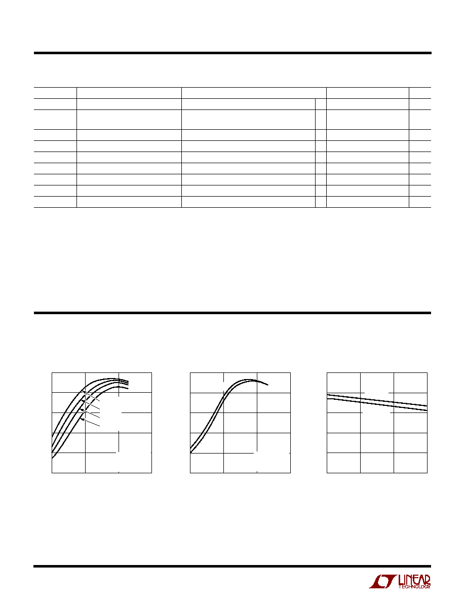
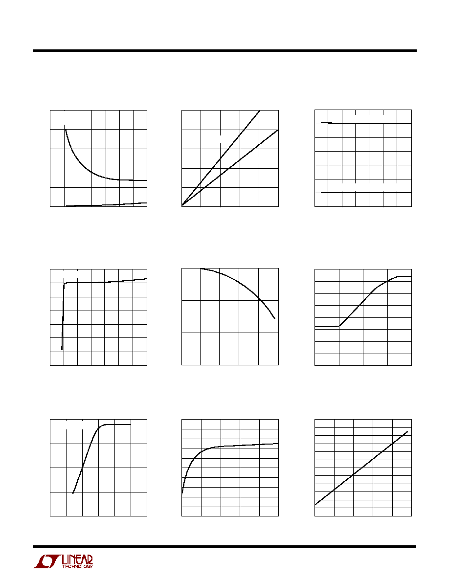
TYPICAL PERFOR A CE CHARACTERISTICS
U
W
Efficiency vs Output Current
(Figure 13)
OUTPUT CURRENT (A)
0.1
EFFICIENCY (%)
100
80
60
40
20
0
1929 G01
1
10
100
V
OUT
= 2V
V
EXTVCC
= 0V
FREQ = 200kHz
V
IN
= 5V
V
IN
= 8V
V
IN
= 12V
V
IN
= 20V
OUTPUT CURRENT (A)
0.1
EFFICIENCY (%)
40
60
1929 G02
20
0
10
1
100
100
80
V
IN
= 12V
V
OUT
= 2V
FREQ = 200kHz
V
EXTVCC
= 5V
V
EXTVCC
= 0V
V
IN
(V)
5
EFFICIENCY (%)
100
90
80
70
60
50
1929 G03
10
15
20
V
EXTVCC
= 5V
I
OUT
= 20A
V
OUT
= 2V
V
OUT
= 1.6V
Efficiency vs Output Current
(Figure 13)
Efficiency vs V
IN
(Figure 13)
The
q
denotes the specifications which apply over the full operating
5
LTC1929/LTC1929-PG
TYPICAL PERFOR A CE CHARACTERISTICS
U
W
Supply Current vs Input Voltage
and Mode
EXTV
CC
Voltage Drop
INTV
CC
and EXTV
CC
Switch
Voltage vs Temperature
INPUT VOLTAGE (V)
0
5
0
SUPPLY CURRENT (
µ
A)
400
1000
10
20
25
1929 G04
200
800
600
15
30
35
ON
SHUTDOWN
V
OUT
= 5V
V
EXTVCC
= V
OUT
CURRENT (mA)
0
EXTV
CC
VOLTAGE DROP (mV)
150
200
250
40
1929 G05
100
50
0
10
20
30
50
LTC1929
LTC1929-PG
TEMPERATURE (
°
C)
50
INTV
CC
AND EXTV
CC
SWITCH VOLTAGE (V)
4.95
5.00
5.05
25
75
1929 G06
4.90
4.85
25
0
50
100
125
4.80
4.70
4.75
INTV
CC
VOLTAGE
EXTV
CC
SWITCHOVER THRESHOLD
Maximum Current Sense Threshold
vs Percent on Nominal Output
Voltage (Foldback)
Internal 5V LDO Line Reg
Maximum Current Sense Threshold
vs Duty Factor
INPUT VOLTAGE (V)
0
4.8
4.9
5.1
15
25
1929 G07
4.7
4.6
5
10
20
30
35
4.5
4.4
5.0
INTV
CC
VOLTAGE (V)
I
LOAD
= 1mA
DUTY FACTOR (%)
0
0
V
SENSE
(mV)
25
50
75
20
40
60
80
1929 G08
100
PERCENT ON NOMINAL OUTPUT VOLTAGE (%)
0
V
SENSE
(mV)
40
50
60
100
1929 G09
30
20
0
25
50
75
10
80
70
Maximum Current Sense Threshold
vs Sense Common Mode Voltage
Maximum Current Sense Threshold
vs V
RUN/SS
(Soft-Start)
Current Sense Threshold
vs I
TH
Voltage
V
RUN/SS
(V)
0
0
V
SENSE
(mV)
20
40
60
80
1
2
3
4
1929 G10
5
6
V
SENSE(CM)
= 1.6V
COMMON MODE VOLTAGE (V)
0
V
SENSE
(mV)
72
76
80
4
1929 G11
68
64
60
1
2
3
5
V
ITH
(V)
0
V
SENSE
(mV)
30
50
70
90
2
1929 G12
10
10
20
40
60
80
0
20
30
0.5
1
1.5
2.5