 | ÐлекÑÑоннÑй компоненÑ: LTC1983-X | СкаÑаÑÑ:  PDF PDF  ZIP ZIP |
1983f.pm6
LTC1983-3/LTC1983-5
1
sn1983 1983fs
The LTC
®
1983-3 and LTC1983-5 are inverting charge
pump DC/DC converters that produce negative regulated
outputs. The parts require only three tiny external capaci-
tors and can provide up to 100mA of output current. The
devices can operate in open loop mode (creating a V
IN
supply) or regulated output mode depending on the input
supply voltage and the output current.
The LTC1983-3/LTC1983-5 have many useful features for
portable applications including very low quiescent current
(25
µ
A typical) and a zero current shutdown mode pro-
grammed through the SHDN pin.
The LTC1983-3/LTC1983-5 are over-temperature and
short-circuit protected. The parts are available in a 6-pin
low profile (1mm) ThinSOT package.
s
3V Generation in Single-Supply Systems
s
Portable Equipment
s
LCD Bias Supplies
s
GaAs FET Bias Supplies
s
Fixed Output Voltages: 3V, 5V or Low Noise V
IN
to V
IN
Inverted Output
s
±
4% Output Voltage Accuracy
s
Low Quiesient Current: 25
µ
A
s
100mA Output Current Capability
s
3V to 5.5V Operating Voltage Range (LTC1983-3)
s
2.3V to 5.5V Operating Voltage Range (LTC1983-5)
s
Internal 900kHz Oscillator
s
"Zero Current" Shutdown
s
Short-Circuit and Over-Temperature Protected
s
Low Profile (1mm) ThinSOT
TM
Package
100mA Regulated
Charge-Pump Inverters
in ThinSOT
, LTC and LT are registered trademarks of Linear Technology Corporation.
ThinSOT is a trademark of Linear Technology Corporation.
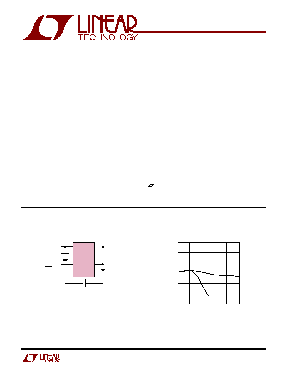
V
IN
SHDN
C
+
V
OUT
GND
C
LTC1983-3
V
IN
3V TO 5.5V
V
OUT
= 3V
I
OUT
= UP TO 100mA
C
OUT
10
µ
F
C
IN
10
µ
F
C
FLY
1
µ
F
OFF ON
C
FLY
: TAIYO YUDEN LMK212BJ105
C
IN
, C
OUT
: TAIYO YUDEN JMK316BJ106ML
1983-3 TA01
V
OUT
vs I
OUT
I
OUT
(mA)
0
V
OUT
(V)
3.3
3.2
3.1
3.0
2.9
2.8
2.7
20
40
60
80
1983 TA02
100
V
IN
= 5V
V
IN
= 3.3V
DESCRIPTIO
U
FEATURES
APPLICATIO S
U
TYPICAL APPLICATIO
U
3V at 100mA DC/DC Converter
LTC1983-3/LTC1983-5
2
sn1983 1983fs
V
IN
to GND ................................................... 0.3V to 6V
SHDN Voltage .............................................. 0.3V to 6V
V
OUT
to GND (LTC1983-3) .................. 0.2V to V
OUT
Max
V
OUT
to GND (LTC1983-5) .................. 0.2V to V
OUT
Max
I
OUT
Max ............................................................. 125mA
Output Short-Circuit Duration .......................... Indefinite
Operating Temperature Range (Note 2) ...40
°
C to 85
°
C
Storage Temperature Range ................. 65
°
C to 125
°
C
Lead Temperature (Soldering, 10 sec).................. 300
°
C
ORDER PART
NUMBER
S6 PART
MARKING
T
JMAX
= 125
°
C,
JA
= 256
°
C/W
Consult LTC Marketing for parts specified with wider operating temperature ranges.
LTPC
LTYB
LTC1983ES6-3
LTC1983ES6-5
ABSOLUTE AXI U
RATI GS
W
W
W
U
PACKAGE/ORDER I FOR ATIO
U
U
W
(Note 1)
ELECTRICAL CHARACTERISTICS
Burst Mode is a registered trademark of Linear Technology
Corporation.
Note 1: Absolute Maximum Ratings are those values beyond
which the life of a device may be impaired.
The
q
denotes the specifications which apply over the full operating
temperature range, otherwise specifications are at T
A
= 25
°
C. V
IN
= 5V, C
FLY
= 1
µ
F, C
OUT
= 10
µ
F
unless otherwise noted.
PARAMETER
CONDITIONS
MIN
TYP
MAX
UNITS
V
IN
Operating Voltage (Regulated Output Mode) (LTC1983-3)
q
3.0
5.5
V
V
IN
Min Startup Voltage
2.3
V
V
OUT
(LTC1983-3)
V
IN
3.3V, I
OUT
25mA
q
2.88
3
3.12
V
V
IN
5V, I
OUT
100mA
q
2.88
3
3.12
V
V
OUT
(LTC1983-5)
V
IN
5V, V
IN
5V
I
OUT
· R
OUT
q
4.8
5
5.2
V
V
IN
Operating Current
V
IN
5.5V, I
OUT
= 0
µ
A, SHDN = V
IN
q
25
60
µ
A
V
IN
Operating Current (Open-Loop Mode) (LTC1983-5)
V
IN
= 3.3V
2.5
mA
V
IN
= 4.75V
4
mA
V
IN
Shutdown Current
SHDN = 0V, V
IN
5.5V
q
0.1
1
µ
A
Output Ripple
3.3
V
IN
5.5
60
mV
P-P
Open-Loop Output Impedance (LTC1983-3): R
OUT
V
IN
= 3.3V, V
OUT
= 3V
11
Open-Loop Output Impedance (LTC1983-5): R
OUT
V
IN
= 3.3V, I
OUT
50mA
11
V
IN
= 5V, I
OUT
60mA
8.5
Oscillator Frequency
(Non-Burst Mode
®
Operation)
900
kHz
SHDN Input High
q
1.1
V
SHDN Input Low
q
0.3
V
SHDN Input Current
V
SHDN
= 5.5V
q
2.2
4
µ
A
V
CC
1
V
OUT
2
C
+
3
6 SHDN
5 GND
4 C
TOP VIEW
S6 PACKAGE
6-LEAD PLASTIC SOT-23
Note 2: The LTC1983E-3/LTC1983E-5 are guaranteed to meet
performance specifications from 0
°
C to 70
°
C. Specifications over the
40
°
C to 85
°
C operating temperature range are assured by design,
characterization and correlation with statistical process controls.
LTC1983-3/LTC1983-5
3
sn1983 1983fs
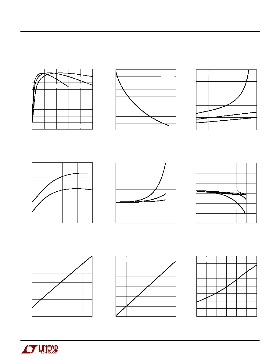
Output Impedance vs
Input Voltage
Output Impedance
vs I
OUT
(LTC1983-5)
Efficiency vs I
OUT
(LTC1983-5)
TYPICAL PERFOR A CE CHARACTERISTICS
U
W
Efficiency vs I
OUT
I
OUT
(mA)
0
EFFICIENCY (%)
40
80
100
90
80
70
60
50
40
30
20
10
0
1983 G01
20
60
V
IN
= 2.3V
V
IN
= 3.3V
V
IN
= 5V
T
A
= 25
°
C
V
IN
(V)
2.35
R
OUT
(
)
4.35
12.5
12.0
11.5
11.0
10.5
10.0
9.5
9.0
8.5
8.0
1983 TA02
3.35
5.35
R
OUT
I
OUT
= 25mA
T
A
= 25
°
C
I
OUT
(mA)
0
R
OUT
(
)
40
80
100
30
25
20
15
10
5
1983 G03
20
60
V
IN
= 2.3V
V
IN
= 3.3V
V
IN
= 5V
T
A
= 25
°
C
I
OUT
(mA)
0.01
100
75
50
25
0
10
1983 GO4
0.1
1
100
EFFICIENCY (%)
V
IN
= 5V
V
IN
= 3.3V
V
OUT
= 3V
T
A
= 25
°
C
OUTPUT CURRENT (mA)
0
2.1
2.3
2.5
2.7
2.9
3.1
3.3
3.5
60
100
1983 G05
20
40
80
120
V
OUT
(V)
120
°
C
40
°
C, 0
°
C, 40
°
C
80
°
C
OUTPUT CURRENT (mA)
0
2.7
V
OUT
(
V)
2.8
2.9
3.0
3.1
3.3
20
40
60
80
1983 G06
100
120
3.2
40
°
C 0
°
C
40
°
C
80
°
C
V
IN
= 5V
3V
OUT
vs I
OUT
Over Temperature
3V
OUT
vs I
OUT
Over Temperature
(V
IN
= 5V)
Open-Loop Current
vs Temperature (LTC1983-5)
TEMPERATURE (
°
C)
40
4.9
4.7
4.5
4.3
4.1
3.9
3.7
3.5
1983 G07
10
60
110
I
IN
(mA)
V
IN
= 5V
Burst Mode Current
vs Temperature (LTC1983-3)
TEMPERATURE (
°
C)
40
I
IN
(
µ
A)
25
30
35
1983 G08
20
15
10
10
60
40
45
50
110
V
IN
= 5V
Open-Loop Input Current
vs V
IN
(LTC1983-5)
V
IN
(V)
2.3
1.5
I
IN
(mA)
2.0
2.5
3.0
3.5
4.5
2.8
3.3
3.3
4.3
1983 G09
4.8
4.0
T
A
= 25
°
C
LTC1983-3/LTC1983-5
4
sn1983 1983fs
TYPICAL PERFOR A CE CHARACTERISTICS
U
W
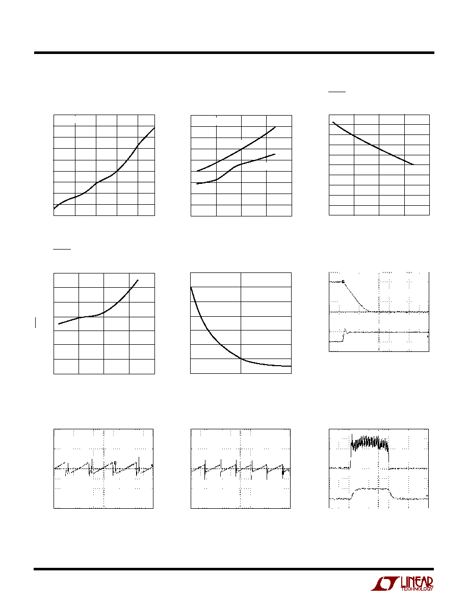
Burst Mode Input Current
vs V
IN
(LTC1983-3)
V
IN
(V)
3.1
26.5
INPUT CURRENT (
µ
A)
27.0
28.0
28.5
29.0
4.1
5.1
5.5
31.0
1983 G10
27.5
3.6
4.6
29.5
30.0
30.5
T
A
= 25
°
C
TEMPERATURE (
°
C)
50
R
OUT
(
)
10
12
14
150
1983 G11
8
6
0
0
50
100
4
2
18
16
V
IN
= 5V
V
IN
= 3V
I
OUT
= 10mA
TEMPERATURE (
°
C)
50
0
V
THRESHOLD
(V)
0.1
0.3
0.4
0.5
1.0
0.7
0
50
1983 G12
0.2
0.8
0.9
0.6
100
150
R
OUT
vs Temperature
(I
OUT
= 10mA)
SHDN Pin Threshold Voltage
vs Temperature
SHDN Pin Input Current
vs Temperature
R
OUT
vs C
FLY
(V
IN
= 5V)
TEMPERATURE (
°
C)
50
2.0
2.5
3.5
100
1983 G13
1.5
1.0
0
50
150
0.5
0
3.0
I
SHDN
C
FLY
(
µ
F)
0.01
1400
V
IN
= 5V
T
A
= 25
°
C
1200
1000
800
600
400
200
1983 G14
0.1
1
0
R
OUT
(
)
V
OUT
Start-Up into 100mA
Resistive Load
V
OUT
Ripple at 100mA Load
V
OUT
Ripple at 30mA Load
V
OUT
Load Step Reponse from
I
OUT
= 0 to I
OUT
= 100mA
V
OUT
1V
V
IN
5V
V
OUT
20mV
50
µ
s/DIV
1983 G15
1
µ
s/DIV
1983 G16
V
OUT
20mV
2.5
µ
s/DIV
1983 G17
V
OUT
20mV
100
µ
s/DIV
1983 G18
I
OUT
100mA
LTC1983-3/LTC1983-5
5
sn1983 1983fs
U
U
U
PI FU CTIO S
V
IN
(Pin 1): Charge Pump Input Voltage. May be between
2.3V and 5.5V. V
IN
should be bypassed with a
4.7
µ
F low
ESR capacitor as close as possible to the pin for best
performance.
V
OUT
(Pin 2): Regulated Output Voltage for the IC. V
OUT
should be bypassed with a
4.7
µ
F low ESR capacitor as
close as possible to the pin for best performance.
C
+
(Pin 3): Charge Pump Flying Capacitor Positive Termi-
nal. This node is switched between V
IN
and GND (It is
connected to V
CC
during shutdown).
C
(Pin 4): Charge Pump Flying Capacitor Negative Termi-
nal. This node is switched between GND and V
OUT
(It is
connected to GND during shutdown).
GND (Pin 5): Signal and Power Ground for the 6-Pin
SOT-23 package. This pin should be tied to a ground plane
for best performance.
SHDN (Pin 6): Shutdown. Grounding this pin shuts down
the IC. Tie to V
IN
to enable. This pin should not be pulled
above the V
IN
voltage or below GND.
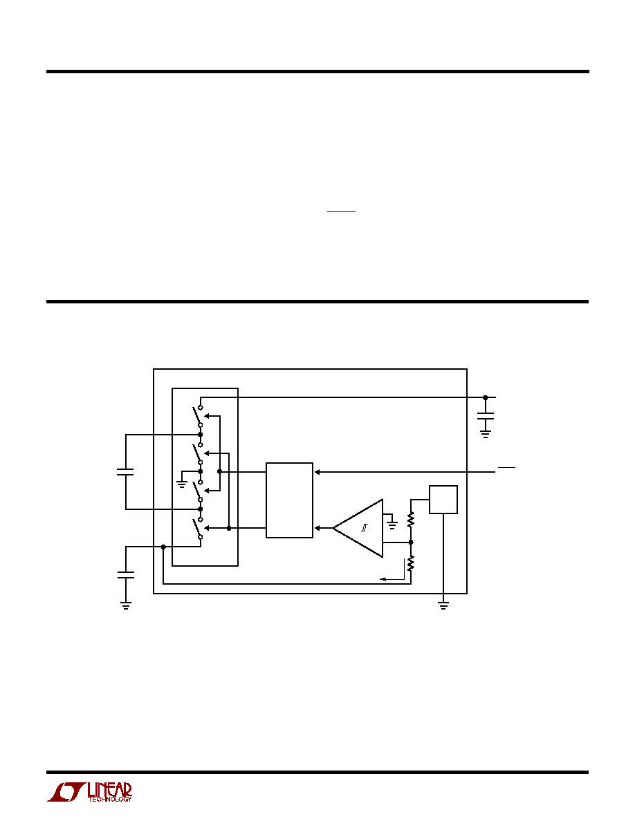
BLOCK DIAGRA
W
CONTROL
LOGIC
CLOCK2
CLOCK1
S1A
S2A
S1B
S2B
+
V
REF
CHARGE PUMP
SHDN
V
IN
C
IN
10
µ
F
C
FLY
1
µ
F
C
OUT
10
µ
F
LTC1983-X
C
+
C
V
OUT
COMP1
1
µ
A
1983 BD