 | –≠–ª–µ–∫—Ç—Ä–æ–Ω–Ω—ã–π –∫–æ–º–ø–æ–Ω–µ–Ω—Ç: LTC203 | –°–∫–∞—á–∞—Ç—å:  PDF PDF  ZIP ZIP |

1
LT1203/LT1205
150MHz Video Multiplexers
s
≠ 3dB Bandwidth: 150MHz
s
0.1dB Gain Flatness: 30MHz
s
Channel-to-Channel Switching Time: 25ns
s
Turn-On/Turn-Off Time: 25ns
s
High Slew Rate: 300V/
µ
s
s
Disabled Output Impedance: 10M
s
50mV Switching Transient
s
Channel Separation at 10MHz: > 90dB
s
Differential Gain: 0.02%
s
Differential Phase: 0.02
∞
s
Wide Supply Range:
±
5V to
±
15V
s
Output Short-Circuit Protected
s
Push-Pull Output
S
FEATURE
D
U
ESCRIPTIO
The LT1203 is a wideband 2-input video multiplexer
designed for pixel switching and broadcast quality rout-
ing. The LT1205 is a dual version that is configured as a
4-input, 2-output multiplexer.
These multiplexers act as SPDT video switches with 10ns
transition times at toggle rates up to 30MHz. The ≠ 3dB
bandwidth is 150MHz and 0.1dB gain flatness is 30MHz.
Many parts can be tied together at their outputs by using
the enable feature which reduces the power dissipation
and raises the output impedance to 10M
. Output capaci-
tance when disabled is only 3pF and the LT1203 peaks less
than 3dB into a 50pF load. Channel crosstalk and disable
isolation are greater than 90dB up to 10MHz. An on-chip
buffer interfaces to fast TTL or CMOS logic. Switching
transients are only 50mV with a 25ns duration. The
LT1203 and LT1205 outputs are protected against shorts
to ground.
The LT1203/LT1205 are manufactured using Linear
Technology's proprietary complementary bipolar process.
The LT1203 is available in both the 8-lead PDIP and SO
package while the LT1205 is available in the 16-lead
narrow body SO package.
U
A
O
PPLICATI
TYPICAL
+1
+1
+1
+1
LT1205
LOGIC
V
+
LOGIC
V
OUT
RED
V
OUT
GREEN
V
OUT
BLUE
LT1203 ∑ TA01
EN
RED 1
CHANNEL SELECT
RED 2
GREEN 1
GREEN 2
BLUE 1
BLUE 2
V
≠
V
≠
V
≠
EN
V
+
+1
+1
LT1203
LOGIC
EN
V
+
High Speed RGB MUX
Large-Signal Response
U
S
A
O
PPLICATI
s
Broadcast Quality Video Multiplexing
s
Picture-in-Picture Switching
s
HDTV
s
Computer Graphics
s
Title Generation
s
Video Crosspoint Matrices
s
Video Routers

2
LT1203/LT1205
A
U
G
W
A
W
U
W
A
R
BSOLUTE
XI
TI
S
Supply Voltage ......................................................
±
18V
Signal Input Current (Note 1) ............................
±
20mA
Logic Input Current (Note 2)..............................
±
50mA
Output Short-Circuit Duration (Note 3) ........ Continuous
Specified Temperature Range (Note 4) ....... 0
∞
C to 70
∞
C
Operating Temperature Range ............... ≠ 40
∞
C to 85
∞
C
Storage Temperature Range ................ ≠ 65
∞
C to 150
∞
C
Junction Temperature (Note 5) ............................ 150
∞
C
Lead Temperature (Soldering, 10 sec) ................. 300
∞
C
ORDER PART
NUMBER
LT1203CN8*
LT1203CS8*
S8 PART MARKING
1203
*See Note 4
Consult factory for Industrial and Military grade parts.
ORDER PART
NUMBER
LT1205CS*
T
JMAX
= 150
∞
C,
JA
= 100
∞
C/W
TOP VIEW
S PACKAGE
16-LEAD PLASTIC SOIC
1
2
3
4
5
6
7
8
16
15
14
13
12
11
10
9
V
INO
GND
V
IN1
V
≠
V
IN2
GND
V
IN3
V
≠
V
+
V
OUT1
EN1
LOGIC 1
V
+
V
OUT2
EN2
LOGIC 2
1
2
3
4
8
7
6
5
TOP VIEW
V
IN0
GND
V
IN1
V
≠
V
+
V
OUT
EN
LOGIC
N8 PACKAGE
8-LEAD PLASTIC DIP
S8 PACKAGE
8-LEAD PLASTIC SOIC
T
JMAX
= 150
∞
C,
JA
= 100
∞
C/W (N)
T
JMAX
= 150
∞
C,
JA
= 150
∞
C/W (S)
W
U
U
PACKAGE/ORDER I FOR ATIO
SYMBOL
PARAMETER
CONDITIONS
MIN
TYP
MAX
UNITS
V
OS
Output Offset Voltage
Any Input Selected
q
10
30
mV
Output Offset Matching
Between Outputs
q
0.3
5
mV
V
OS
/
T
Output Offset Drift
q
40
µ
V/
∞
C
I
IN
Input Current
q
0.6
5
µ
A
R
IN
Input Resistance
V
S
=
±
5V, V
IN
=
±
2V
q
1
5
M
V
S
=
±
15V, V
IN
=
±
2V
q
2
5
M
C
IN
Input Capacitance
Input Selected
2.6
pF
Input Deselected
2.6
pF
C
OUT
Disabled Output Capacitance
EN Pin Voltage
0.8V
2.8
pF
V
IN
Input Voltage (Note 1)
V
S
=
±
5V
q
±
2
±
2.8
V
V
S
=
±
15V
q
±
2
±
3.0
V
PSRR
Power Supply Rejection Ratio
V
S
=
±
4.5 to
±
15V
q
60
70
dB
Gain Error
V
S
=
±
15V, V
IN
=
±
2V, R
L
= 1k
q
2
4
%
V
S
=
±
15V, V
IN
=
±
2V, R
L
= 400
q
6
10
%
V
S
=
±
5V, V
IN
=
±
2V, R
L
= 1k
q
3
6
%
ELECTRICAL C
C
HARA TERISTICS
0
∞
C
T
A
70
∞
C,
±
5V
V
S
±
15V, R
L
= 1k, pulse tested, EN pin open or high, unless otherwise noted.

3
LT1203/LT1205
SYMBOL
PARAMETER
CONDITIONS
MIN
TYP
MAX
UNITS
SR
Slew Rate (Note 6)
180
300
V/
µ
s
FPBW
Full Power Bandwidth (Note 7)
V
OUT
= 2V
P-P
28.6
47.7
MHz
t
SEL
Channel-to-Channel Select Time (Note 8) R
L
= 10k
25
35
ns
Enable Time (Note 9)
R
L
= 1k
25
35
ns
Disable Time (Note 9)
R
L
= 1k
20
35
ns
t
r
, t
f
Small-Signal Rise and Fall Time
V
OUT
= 250mV
P-P
, 10% to 90%
2.6
ns
Propagation Delay
V
OUT
= 250mV
P-P
2.9
ns
Overshoot
V
OUT
= 250mV
P-P
5
%
Crosstalk (Note 10)
R
S
= 10
90
dB
Chip Disabled Crosstalk (Note 10)
R
L
= 10
, EN Pin Voltage
0.8V
110
dB
Channel Select Output Transient
All V
IN
= 0V
50
mV
P-P
t
S
Settling Time
1%, V
OUT
= 1V
30
ns
Differential Gain (Note 11)
V
S
=
±
15V, R
L
= 10k
0.02
%
Differential Phase (Note 11)
V
S
=
±
15V, R
L
= 10k
0.02
DEG
Insertion Loss
R
L
= 100k, C
L
= 30pF, V
OUT
= 500mV
P-P
, f = 1MHz
0.02
dB
ELECTRICAL C
C
HARA TERISTICS
0
∞
C
T
A
70
∞
C,
±
5V
V
S
±
15V, R
L
= 1k, pulse tested, EN pin open or high, unless otherwise noted.
SYMBOL
PARAMETER
CONDITIONS
MIN
TYP
MAX
UNITS
V
OUT
Output Voltage
V
S
=
±
15V, V
IN
=
±
2V, R
L
= 400
q
±
1.8
±
1.90
V
V
S
=
±
5V, V
IN
=
±
2V, R
L
= 1k
q
±
1.8
±
1.94
V
Overload Swing (Note 1)
V
S
=
±
15V, V
IN
=
±
5V
q
±
0.9
±
1.5
V
V
S
=
±
5V, V
IN
=
±
5V
q
±
0.9
±
1.5
V
I
OUT
Output Current
V
S
=
±
15V, V
IN
=
±
2V, R
L
= 400
q
±
4.5
±
4.75
mA
V
S
=
±
5V, V
IN
=
±
2V, R
L
= 1k
q
±
1.8
±
2.00
mA
R
OUT
Enabled Output Resistance
EN Pin Voltage = 2V, V
OUT
=
±
2V, V
S
=
±
15V
q
20
42
Disabled Output Resistance
EN Pin Voltage = 0.5V, V
OUT
=
±
2V, V
S
=
±
15V
q
1
10
M
I
S
Supply Current (LT1203)
EN Pin Voltage = 2V
q
10.0
14
mA
EN Pin Voltage = 0.5V
q
5.8
8
mA
Supply Current (LT1205)
EN Pin Voltage = 2V
q
20.0
28
mA
EN Pin Voltage = 0.5V
q
11.6
16
mA
V
IL
Logic Low
Logic Pin
q
0.8
V
V
IH
Logic High
Logic Pin
q
2
V
Enable Low
EN Pin
q
0.5
V
Enable High
EN Pin
q
2
V
I
IL
Digital Input Current Low
LT1203 Pin 5, LT1205 Pins 9, 13 = 0V
q
1.5
6.5
µ
A
I
IH
Digital Input Current High
LT1203 Pin 5, LT1205 Pins 9, 13 = 5V
q
10
200
nA
I
EN
Enable Pin Current
LT1203 Pin 6, LT1205 Pins 10, 14
q
20
80
µ
A
C
C
HARA TERISTICS
AC
T
A
= 25
∞
C, V
S
=
±
15V, R
L
= 1k, EN pin open or high, unless otherwise noted.
The
q
denotes specifications which apply over the specified
temperature range.
Note 1: The analog inputs (pins 1, 3 for the LT1203, pins 1, 3, 5, 7 for the
LT1205) are protected against ESD and overvoltage with internal SCRs.
For inputs
±
2.8V the SCR will not fire. Voltages above 2.8V will fire the
SCR and the DC current should be limited to 20mA. To turn off the SCR
the pin voltage must be reduced to less than 1V or the current reduced to
less than 600
µ
A.

4
LT1203/LT1205
Note 2: The digital inputs (pins 5, 6 for the LT1203, pins 9, 10, 13, 14 for
the LT1205) are protected against ESD and overvoltage with internal
SCRs. For inputs
±
6V the SCR will not fire. Voltages above 6V will fire
the SCR and the DC current should be limited to 50mA. To turn off the
SCR the pin voltage must be reduced to less than 2V or the current
reduced to less than 10mA.
Note 3: A heat sink may be required depending on the power supply
voltage.
Note 4: Commercial grade parts are designed to operate over the
temperature range of ≠ 40
∞
C to 85
∞
C but are neither tested nor guaranteed
beyond 0
∞
C to 70
∞
C. Industrial grade parts specified and tested over
≠ 40
∞
C to 85
∞
C are available on special request, consult factory.
Note 5: T
J
is calculated from the ambient temperature T
A
and the power
dissipation P
D
according to the following formulas:
LT1203CN8: T
J
= T
A
+ (P
D
◊
100
∞
C/W)
LT1203CS8: T
J
= T
A
+ (P
D
◊
150
∞
C/W)
LT1205CS: T
J
= T
A
+ (P
D
◊
100
∞
C/W)
Note 6: Slew rate is measured at
±
2.0V on a
±
2.5V output signal while
operating on
±
15V supplies, R
L
= 1k.
Note 7: Full power bandwidth is calculated from the slew rate
measurement:
FPBW = SR/2
V
PEAK
Note 8: For the LT1203, apply 1VDC to pin 1 and measure the time for the
appearance of 0.5V at pin 7 when pin 5 goes from 5V to 0V. Apply 1VDC
to pin 1 and measure the time for disappearance of 0.5V at pin 7 when
pin 5 goes from 0V to 5V. Apply 1VDC to pin 3 and measure the time for
the appearance of 0.5V at pin 7 when pin 5 goes from 0V to 5V. Apply
1VDC to pin 3 and measure the time for disappearance of 0.5V at pin 7
when pin 5 goes from 5V to 0V. For the LT1205 the same test is
performed on both MUXs.
Note 9: For the LT1203, apply 1VDC to pin 1 and measure the time for the
appearance of 0.5V at pin 7 when pin 6 goes from 0V to 5V. Pin 5 voltage
= 0V. Apply 1VDC to pin 1 and measure the time for disappearance of 0.2V
at pin 7 when pin 6 goes from 5V to 0V. Pin 5 voltage = 0V. Apply 1VDC
to pin 3 and measure the time for the appearance of 0.5V at pin 7 when
pin 6 goes from 0V to 5V. Pin 5 voltage = 5V. Apply 1VDC to pin 3 and
measure the time for disappearance of 0.2V at pin 7 when pin 5 goes from
5V to 0V. Pin 5 voltage = 5V. For the LT1205 the same test is performed
on both MUXs.
Note 10: V
IN
= 0dBm (0.223V
RMS
) at 10MHz on one input with the other
input selected and R
S
= 10
. For disable crosstalk all inputs are driven
simultaneously. In disable the output impedance is very high and signal
couples across the package; the load impedance determines the crosstalk.
Note 11: Differential gain and phase are measured using a Tektronix
TSG120 YC/NTSC signal generator and a Tektronix 1780R video
measurement set. The resolution of this equipment is 0.1% and 0.1
∞
.
Ten identical MUXs were cascaded giving an effective resolution of
0.01% and 0.01
∞
.
TYPICAL PERFOR A CE CHARACTERISTICS
W U
LOGIC
EN
V
OUT
0
1
V
IN0
1
1
V
IN1
0
0*
HIGH Z
OUT
1
0
HIGH Z
OUT
*Must be
0.5V
TRUTH TABLE
FREQUENCY (MHz)
1
≠1
GAIN (dB)
PHASE (DEG)
0
1
2
3
10
100
1000
LT1203/05 ∑ TPC02
≠2
≠3
≠4
≠5
4
5
≠120
≠100
≠80
≠60
≠40
≠140
≠160
≠180
≠200
≠20
0
V
S
= ±15V
T
A
= 25∞C
R
L
=
FREQUENCY (MHz)
1
≠1
GAIN (dB)
PHASE (DEG)
0
1
2
3
10
100
1000
LT1203/05 ∑ TPC01
≠2
≠3
≠4
≠5
4
5
≠120
≠100
≠80
≠60
≠40
≠140
≠160
≠180
≠200
≠20
0
V
S
= ±5V
T
A
= 25∞C
R
L
=
±
5V Frequency Response
±
15V Frequency Response

5
LT1203/LT1205
TYPICAL PERFOR A CE CHARACTERISTICS
W U
Frequency Response
with Capacitive Loads
Disable Rejection
vs Frequency
Crosstalk Rejection
vs Frequency
Output Impedance (Enabled)
vs Frequency
Crosstalk Rejection
vs Frequency
SUPPLY VOLTAGE (±V)
0
FREQUENCY (MHz)
160
180
18
LT1203/05 ∑ TPC03
140
120
2
6
8
10
12
14
16
4
200
T
A
= 25∞C
R
L
= 10k
PEAKING
0.5dB
FREQUENCY (MHz)
1
≠5
GAIN (dB)
≠3
≠1
1
3
10
100
LT1203/05 ∑ TPC04
≠4
≠2
0
2
4
5
V
S
= ±15V
T
A
= 25∞C
R
L
=
C
L
= 100pF
C
L
= 50pF
C
L
= 20pF
C
L
= 10pF
FREQUENCY (MHz)
1
≠110
CROSSTALK REJECTION (dB)
≠100
≠90
≠80
≠70
≠30
10
100
LT1203/05 ∑ TPC05
≠ 60
≠50
≠ 40
V
S
= ±15V
T
A
= 25∞C
R
L
=
R
S
= 0
R
S
= 10
R
S
= 37.5
R
S
= 75
FREQUENCY (MHz)
1
≠110
CROSSTALK REJECTION (dB)
≠100
≠ 90
≠80
≠70
≠30
10
100
LT1203/05 ∑ TPC06
≠ 60
≠50
≠ 40
T
A
= 25∞C
R
S
= 0
R
L
=
V
S
= ±5V
V
S
= ±15V
FREQUENCY (MHz)
1
≠70
≠80
≠90
≠100
≠110
≠120
DISABLE REJECTION (dB)
≠ 60
≠50
≠ 40
≠30
10
100
LT1203/05 ∑ TPC07
≠20
V
S
= ±15V
T
A
= 25∞C
R
L
=
R
L
= 1k
R
L
= 100
R
L
= 10
FREQUENCY (MHz)
0
30
20
10
70
60
50
40
LT1203/05 ∑ TPC08
POWER SUPPLY REJECTION RATIO (dB)
1
100
10
V
S
= ±15V
T
A
= 25∞C
R
L
=
R
S
= 0
≠PSRR
+PSRR
Supply Current
vs Supply Voltage (Enabled)
Supply Current
vs Supply Voltage (Disabled)
FREQUENCY (Hz)
20
OUTPUT IMPEDANCE (
)
40
30
60
80
100
10k
1M
100M
10M
LT1203/05 ∑ TPC09
10
100k
V
S
= ±15V
T
A
= 25∞C
SUPPLY VOLTAGE (±V)
0
7.6
SUPPLY CURRENT (mA)
8.4
9.6
4
8
10
18
LT1203/05 ∑ TPC10
8.0
9.2
8.8
2
6
12
14
16
LT1203
R
L
=
125∞
25∞
≠55∞
SUPPLY VOLTAGE (±V)
0
4.4
SUPPLY CURRENT (mA)
4.8
4
8
10
18
LT1203/05 ∑ TPC11
4.6
5.2
5.0
2
6
12
14
16
125∞
25∞
LT1203
R
L
=
≠55∞
≠ 3dB Bandwidth
vs Supply Voltage
Power Supply Rejection Ratio
vs Frequency

6
LT1203/LT1205
TYPICAL PERFOR A CE CHARACTERISTICS
W U
TEMPERATURE (∞C)
≠50
5
6
8
25
75
LT
1203/05 ∑ TPC12
4
3
≠25
0
50
100
125
2
1
7
GAIN ERROR (%)
V
S
= ±15V
V
IN
= ≠2V TO 2V
R
L
= 400
R
L
= 1k
Gain Error vs Temperature
INPUT VOLTAGE (V)
≠4
INPUT BIAS CURRENT (
µ
A)
0.4
0.6
0.8
4
LT1203/05 ∑ TPC13
0.2
0
≠ 0.4
≠2
0
2
≠ 0.2
1.2
1.0
≠3
≠1
1
3
125∞C
25∞C
≠55∞C
V
S
= ±15V
R
L
=
INPUT VOLTAGE (V)
≠5
OUTPUT VOLTAGE (V)
2
4
3
LT1203/05 ∑ TPC14
0
≠2
≠4
≠3
≠1
1
5
1
3
≠1
≠3
2
≠ 4
≠2
0
4
V
S
= ±15V
T
A
= 25∞C
R
L
= 1k
Output Voltage vs Input Voltage
Small-Signal Rise Time
R
L
= 1k
V
IN0
to V
IN1
Select Time
V
IN1
to V
IN0
Select Time
Settling Time to 1mV and 10mV
vs Output Step
SETTLING TIME (ns)
0
OUTPUT STEP (V)
1.0
2.0
400
LT1203/05 ∑ TPC15
0
≠1.0
≠2.0
100
200
300
500
0.5
1.5
≠0.5
≠1.5
10mV
10mV
1mV
1mV
V
S
= ±15V
R
L
= 1k
LT1203/05 ∑ TPC16
V
S
=
±
15V
R
L
= 10k
LT1203/05 ∑ TPC17
LT1203/05 ∑ TPC18
V
S
=
±
15V
R
L
= 10k
LOGIC
(PIN 5)
V
OUT
(PIN 7)
LOGIC
(PIN 5)
V
OUT
(PIN 7)
Input Bias Current vs Input Voltage
V
INO
= 1V
V
IN1
= 0V
V
INO
= 1V
V
IN1
= 0V

7
LT1203/LT1205
TYPICAL PERFOR A CE CHARACTERISTICS
W U
Channel 1 Disable
V
S
=
±
15V
R
L
= 1k
LT1203/05 ∑ TPC19
V
S
=
±
15V
R
L
= 1k
Channel 1 Enable
LT1203/05 ∑ TPC20
Input Protection
The logic inputs have ESD protection (
2kV) and short-
ing them to 12V or 15V will cause excessive current to
flow. Limit the current to less than 50mA when driving
the logic above 6V. The analog inputs are protected
against ESD and overvoltage with internal SCRs. For
inputs
±
2.8V the SCRs will fire and the DC current
should be limited to 20mA.
Power Supplies
The LT1203/LT1205 will operate from
±
5V (10V total) to
±
15V (30V total) and is specified over this range. Charac-
teristics change very little over this voltage range. It is not
necessary to use equal value supplies however, the output
offset voltage will change. The offset will change about
300
µ
V per volt of supply mismatch. The LT1203/LT1205
have a very wide bandwidth yet are tolerant of power
supply bypassing. The power supplies should be by-
passed with a 0.1
µ
F or 0.01
µ
F ceramic capacitor within 0.5
inch of the part.
Circuit Layout
Use a ground plane to ensure a low impedance ground is
available throughout the PCB layout. Separate the inputs
U
S
A
O
PPLICATI
W
U
U
I FOR ATIO
LT1203 Channel-to-Channel Switching Transient
with ground plane to ensure high channel separation. For
minimum peaking, maximum bandwidth and maximum
gain flatness sockets are not recommended because they
can add considerable stray inductance and capacitance. If
a socket must be used, use a low profile, low capacitance
socket such as the SamTec ISO-308.
Switching Transients
The LT1203/LT1205 use input buffers to ensure switching
transients do not couple to other video equipment sharing
the input line. Output switching transients are about
50mV
P-P
with a 20ns duration and input transients are
OUTPUT
50mV/DIV
INPUT
20mV/DIV
LOGIC
(PIN 5)
R
S
= 50
LT1203/05 ∑ AI01
V
INO
= 1V
V
IN1
= 0V
V
INO
= 1V
V
IN1
= 0V
EN
(PIN 6)
V
OUT
(PIN 7)
V
OUT
(PIN 7)
EN
(PIN 6)

8
LT1203/LT1205
U
S
A
O
PPLICATI
W
U
U
I FOR ATIO
CMOS MUX Channel-to-Channel Switching Transient
OUTPUT
1V/DIV
LT1203/05 ∑ AI02
R
S
= 50
NOTE: 50 TIMES LARGER THAN LT1203 TRANSIENT
LT1203/05 ∑ AI03
OUTPUT
(PIN 7)
CHANNEL 1 = 0V
CHANNEL 2 = 2MHz SINEWAVE
LOGIC
(PIN 5)
LT1203 Switching Inputs
only 10mV
P-P
. A photo of the switching transients from a
CMOS MUX shows glitches to be 50 times larger than on
the LT1203. Also shown is the output of the LT1203
switching on and off a 2MHz sinewave cleanly and without
abnormalities.
Pixel Switching
The multiplexers are fabricated on LTC's Complementary
Bipolar Process to attain fast switching speed, high band-
width, and a wide supply voltage range compatible with
traditional video systems. Channel-to-channel switching
time and Enable time are both 25ns, therefore delay is the
same when switching between channels or between ICs.
To demonstrate the switching speed of the LT1203/LT1205
the RGB MUX of Figure 1 is used to switch RGB Worksta-
tion inputs with a 22ns pixel width. Figure 2a is a photo
showing the Workstation output and RGB MUX output.
The slight rise time degradation at the RGB MUX output is
due to the bandwidth of the LT1260 current feedback
amplifier used to drive the 75
cable. In Figure 2b, the
LT1203 switches to an input at zero at the end of the first
pixel and removes the following pixels.
+1
1
2
3
4
5
6
7
8
16
15
14
13
1
2
3
4
8
7
6
5
12
1
16
15
14
13
12
11
10
9
2
3
4
5
6
7
8
LT1260
11
10
9
+1
+1
+1
LT1205
LT1203/05 ∑ F01
+1
+1
LT1203
R4
75
J4
GREEN 2
J7
LOGIC
R6
75
C1
0.1
µ
F
C2
0.1
µ
F
C3
4.7
µ
F
C4
4.7
µ
F
J6
BLUE 2
R8*
10k
R13
1.5k
R15
1.5k
R9*
10k
*OPTIONAL
R14
1.5k
R7*
10k
R5
75
J5
BLUE 1
R3
75
J3
GREEN 1
R2
75
J2
RED 2
R1
75
J1
RED 1
≠
+
≠
+
≠
+
R12
1.5k
R10
1.5k
V
+
V
≠
R11
1.5k
R
G
B
+
+
GND
J8
ENABLE
J9
RED
J10
GREEN
J11
BLUE
R16
75
R17
75
R18
75
Figure 1. RGB MUX
INPUT
1V/DIV
LOGIC
CONTROL

9
LT1203/LT1205
WORKSTATION
OUTPUT
LT1203/05 ∑ F02a
Figure 2a. Workstation and RGB MUX Output
LT1203/05 ∑ F02b
Figure 2b. RGB MUX Output Switched to Ground
After One Pixel
U
S
A
O
PPLICATI
W
U
U
I FOR ATIO
FREQUENCY (MHz)
1
≠2
GAIN (dB)
≠1
0
1
2
10
100
1000
LT1203/05 ∑ F04
≠3
≠4
3
4
G
R, B
V
S
= ±15V
R
L
= 150
R
F
= R
G
= 1.3k
Input Expansion
The output impedance of the LT1203/LT1205 is typically
20
when enabled and 10M
when disabled or not
selected. This high disabled output impedance allows the
output of many LT1205s to be shorted together to form
large crosspoint arrays. With their outputs shorted to-
gether, shoot-through current is low because the "on"
channel is disabled before the "off" channel is activated.
ENABLE
IC #1
Timing and Supply Current Waveforms
ENABLE
IC #2
V
OUT
1V/DIV
I
S
10mA/DIV
5V/DIV
5V/DIV
LT1203/05 ∑ AI04
Four LT1205s are used in Figure 5 to form a 16-to-1
multiplexer which is very space efficient and uses only six
SO packages. In this application 15 switches are turned off
and only one is active. An attenuator is formed by the 15
deselected switches and the active device which has an
Figure 4. RGB MUX Frequency Response of
Demonstration Board #041
RGB MUX
OUTPUT
WORKSTATION
OUTPUT
RGB MUX
OUTPUT
Demonstration Board
A Demonstration Board (#041) of the RGB MUX in Figure
1 has been fabricated and its layout is shown in Figure 3.
The small-signal bandwidth of the RGB MUX is set by the
bandwidth of the LT1260. The stray capacitance of the
surface mount feedback resistors R
F
and R
G
restricts the
≠ 3dB bandwidth to about 95MHz. The bandwidth can be
improved by about 20% using the through-hole LT1260
and components. A frequency response plot in Figure 4
shows that the R, G, and B amplifiers have slightly
different frequency responses. The difference in the G
amplifier is due to different output trace routing to
feedback resistor R13.

10
LT1203/LT1205
( 4 0 8 ) 4 3 2 - 1 9 0 0
L T 1 2 0 3 / L T 1 2 0 5 F A S T S W I T C H I N G
R G B M U L T I P L E X E R D E M O B O A R D
R9
R8
C2
C1
R15 C4
B
G
R
R1
R2
G1
G2
B1
B2
R14
R11
U3
U1
U2
R10
041A
ENABLE
LOGIC
R16
R18
R17
C3
GND
V+
V ≠
R13
R12
R7
R1
R2
R3
R4
R5
R6
COPYWRITE '93
MADE IN USA
LT1205/03 ∑ F03
Figure 3. Demo Board #041 Layout

11
LT1203/LT1205
U
S
A
O
PPLICATI
W
U
U
I FOR ATIO
+1
+1
+1
+1
U1
LT1205
16
9
10
11
12
13
14
15
C2
0.1
µ
F
C7
0.1
µ
F
1
R1
75
C1
0.1
µ
F
8
7
6
5
4
3
2
+1
+1
+1
+1
U2
LT1205
16
9
10
11
12
13
14
15
1
8
7
6
5
4
3
2
1
5V
8
16
4
5
6
A
B
C
D
EN
3
2
15
7
2
3
7
4
6
OUTPUT
OPTIONAL
R
X
10k
9
10
11
12
13
14
A
G2A
G2B
G1
C
B
Y0
Y7
Y6
Y5
Y4
Y3
Y2
Y1
+1
+1
+1
+1
U3
LT1205
16
9
10
11
12
13
14
15
1
8
7
6
5
4
3
2
+1
+1
+1
U4
LT1205
16
9
LT1203/05 ∑ F05
10
11
12
13
14
15
1
8
CH15
CH0
7
6
5
4
3
2
GND
15V
≠15V
R
F
1.6k
R
G
1.6k
R
S
75
C5
4.7
µ
F
+
C6
4.7
µ
F
+
≠
+
U6
LT1252
U5
74HCT238
R16
75
C4
0.1
µ
F
C3
0.1
µ
F
+1
D
X
L
L
L
L
L
L
L
L
H
H
H
H
H
H
H
H
C
X
L
L
L
L
H
H
H
H
L
L
L
L
H
H
H
H
B
X
L
L
H
H
L
L
H
H
L
L
H
H
L
L
H
H
A
X
L
H
L
H
L
H
L
H
L
H
L
H
L
H
L
H
L
H
H
H
H
H
H
H
H
H
H
H
H
H
H
H
H
OFF
CH0
CH1
CH2
CH3
CH4
CH5
CH6
CH7
CH8
CH9
CH10
CH11
CH12
CH13
CH14
CH15
SELECT
LOGIC
TRUTH TABLE
OUTPUT
ENABLE
EN
Figure 5. 16-to-1 Multiplexer and Truth Table

12
LT1203/LT1205
output impedance of only 25
at 10MHz. This attenuator
is responsible for the outstanding All Hostile Crosstalk
Rejection of 90dB at 10MHz with 15 input signals.
Several suggestions to attain this high rejection include:
1. Mount the feedback resistors for the surface mount
LT1252 on the back side of the PC board.
2. Keep the feedback trace (pin 3) of the LT1252 as short
as possible.
3. Route V
+
and V
≠
for the LT1205s on the component
(top) side and under the devices (between inputs and
outputs).
4. Use the backside of the PC board as a solid ground
plane. Connect the LT1205 device grounds and by-
pass capacitors grounds as vias to the backside
ground plane.
U
S
A
O
PPLICATI
W
U
U
I FOR ATIO
16-to-1 MUX, Switching LT1205 Enable Lines
1V
0V
0V
R
F
= R
G
= 1.6k
R
L
= 100
V
IN4
= 0V
V
IN0
= 1V
LT1203/05 ∑ AI05
16-to-1 Multiplexer All Hostile Crosstalk Rejection
16-to-1 MUX Response
FREQUENCY (MHz)
1
GAIN (dB)
≠6
≠4
≠2
0
10
100
LT1203/05 ∑ AI07
2
V
S
= ±15V
R
L
= 100
R
F
= R
G
= 1.6k
Each "off" switch has 2.8pF of output capacitance and 15
"off" switches tied together represent a 48pF load to the
one active switch. In this case the active device will peak
about 3dB at 50MHz. An attribute of current feedback
amplifiers is that the bandwidth can easily be adjusted by
changing the feedback resistors, and in this application
the LT1252's bandwidth is reduced to about 60MHz using
1.6k feedback resistors. This has the effect of reducing the
peaking in the MUX to 0.25dB and flattening the response
to 0.05dB at 30MHz.
4
◊
4 Crosspoint
The compact high performance 4
◊
4 crosspoint shown in
Figure 6 uses four LT1205s to route any input to any or all
outputs. The complete crosspoint uses only six SO pack-
ages and less than six square inches of PC board space.
The LT1254 quad current feedback amplifier serves as a
cable driver with a gain of 2. A
±
5V supply is used to ensure
that the maximum 150
∞
C junction temperature of the
LT1254 is not exceeded in the SO package. With this
supply voltage the crosspoint can operate at a 70
∞
C
ambient temperature and drive 2V (peak or DC) into a
double-terminated 75
video cable. The feedback resis-
tors of these output amplifiers have been optimized for
this supply voltage. The ≠ 3dB bandwidth of the crosspoint
is over 100MHz with only 0.8dB of peaking. All Hostile
Crosstalk Rejection is 85dB at 10MHz when a shorted
input is routed to all outputs. To obtain this level of
performance it is necessary to follow techniques similar to
SELECT
LINE C
FREQUENCY (MHz)
1
≠120
HOSTILE CROSSTALK REJECTION (dB)
≠100
≠80
≠60
≠40
10
100
LT1203/05 ∑ AI06
≠20
V
S
= ±15V
R
S
= 10
R
L
= 100
5V

13
LT1203/LT1205
+1
+1
+1
+1
U1
LT1205
16
9
10
11
12
13
14
15
C2
0.1
µ
F
1
R1
75
C1
0.1
µ
F
8
7
6
5
4
3
2
+1
+1
+1
+1
U2
LT1205
16
9
10
11
12
13
14
15
1
8
7
6
5
4
3
2
10
9
8
4
11
OUTPUT 2
J7
+1
+1
+1
+1
U3
LT1205
16
U5
74HC04
9
10
11
12
13
14
15
1
8
7
6
5
4
3
2
+1
+1
+1
U4
LT1205
16
9
A
LT1203/05 ∑ F06
10
11
12
13
14
15
1
8
CH3
J4
CH0
J1
7
6
5
4
3
2
R2
75
CH1
J2
R3
75
CH2
J3
GND
B
5V
≠5V
R13
820
R14
820
C6
4.7
µ
F
R19
75
C5
4.7
µ
F
R7
10k
≠
+
R4
75
C4
0.1
µ
F
SELECT LOGIC
OUTPUT 0
A
B
SELECT LOGIC
OUTPUT 1
A
B
SELECT LOGIC
OUTPUT 2
A
B
SELECT LOGIC
OUTPUT 3
C3
0.1
µ
F
+1
A
L
L
H
H
B
L
H
L
H
CH0
CH1
CH2
CH3
SELECT LOGIC
TRUTH TABLE
INPUT
CHANNEL
U6 C
LT1254
12
13
14
OUTPUT 3
J8
R15
820
R16
820
R20
75
R8
10k
≠
+
U6 D
LT1254
5
6
7
OUTPUT 1
J6
R11
820
R12
820
R18
75
R6
10k
≠
+
U6 B
LT1254
3
2
1
OUTPUT 0
J5
R9
820
R10
820
R17
75
≠
+
U6 A
LT1254
+
+
R5
10k
Figure 6. 4
◊
4 Crosspoint and Truth Table
U
S
A
O
PPLICATI
W
U
U
I FOR ATIO

14
LT1203/LT1205
U
S
A
O
PPLICATI
W
U
U
I FOR ATIO
those used in the 16-to-1 crosspoint with one additional
suggestion: Surround the LT1205 output traces by ground
plane and route them away from the (≠) inputs of the
other three LT1254s.
Each pair of logic inputs labeled Select Logic Output is
used to select a particular output. The truth table is used
to select the desired input and is applied to each pair of
logic inputs. For example, to route Channel 1 Input to
Output 3, the 4th pair of logic inputs labeled Select Logic
Output 3 is coded A = Low and B = High. To route
Channel 3 Input to all outputs, set all eight logic inputs
High. Channel 3 is the default input with all logic inputs
open. To shut off all channels a pair of LT1259s can be
substituted for the LT1254. The LT1259 is a dual current
feedback amplifier with a shutdown pin that reduces the
supply current to 0
µ
A.
Response of All Four Inputs for the 4
◊
4 Crosspoint
FREQUENCY (MHz)
1
GAIN (dB)
2
0
≠2
≠4
≠6
≠8
10
100
LT1203/05 ∑ AI08
200
V
S
= ±5V
R
F
= R
G
= 820
R
L
= 100
LT1203/05 ∑ AI10
CHANNEL 0 = 1V
CHANNEL 2 = 0V
4
◊
4 Crosspoint, Switching Channel 0 to Channel 2
INPUT A
OF SELECT
LOGIC
OUTPUT 0
5V
0V
4
◊
4 Crosspoint, All Hostile Rejection
FREQUENCY (MHz)
1
≠120
HOSTILE CROSSTALK REJECTION (dB)
≠100
≠80
≠60
≠40
10
100
V
S
= ±5V
R
L
= 100
R
S
= 0
LT1203/05 ∑ AI09
15
LT1203/LT1205
OFF
IN 0
GND
LOGIC
ENABLE
V
≠
LT1203/05 ∑ SS
V
+
OUT
IN 1
≠2V
2V
V
≠
V
≠
V
+
V
+
LOGIC
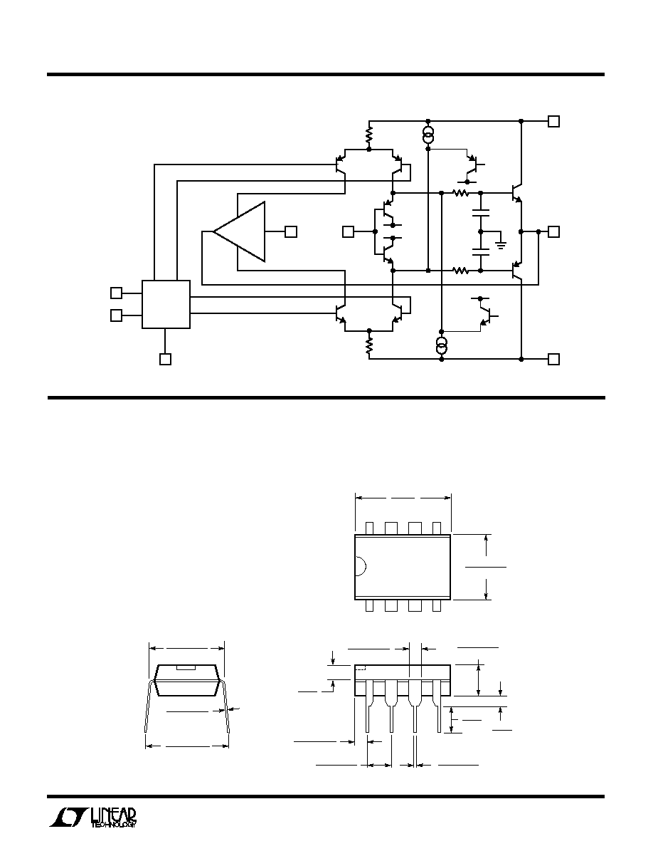
SI PLIFIED SCHE ATIC
W
W
Information furnished by Linear Technology Corporation is believed to be accurate and reliable.
However, no responsibility is assumed for its use. Linear Technology Corporation makes no represen-
tation that the interconnection of its circuits as described herein will not infringe on existing patent rights.
Dimensions in inches (millimeters) unless otherwise noted.
PACKAGE DESCRIPTIO
U
N8 Package
8-Lead Plastic DIP
N8 0392
0.045 ± 0.015
(1.143 ± 0.381)
0.100 ± 0.010
(2.540 ± 0.254)
0.065
(1.651)
TYP
0.045 ≠ 0.065
(1.143 ≠ 1.651)
0.130 ± 0.005
(3.302 ± 0.127)
0.020
(0.508)
MIN
0.018 ± 0.003
(0.457 ± 0.076)
0.125
(3.175)
MIN
1
2
3
4
8
7
6
5
0.250 ± 0.010
(6.350 ± 0.254)
0.400
(10.160)
MAX
0.009 ≠ 0.015
(0.229 ≠ 0.381)
0.300 ≠ 0.320
(7.620 ≠ 8.128)
0.325
+0.025
≠0.015
+0.635
≠0.381
8.255
(
)

16
LT1203/LT1205
PACKAGE DESCRIPTIO
U
Dimensions in inches (millimeters) unless otherwise noted.
S8 Package
8-Lead Plastic SOIC
1
2
3
4
0.150 ≠ 0.157*
(3.810 ≠ 3.988)
8
7
6
5
0.189 ≠ 0.197*
(4.801 ≠ 5.004)
0.228 ≠ 0.244
(5.791 ≠ 6.197)
0.016 ≠ 0.050
0.406 ≠ 1.270
0.010 ≠ 0.020
(0.254 ≠ 0.508)
◊
45
∞
0∞≠ 8∞ TYP
0.008 ≠ 0.010
(0.203 ≠ 0.254)
SO8 0294
0.053 ≠ 0.069
(1.346 ≠ 1.752)
0.014 ≠ 0.019
(0.355 ≠ 0.483)
0.004 ≠ 0.010
(0.101 ≠ 0.254)
0.050
(1.270)
BSC
*THESE DIMENSIONS DO NOT INCLUDE MOLD FLASH OR PROTRUSIONS.
MOLD FLASH OR PROTRUSIONS SHALL NOT EXCEED 0.006 INCH (0.15mm).
0.016 ≠ 0.050
0.406 ≠ 1.270
0.010 ≠ 0.020
(0.254 ≠ 0.508)
◊
45
∞
0∞ ≠ 8∞ TYP
0.008 ≠ 0.010
(0.203 ≠ 0.254)
1
2
3
4
5
6
7
8
0.150 ≠ 0.157*
(3.810 ≠ 3.988)
16
15
14
13
0.386 ≠ 0.394*
(9.804 ≠ 10.008)
0.228 ≠ 0.244
(5.791 ≠ 6.197)
12
11
10
9
SO16 0893
0.053 ≠ 0.069
(1.346 ≠ 1.752)
0.014 ≠ 0.019
(0.355 ≠ 0.483)
0.004 ≠ 0.010
(0.101 ≠ 0.254)
0.050
(1.270)
TYP
*THESE DIMENSIONS DO NOT INCLUDE MOLD FLASH OR PROTRUSIONS.
MOLD FLASH OR PROTRUSIONS SHALL NOT EXCEED 0.006 INCH (0.15mm).
S Package
16-Lead Plastic SOIC
©
LINEAR TECHNOLOGY CORPORATION 1994
LT/GP 0494 10K ∑ PRINTED IN USA
Linear Technology Corporation
1630 McCarthy Blvd., Milpitas, CA 95035-7487
(408) 432-1900
q
FAX
: (408) 434-0507
q
TELEX
: 499-3977