LTC2053
1
2053fa
FEATURES
DESCRIPTIO
U
APPLICATIO S
U
TYPICAL APPLICATIO
U
The LTC
Æ
2053 is a high precision instrumentation ampli-
fier. The CMRR is typically 116dB with a single or dual 5V
supply and is independent of gain. The input offset voltage
is guaranteed below 10
µ
V with a temperature drift of less
than 50nV/
∞
C. The LTC2053 is easy to use; the gain is
adjustable with two external resistors, like a traditional
op amp.
The LTC2053 uses charge balanced sampled data tech-
niques to convert a differential input voltage into a single
ended signal that is in turn amplified by a zero-drift
operational amplifier.
The differential inputs operate from rail-to-rail and the
single ended output swings from rail-to-rail. The LTC2053
can be used in single supply applications, as low as 2.7V.
It can also be used with dual
±
5.5V supplies. The LTC2053
is available in an MS8 surface mount package. For space
limited applications, the LTC2053 is available in a
3mm
◊
3mm
◊
0.8mm dual fine pitch leadless package
(DFN).
s
Thermocouple Amplifiers
s
Electronic Scales
s
Medical Instrumentation
s
Strain Gauge Amplifiers
s
High Resolution Data Acquisition
, LTC and LT are registered trademarks of Linear Technology Corporation.
s
116dB CMRR Independent of Gain
s
Maximum Offset Voltage: 10
µ
V
s
Maximum Offset Voltage Drift: 50nV/
∞
C
s
Rail-to-Rail Input
s
Rail-to-Rail Output
s
2-Resistor Programmable Gain
s
Supply Operation: 2.7V to
±
5.5V
s
Typical Noise: 2.5
µ
V
P-P
(0.01Hz to 10Hz)
s
Typical Supply Current: 750
µ
A
s
Available in an MS8 and 3mm
◊
3mm
◊
0.8mm
DFN Packages
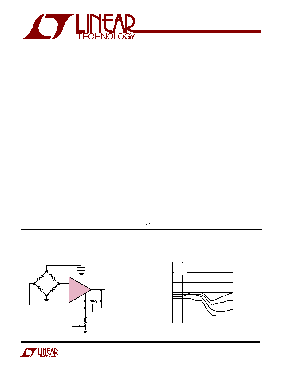
Precision, Rail-to-Rail
Input and Output, Zero-Drift Instrumentation
Amplifier with Resistor-Programmable Gain
+
≠
LTC2053
2
3
7
8
0.1
µ
F
3V
R < 10k
1, 4
5
6
R2 10k
2053 TA01
OUT
0.1
µ
F
R1
10
GAIN = 1+
R2
R1
Differential Bridge Amplifier
Typical Input Referred Offset vs Input
Common Mode Voltage (V
S
= 3V)
INPUT COMMON MODE VOLTAGE (V)
0
INPUT OFFSET VOLTAGE (
µ
V)
15
10
5
0
≠5
≠10
≠15
0.5
1.0
1.5
2.0
2053 G01
2.5
3.0
V
S
= 3V
V
REF
= 0V
T
A
= 25
∞
C
G = 1000
G = 100
G = 10
G = 1
LTC2053
2
2053fa
TOP VIEW
DD PACKAGE
8-LEAD (3mm
◊
3mm) PLASTIC DFN
5
6
7
8
4
3
2
1
EN
≠IN
+IN
V
≠
V
+
OUT
RG
REF
PACKAGE/ORDER I FOR ATIO
U
U
W
Total Supply Voltage (V
+
to V
≠
) ............................... 11V
Input Current ......................................................
±
10mA
V
IN
+
≠ V
REF
........................................................
5.5V
V
IN
≠
≠ V
REF
........................................................
5.5V
Output Short Circuit Duration .......................... Indefinite
ORDER PART NUMBER*
DD PART MARKING
T
JMAX
= 125
∞
C,
JA
= 160
∞
C/W
UNDERSIDE METAL INTERNALLY
CONNECTED TO V
≠
(PCB CONNECTION OPTIONAL)
LAEQ
LTC2053CDD
LTC2053IDD
LTC2053HDD
ABSOLUTE AXI U
RATI GS
W
W
W
U
(Note 1)
*The temperature grade (C, I, or H) of the LTC2053 in the DFN package is indicated on the shipping container.
Consult LTC Marketing for parts specified with wider operating temperature ranges.
ORDER PART NUMBER
MS8 PART MARKING
T
JMAX
= 150
∞
C,
JA
= 200
∞
C/W
LTVT
LTJY
LTAFB
LTC2053CMS8
LTC2053IMS8
LTC2053HMS8
1
2
3
4
EN
≠IN
+IN
V
≠
8
7
6
5
V
+
OUT
RG
REF
TOP VIEW
MS8 PACKAGE
8-LEAD PLASTIC MSOP
Operating Temperature Range
LTC2053C ............................................... 0
∞
C to 70
∞
C
LTC2053I ............................................ ≠ 40
∞
C to 85
∞
C
LTC2053H ........................................ ≠ 40
∞
C to 125
∞
C
Storage Temperature Range
MS8 Package ................................... ≠ 65
∞
C to 150
∞
C
DD Package ...................................... ≠ 65
∞
C to 125
∞
C
Lead Temperature (Soldering, 10 sec).................. 300
∞
C
ELECTRICAL CHARACTERISTICS
The
q
denotes the specifications which apply over the full operating
temperature range, otherwise specifications are at T
A
= 25
∞
C. V
+
= 3V, V
≠
= 0V, REF = 200mV. Output voltage swing is referenced
to V
≠
. All other specifications reference the OUT pin to the REF pin.
PARAMETER
CONDITIONS
MIN
TYP
MAX
UNITS
Gain Error
A
V
= 1
q
0.001
0.01
%
Gain Nonlinearity
A
V
= 1
q
3
12
ppm
Input Offset Voltage (Note 2)
V
CM
= 200mV
≠ 5
±
10
µ
V
Average Input Offset Drift (Note 2)
T
A
= ≠ 40
∞
C to 85
∞
C
q
±
50
nV/
∞
C
T
A
= 85
∞
C to 125
∞
C
q
≠1
≠2.5
µ
V/
∞
C
Average Input Bias Current (Note 3)
V
CM
= 1.2V
q
4
10
nA
Average Input Offset Current (Note 3)
V
CM
= 1.2V
q
1
3
nA
Input Noise Voltage
DC to 10Hz
2.5
µ
V
P-P
Common Mode Rejection Ratio
A
V
= 1, V
CM
= 0V to 3V, LTC2053C
q
105
113
dB
(Notes 4, 5)
A
V
= 1, V
CM
= 0.1V to 2.9V, LTC2053I
q
105
113
dB
A
V
= 1, V
CM
= 0V to 3V, LTC2053I
q
95
113
dB
A
V
= 1, V
CM
= 0.1V to 2.9V, LTC2053H
q
100
dB
A
V
= 1, V
CM
= 0V to 3V, LTC2053H
q
90
dB
LTC2053
3
2053fa
PARAMETER
CONDITIONS
MIN
TYP
MAX
UNITS
Power Supply Rejection Ratio (Note 6)
V
S
= 2.7V to 6V
q
110
116
dB
Output Voltage Swing High
R
L
= 2k to V
≠
q
2.85
2.94
V
R
L
= 10k to V
≠
q
2.95
2.98
V
Output Voltage Swing Low
q
20
mV
Supply Current
V
EN
0.5V, No Load
q
0.75
1
mA
Supply Current, Shutdown
V
EN
2.5V
10
µ
A
EN Pin Input Low Voltage, V
IL
0.5
V
EN Pin Input High Voltage, V
IH
2.5
V
EN Pin Input Current
V
EN
= V
≠
≠ 0.5
≠10
µ
A
Internal Op Amp Gain Bandwidth
200
kHz
Slew Rate
0.2
V/
µ
s
Internal Sampling Frequency
3
kHz
PARAMETER
CONDITIONS
MIN
TYP
MAX
UNITS
Gain Error
A
V
= 1
q
0.001
0.01
%
Gain Nonlinearity
A
V
= 1
q
3
10
ppm
Input Offset Voltage (Note 2)
V
CM
= 200mV
≠ 5
±
10
µ
V
Average Input Offset Drift (Note 2)
T
A
= ≠ 40
∞
C to 85
∞
C
q
±
50
nV/
∞
C
T
A
= 85
∞
C to 125
∞
C
q
≠1
≠2.5
µ
V/
∞
C
Average Input Bias Current (Note 3)
V
CM
= 1.2V
q
4
10
nA
Average Input Offset Current (Note 3)
V
CM
= 1.2V
q
1
3
nA
Common Mode Rejection Ratio
A
V
= 1, V
CM
= 0V to 5V, LTC2053C
q
105
116
dB
(Notes 4, 5)
A
V
= 1, V
CM
= 0.1V to 4.9V, LTC2053I
q
105
116
dB
A
V
= 1, V
CM
= 0V to 5V, LTC2053I
q
95
116
dB
A
V
= 1, V
CM
= 0.1V to 4.9V, LTC2053H
q
100
dB
A
V
= 1, V
CM
= 0V to 5V, LTC2053H
q
90
dB
Power Supply Rejection Ratio (Note 6)
V
S
= 2.7V to 6V
q
110
116
dB
Output Voltage Swing High
R
L
= 2k to V
≠
q
4.85
4.94
V
R
L
= 10k to V
≠
q
4.95
4.98
V
Output Voltage Swing Low
q
20
mV
Supply Current
V
EN
0.5V, No Load
q
0.85
1.1
mA
Supply Current, Shutdown
V
EN
4.5V
10
µ
A
EN Pin Input Low Voltage, V
IL
0.5
V
EN Pin Input High Voltage, V
IH
4.5
V
EN Pin Input Current
V
EN
= V
≠
≠1
≠10
µ
A
Internal Op Amp Gain Bandwidth
200
kHz
Slew Rate
0.2
V/
µ
s
Internal Sampling Frequency
3
kHz
ELECTRICAL CHARACTERISTICS
The
q
denotes the specifications which apply over the full operating temperature range, otherwise specifications are at T
A
= 25
∞
C. V
+
= 5V,
V
≠
= 0V, REF = 200mV. Output voltage swing is referenced to V
≠
. All other specifications reference the OUT pin to the REF pin.
The
q
denotes the specifications which apply over the full operating
temperature range, otherwise specifications are at T
A
= 25
∞
C. V
+
= 3V, V
≠
= 0V, REF = 200mV. Output voltage swing is referenced
to V
≠
. All other specifications reference the OUT pin to the REF pin.
LTC2053
4
2053fa
Note 1: Absolute Maximum Ratings are those values beyond which the life
of a device may be impaired.
Note 2: These parameters are guaranteed by design. Thermocouple effects
preclude measurement of these voltage levels in high speed automatic test
systems. V
OS
is measured to a limit determined by test equipment
capability.
Note 3: If the total source resistance is less than 10k, no DC errors result
from the input bias currents or the mismatch of the input bias currents or
the mismatch of the resistances connected to ≠IN and +IN.
Note 4: The CMRR with a voltage gain, A
V
, larger than 10 is 120dB (typ).
Note 5: At temperatures above 70
∞
C, the common mode rejection ratio
lowers when the common mode input voltage is within 100mV of the
supply rails.
Note 6: The power supply rejection ratio (PSRR) measurement accuracy
depends on the proximity of the power supply bypass capacitor to the
device under test. Because of this, the PSRR is 100% tested to relaxed
limits at final test. However, their values are guaranteed by design to meet
the data sheet limits.
Gain Error
A
V
= 1
q
0.001
0.01
%
Gain Nonlinearity
A
V
= 1
q
3
10
ppm
Input Offset Voltage (Note 2)
V
CM
= 0V
10
±
20
µ
V
Average Input Offset Drift (Note 2)
T
A
= ≠ 40
∞
C to 85
∞
C
q
±
50
nV/
∞
C
T
A
= 85
∞
C to 125
∞
C
q
≠1
≠2.5
µ
V/
∞
C
Average Input Bias Current (Note 3)
V
CM
= 1V
q
4
10
nA
Average Input Offset Current (Note 3)
V
CM
= 1V
q
1
3
nA
Common Mode Rejection Ratio
A
V
= 1, V
CM
= ≠ 5V to 5V, LTC2053C
q
105
118
dB
(Notes 4, 5)
A
V
= 1, V
CM
= ≠ 4.9V to 4.9V, LTC2053I
q
105
118
dB
A
V
= 1, V
CM
= ≠ 5V to 5V, LTC2053I
q
95
118
dB
A
V
= 1, V
CM
= ≠4.9V to 4.9V, LTC2053H
q
100
dB
A
V
= 1, V
CM
= ≠5V to 5V, LTC2053H
q
90
dB
Power Supply Rejection Ratio (Note 6)
V
S
= 2.7V to 11V
q
110
116
dB
Maximum Output Voltage Swing
R
L
= 2k to GND, LTC2053C, LTC2053I
q
±
4.5
±
4.8
V
R
L
= 10k to GND, LTC2053C, LTC2053I, LTC2053H
q
±
4.6
±
4.9
V
R
L
= 2k to GND, LTC2053H
q
±
4.4
±
4.8
V
Supply Current
V
EN
≠ 4.5V, No Load
q
0.95
1.3
mA
Supply Current, Shutdown
V
EN
4.5V
20
µ
A
EN Pin Input Low Voltage, V
IL
≠ 4.5
V
EN Pin Input High Voltage, V
IH
4.5
V
EN Pin Input Current
V
EN
= V
≠
≠3
≠ 20
µ
A
Internal Op Amp Gain Bandwidth
200
kHz
Slew Rate
0.2
V/
µ
s
Internal Sampling Frequency
3
kHz
The
q
denotes the specifications which apply over the full operating
temperature range, otherwise specifications are at T
A
= 25
∞
C. V
+
= 5V, V
≠
= ≠ 5V, REF = 0V.
PARAMETER
CONDITIONS
MIN
TYP
MAX
UNITS
ELECTRICAL CHARACTERISTICS
LTC2053
5
2053fa
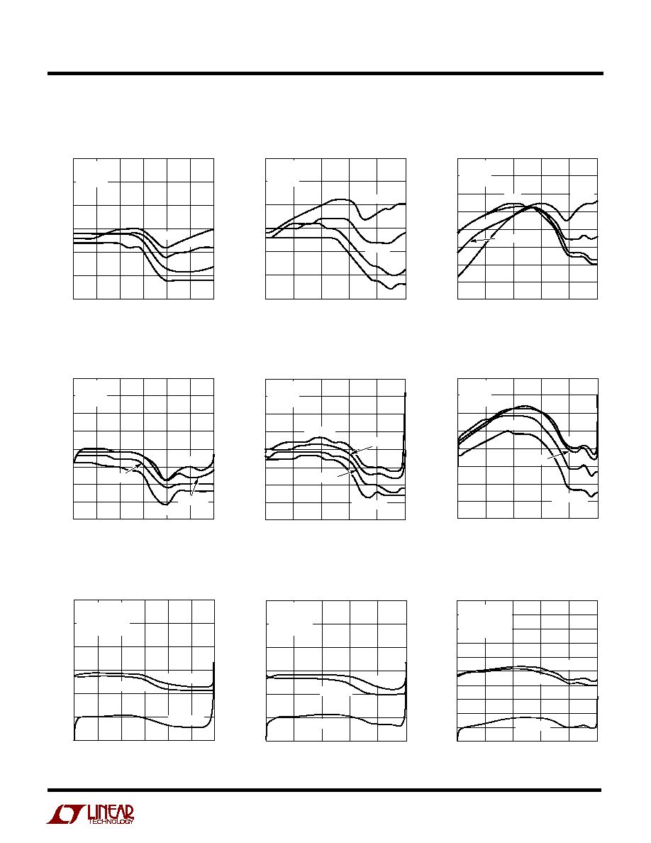
TYPICAL PERFOR A CE CHARACTERISTICS
U
W
Input Offset Voltage vs Input
Common Mode Voltage
Input Offset Voltage vs Input
Common Mode Voltage
Input Offset Voltage vs Input
Common Mode Voltage
Input Offset Voltage vs Input
Common Mode Voltage
Input Offset Voltage vs Input
Common Mode Voltage
Input Offset Voltage vs Input
Common Mode Voltage
Input Offset Voltage vs Input
Common Mode Voltage
Input Offset Voltage vs Input
Common Mode Voltage
Input Offset Voltage vs Input
Common Mode Voltage
INPUT COMMON MODE VOLTAGE (V)
0
INPUT OFFSET VOLTAGE (
µ
V)
15
10
5
0
≠5
≠10
≠15
0.5
1.0
1.5
2.0
2053 G01
2.5
3.0
V
S
= 3V
V
REF
= 0V
T
A
= 25
∞
C
G = 1000
G = 100
G = 10
G = 1
INPUT COMMON MODE VOLTAGE (V)
0
INPUT OFFSET VOLTAGE (
µ
V)
15
10
5
0
≠5
≠10
≠15
1
2
3
4
2053 G02
5
V
S
= 5V
V
REF
= 0V
T
A
= 25
∞
C
G = 1000
G = 100
G = 10
G = 1
INPUT COMMON MODE VOLTAGE (V)
≠5
INPUT OFFSET VOLTAGE (
µ
V)
20
15
10
5
0
≠5
≠10
≠15
≠20
≠3
≠1
1
3
2053 G03
5
V
S
=
±
5V
V
REF
= 0V
T
A
= 25
∞
C
G=1000
G=10
G=1
G=100
INPUT COMMON MODE VOLTAGE (V)
INPUT OFFSET VOLTAGE (
µ
V)
20
15
10
5
0
≠5
≠10
≠15
≠20
2053 G04
0
0.5
1.0
1.5
2.0
2.5
3.0
V
S
= 3V
V
REF
= 0V
G = 10
T
A
= 25
∞
C
T
A
= 85
∞
C
T
A
= 70
∞
C
T
A
= ≠55
∞
C
INPUT COMMON MODE VOLTAGE (V)
0
INPUT OFFSET VOLTAGE (
µ
V)
20
15
10
5
0
≠5
≠10
≠15
≠20
1
2
3
4
2053 G05
5
V
S
= 5V
V
REF
= 0V
G = 10
T
A
= 25
∞
C
T
A
= 85
∞
C
T
A
= ≠55
∞
C
T
A
= 70
∞
C
INPUT COMMON MODE VOLTAGE (V)
≠5
INPUT OFFSET VOLTAGE (
µ
V)
20
15
10
5
0
≠5
≠10
≠15
≠20
≠3
≠1
1
3
2053 G06
5
V
S
=
±
5V
V
REF
= 0V
G = 10
T
A
= 25
∞
C
T
A
= 85
∞
C
T
A
= ≠55
∞
C
T
A
= 70
∞
C
INPUT COMMON MODE VOLTAGE (V)
INPUT OFFSET VOLTAGE (
µ
V)
60
40
20
0
≠20
≠40
≠60
2053 G07
0
0.5
1.0
1.5
2.0
2.5
3.0
H-GRADE PARTS
V
S
= 3V
V
REF
= 0V
G = 10
T
A
= 25
∞
C
T
A
= 85
∞
C
T
A
= 125
∞
C
INPUT COMMON MODE VOLTAGE (V)
0
INPUT OFFSET VOLTAGE (
µ
V)
60
40
20
0
≠20
≠40
≠60
2053 G08
0
1
2
3
4
5
H-GRADE PARTS
V
S
= 5V
V
REF
= 0V
G = 10
T
A
= 25
∞
C
T
A
= 85
∞
C
T
A
= 125
∞
C
INPUT COMMON MODE VOLTAGE (V)
≠5
INPUT OFFSET VOLTAGE (
µ
V)
≠3
≠1
1
3
2053 G09
5
100
80
60
40
20
0
≠20
≠40
≠60
≠80
≠100
H-GRADE PARTS
V
S
=
±
5V
V
REF
= 0V
G = 10
T
A
= 25
∞
C
T
A
= 85
∞
C
T
A
= 125
∞
C