Electrical Specifications Subject to Change
Electrical Specifications Subject to Change
LTC2208
1
2208f
FEATURES
DESCRIPTIO
U
APPLICATIO S
U
TYPICAL APPLICATIO
U
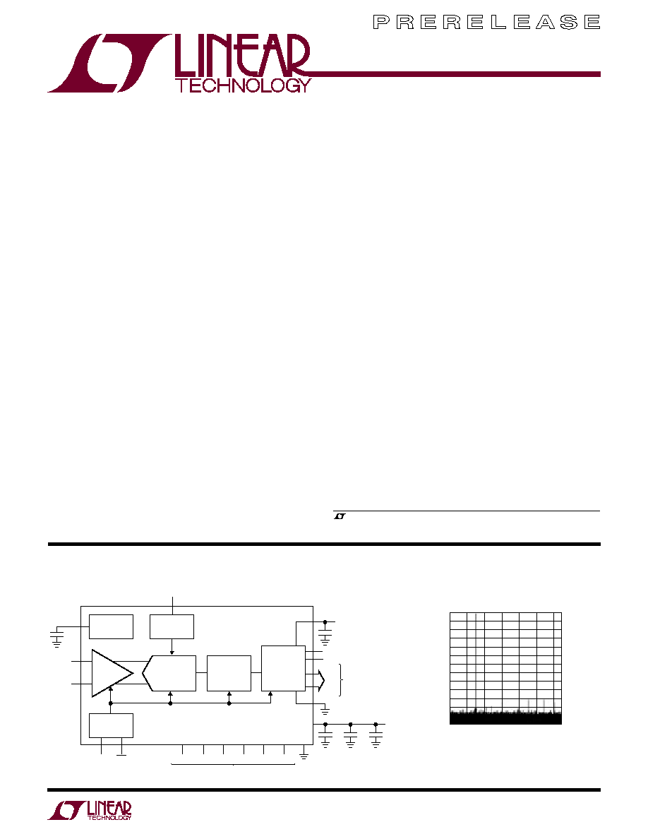
16-Bit, 130Msps ADC
The LTC
Æ
2208 is a 130Msps, sampling 16-bit A/D converter
designed for digitizing high frequency, wide dynamic range
signals up to input frequencies of 700MHz. The input range
of the ADC can be optimized with the PGA front end.
The LTC2208 is perfect for demanding communications
applications, with AC performance that includes 78dBFS
Noise Floor and 100dB spurious free dynamic range
(SFDR). Ultra low jitter of 70fs
RMS
allows undersampling
of high input frequencies with excellent noise performance.
Maximum DC specs include ±4LSB INL, ±1LSB DNL (no
missing codes) over temperature.
The digital output can be either differential LVDS or
single-ended CMOS. There are two format options for the
CMOS outputs: a single bus running at the full data rate or
demultiplexed buses running at half data rate. A separate
output power supply allows the CMOS output swing to
range from 0.5V to 3.3V.
The ENC
+
and ENC
≠
inputs may be driven differentially
or single-ended with a sine wave, PECL, LVDS, TTL or
CMOS inputs. An optional clock duty cycle stabilizer al-
lows high performance at full speed with a wide range of
clock duty cycle.
Telecommunications
Receivers
Cellular Base Stations
Spectrum Analysis
Imaging Systems
ATE
Sample Rate: 130Msps
78dBFS Noise Floor
100dB SFDR
SFDR >83dB at 250MHz (1.5V
P-P
Input Range)
PGA Front End (2.25V
P-P
or 1.5V
P-P
Input Range)
700MHz Full Power Bandwidth S/H
Optional Internal Dither
Optional Data Output Randomizer
LVDS or CMOS Outputs
Single 3.3V Supply
Power Dissipation: 1.25W
Clock Duty Cycle Stabilizer
Pin Compatible 14-Bit Version
130Msps: LTC2208 (16-Bit), LTC2208-14 (14-Bit)
64-Pin QFN Package
, LTC and LT are registered trademarks of Linear Technology Corporation.
All other trademarks are the property of their respective owners.
FREQUENCY (MHz)
0
≠130
AMPLITUDE (dBFS)
≠100
≠110
≠120
≠80
≠90
≠30
≠40
≠50
≠60
≠70
0
≠10
10
30
40
≠20
20
50
60
2208 G03
64k Point FFT, F
IN
= 15.1MHz,
≠1dB, PGA = 0
≠
+
S/H
AMP
CORRECTION
LOGIC AND
SHIFT REGISTER
OUTPUT
DRIVERS
16-BIT
PIPELINED
ADC CORE
INTERNAL ADC
REFERENCE
GENERATOR
1.25V
COMMON MODE
BIAS VOLTAGE
CLOCK/DUTY
CYCLE
CONTROL
D15
∑
∑
∑
D0
ENC
PGA
SHDN DITH MODE LVDS RAND
ENC
V
CM
ANALOG
INPUT
2208 TA01
CMOS
OR
LVDS
0.5V TO 3.3V
3.3V
3.3V
SENSE
OGND
OV
DD
2.2
µF
1
µF
1
µF
1
µF
1
µF
V
DD
GND
ADC CONTROL INPUTS
AIN
+
AIN
≠
OF
CLKOUT
LTC2208
2
2208f
ABSOLUTE AXI U RATI GS
W
W
W
U
FOR ATIO
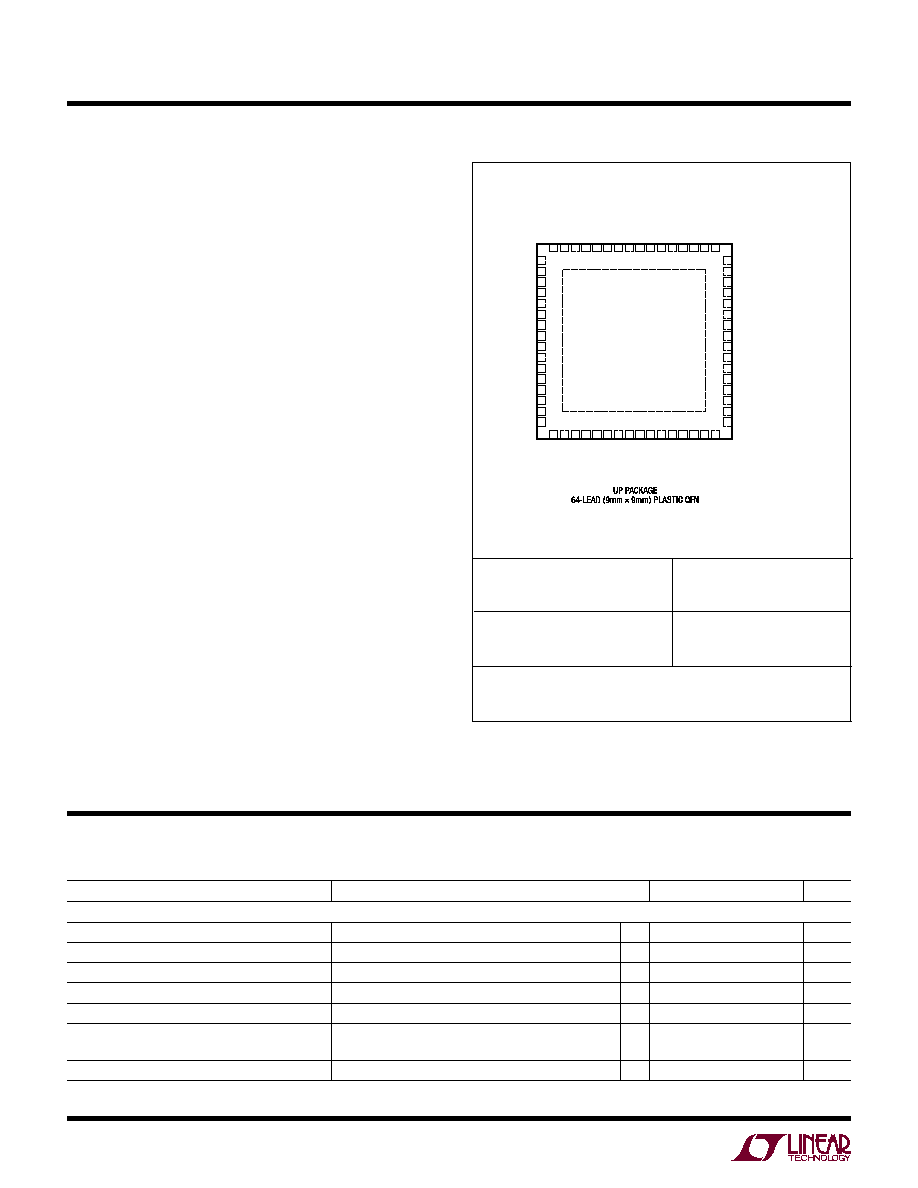
PACKAGE/ORDER I
U
U
W
CO VERTER CHARACTERISTICS
U
PARAMETER
CONDITIONS
MIN
TYP
MAX
UNITS
Resolution (No Missing Codes)
16
Bits
Integral Linearity Error
Differential Analog Input (Note 5)
±0.7
±4
LSB
Differential Linearity Error
Differential Analog Input
±0.3
±1
LSB
Offset Error
(Note 6)
±1
±5
mV
Offset Drift
±10
V/
∞C
Gain Error
External Reference
±0.2
±1.0
%FS
Full-Scale Drift
Internal Reference
±30
ppm/∞C
External Reference
±15
ppm/∞C
Transition Noise
2.9
LSB
RMS
Supply Voltage (V
DD
) ...................................≠0.3V to 4V
Digital Output Ground Voltage (OGND) ........≠0.3V to 1V
Analog Input Voltage (Note 3) ..... ≠0.3V to (V
DD
+ 0.3V)
Digital Input Voltage .................... ≠0.3V to (V
DD
+ 0.3V)
Digital Output Voltage ................≠0.3V to (OV
DD
+ 0.3V)
Power Dissipation ............................................ 2000mW
Operating Temperature Range
LTC2208C ................................................ 0∞C to 70∞C
LTC2208I .............................................≠40∞C to 85∞C
Storage Temperature Range ..................≠65∞C to 150∞C
Digital Output Supply Voltage (OV
DD
) ..........≠0.3V to 4V
ORDER PART
NUMBER
UP PART
MARKING*
EXPOSED PAD IS GND (PIN 65)
MUST BE SOLDERED TO PCB BOARD
T
JMAX
= 125∞C,
JA
= 20∞C/W
Consult LTC Marketing for parts specified with wider operating temperature ranges.
*The temperature grade is identified by a label on the shipping container.
LTC2208UP
LTC2208CUP
LTC2208IUP
OV
DD
= V
DD
(Notes 1 and 2)
The
denotes the specifications which apply over the full operating
temperature range, otherwise specifications are at T
A
= 25∞C. (Note 4)
TOP VIEW
65
SENSE
1
GND 2
V
CM
3
GND 4
V
DD
5
V
DD
6
GND 7
AIN
+
8
AIN
≠
9
GND 10
GND 11
ENC
+
12
ENC
≠
13
GND 14
V
DD
15
V
DD
16
48 D11
+
/DA6
47 D11
≠
/DA5
46 D10
+
/DA4
45 D10
≠
/DA3
44 D9
+
/DA2
43 D9
≠
/DA1
42 D8
+
/DA0
41 D8
≠
/CLKOUTA
40 CLKOUT
+
/CLKOUTB
39 CLKOUT
≠
/OFB
38 D7
+
/DB15
37 D7
≠
/DB14
36 D6
+
/DB13
35 D6
≠
/DB12
34 D5
+
/DB11
33 D5
≠
/DB10
64 PGA
63 RAND
62 MODE
61 L
VDS
60 OF
+
/OF
A
59 OF
≠
/DA15
58 D15
+
/DA14
57 D15
/DA13
56 D14
+
/DA12
55 D14
≠
≠
/DA11
54 D13
+
/DA10
53 D13
≠
≠
/DA9
52 D12
+
/DA8
51 D12
/DA7
50 OGND
49 OV
DD
V
DD
17
GND 18
SHDN
19
DITH
20
D0
≠
/DB0 21
DO
+
/DB1 22
D1
≠
/DB2 23
D1
+
/DB3 24
D2
≠
/DB4 25
D2
+
/DB5 26
D3
≠
/DB6 27
D3
+
/DB7 28
D4
≠
/DB8 29
D4
+
/DB9 30
OGND 31
OV
DD
32
Order Options Tape and Reel: Add #TR
Lead Free: Add #PBF Lead Free Tape and Reel: Add #TRPBF
Lead Free Part Marking:
http://www.linear.com/leadfree/
LTC2208
3
2208f
A ALOG I PUT
U
U
The
denotes the specifications which apply over the full operating temperature range, otherwise
specifications are at T
A
= 25∞C. (Note 4)
DY
A
IC ACCURACY
U
W
The
denotes the specifications which apply over the full operating temperature range,
otherwise specifications are at T
A
= 25∞C. A
IN
= ≠1dBFS. (Note 4)
SYMBOL
PARAMETER
CONDITIONS
MIN
TYP
MAX
UNITS
V
IN
Analog Input Range (A
IN
+
≠
A
IN
≠
)
3.135V V
DD
3.465V
1.5 to 2.25
V
P-P
V
IN, CM
Analog Input Common Mode
Differential Input (Note 7)
1
1.25
1.5
V
I
IN
Analog Input Leakage Current
0V A
IN
+
,
A
IN
≠
V
DD
≠1
1
µA
I
SENSE
SENSE Input Leakage Current
0V SENSE
V
DD
≠1
1
µA
I
MODE
MODE Pin Pull-Down Current to GND
10
µA
I
LVDS
LVDS Pin Pull-Down Current to GND
10
µA
C
IN
Analog Input Capacitance
Sample Mode ENC
+
< ENC
≠
6.5
pF
Hold Mode ENC
+
> ENC
≠
1.4
pF
t
AP
Sample-and-Hold
≠1.0
ns
Acquisition Delay Time
t
JITTER
Sample-and-Hold
50
fs RMS
Acquisition Delay Time Jitter
CMRR
Analog Input
1V < (A
IN
+
= A
IN
≠
) <1.5V
80
dB
Common Mode Rejection Ratio
BW-3dB
Full Power Bandwidth
R
S
< 20
700
MHz
SYMBOL
PARAMETER
CONDITIONS
MIN
TYP
MAX
UNITS
SNR
Signal-to-Noise Ratio
5MHz Input (2.25V Range, PGA = 0)
77.7
dBFS
5MHz Input (1.5V Range, PGA = 1)
75.3
dBFS
30MHz Input (2.25V Range, PGA = 0)
TBD
77.6
dBFS
30MHz Input (1.5V Range, PGA = 1)
75.2
dBFS
70MHz Input (2.25V Range, PGA = 0)
77.5
dBFS
70MHz Input (1.5V Range, PGA = 1)
75.1
dBFS
140MHz Input (2.25V Range, PGA = 0)
76.9
dBFS
140MHz Input (1.5V Range, PGA = 1)
74.8
dBFS
250MHz Input (2.25V Range, PGA = 0)
75.4
dBFS
250MHz Input (1.5V Range, PGA =1 )
TBD
73.8
dBFS
SFDR
Spurious Free
5MHz Input (2.25V Range, PGA = 0)
100
dB
Dynamic Range
5MHz Input (1.5V Range, PGA = 1)
100
dB
2
nd
or 3
rd
30MHz Input (2.25V Range, PGA = 0)
TBD
95
dB
Harmonic
30MHz Input (1.5V Range, PGA = 1)
100
dB
70MHz Input (2.25V Range, PGA = 0)
90
dB
70MHz Input (1.5V Range, PGA = 1)
95
dB
140MHz Input (2.25V Range, PGA = 0)
85
dB
140MHz Input (1.5V Range, PGA = 1)
TBD
90
dB
250MHz Input (2.25V Range, PGA = 0)
78
dB
250MHz Input (1.5V Range, PGA = 1)
83
dB
SFDR
Spurious Free
5MHz Input (2.25V Range, PGA = 0)
100
dB
Dynamic Range
5MHz Input (1.5V Range, PGA = 1)
100
dB
4
th
Harmonic
30MHz Input (2.25V Range, PGA = 0)
TBD
100
dB
or Higher
30MHz Input (1.5V Range, PGA = 1)
100
dB
70MHz Input (2.25V Range, PGA = 0)
100
dB
70MHz Input (1.5V Range, PGA = 1)
100
dB
140MHz Input (2.25V Range, PGA = 0)
95
dB
140MHz Input (1.5V Range, PGA = 1)
TBD
95
dB
250MHz Input (2.25V Range, PGA = 0)
90
dB
250MHz Input (1.5V Range, PGA = 1)
90
dB
LTC2208
4
2208f
PARAMETER
CONDITIONS
MIN
TYP
MAX
UNITS
V
CM
Output Voltage
I
OUT
= 0
1.15
1.25
1.35
V
V
CM
Output Tempco
I
OUT
= 0
±100
ppm/∞C
V
CM
Line Regulation
3.135V V
DD
3.465V
1
mV/ V
V
CM
Output Resistance
1mA | I
OUT
| 1mA
2
DY
A
IC ACCURACY
U
W
The
denotes the specifications which apply over the full operating temperature range,
otherwise specifications are at T
A
= 25∞C. A
IN
= ≠1dBFS unless otherwise noted. (Note 4)
The
denotes the specifications which apply over
the full operating temperature range, otherwise specifications are at T
A
= 25∞C. (Note 4)
SYMBOL
PARAMETER
CONDITIONS
MIN
TYP
MAX
UNITS
S/(N+D)
Signal-to-Noise
5MHz Input (2.25V Range, PGA = 0)
77.7
dBFS
Plus Distortion Ratio
5MHz Input (1.5V Range, PGA = 1)
75.3
dBFS
30MHz Input (2.25V Range, PGA = 0)
TBD
77.5
dBFS
30MHz Input (1.5V Range, PGA = 1)
75.2
dBFS
70MHz Input (2.25V Range, PGA = 0)
77.4
dBFS
70MHz Input (1.5V Range, PGA = 1)
75
dBFS
140MHz Input (2.25V Range, PGA = 0)
76.4
dBFS
140MHz Input (1.5V Range, PGA = 1)
TBD
74.5
dBFS
250MHz Input (2.25V Range, PGA = 0)
73.6
dBFS
250MHz Input (1.5V Range, PGA = 1)
72.9
dBFS
SFDR
Spurious Free
5MHz Input (2.25V Range, PGA = 0)
105
dBFS
at ≠25dBFS
5MHz Input (1.5V Range, PGA = 1)
105
dBFS
Dither "OFF"
30MHz Input (2.25V Range, PGA = 0)
TBD
105
dBFS
30MHz Input (1.5V Range, PGA = 1)
105
dBFS
70MHz Input (2.25V Range, PGA = 0)
105
dBFS
70MHz Input (1.5V Range, PGA = 1)
105
dBFS
140MHz Input (2.25V Range, PGA = 0)
100
dBFS
140MHz Input (1.5V Range, PGA = 1)
TBD
100
dBFS
250MHz Input (2.25V Range, PGA = 0)
100
dBFS
250MHz Input (1.5V Range, PGA = 1)
100
dBFS
SFDR
Spurious Free
5MHz Input (2.25V Range, PGA = 0)
115
dBFS
at ≠25dBFS
5MHz Input (1.5V Range, PGA = 1)
115
dBFS
Dither "ON"
30MHz Input (2.25V Range, PGA = 0)
TBD
115
dBFS
30MHz Input (1.5V Range, PGA = 1)
115
dBFS
70MHz Input (2.25V Range, PGA = 0)
115
dBFS
70MHz Input (1.5V Range, PGA = 1)
115
dBFS
140MHz Input (2.25V Range, PGA = 0)
110
dBFS
140MHz Input (1.5V Range, PGA = 1)
TBD
110
dBFS
250MHz Input (2.25V Range, PGA = 0)
105
dBFS
250MHz Input (1.5V Range, PGA = 1)
105
dBFS
LTC2208
5
2208f
The
denotes the specifications which apply over the
full operating temperature range, otherwise specifications are at T
A
= 25∞C. (Note 4)
DIGITAL I PUTS A D DIGITAL OUTPUTS
U
U
SYMBOL
PARAMETER
CONDITIONS
MIN
TYP
MAX
UNITS
ENCODE INPUTS (ENC
+
, ENC
≠
)
V
ID
Differential Input Voltage
0.2
V
V
ICM
Common Mode Input Voltage
Internally Set
1.6
V
Externally Set (Note 7)
TBD
V
R
IN
Input Resistance
(See Figure 2)
6
k
C
IN
Input Capacitance
(Note 7)
3
pF
LOGIC INPUTS (DITH, PGA, SHDN, RAND)
V
IH
High Level Input Voltage
V
DD
= 3.3V
2
V
V
IL
Low Level Input Voltage
V
DD
= 3.3V
0.8
V
I
IN
Digital Input Current
V
IN
= 0V to V
DD
±10
µA
C
IN
Digital Input Capacitance
(Note 7)
1.5
pF
LOGIC OUTPUTS (CMOS MODE)
OV
DD
= 3.3V
V
OH
High Level Output Voltage
V
DD
= 3.3V
I
O
= ≠10µA
3.299
V
I
O
= ≠200µA
3.1
3.29
V
V
OL
Low Level Output Voltage
V
DD
= 3.3V
I
O
= 160µA
0.01
V
I
O
= 1.6mA
0.10
0.4
V
I
SOURCE
Output Source Current
V
OUT
= 0V
≠50
mA
I
SINK
Output Sink Current
V
OUT
= 3.3V
50
mA
OV
DD
= 2.5V
V
OH
High Level Output Voltage
V
DD
= 3.3V
I
O
= ≠200µA
2.49
V
V
OL
Low Level Output Voltage
V
DD
= 3.3V
I
O
= 1.60mA
0.1
V
OV
DD
= 1.8V
V
OH
High Level Output Voltage
V
DD
= 3.3V
I
O
= ≠200µA
1.79
V
V
OL
Low Level Output Voltage
V
DD
= 3.3V
I
O
= 1.60mA
0.1
V
LOGIC OUTPUTS (LVDS MODE)
STANDARD LVDS
V
OD
Differential Ouptut Voltage
100 Differential Load
247
350
454
mV
V
OS
Output Common Mode Voltage
100 Differential Load
1.125
1.2
1.375
V
LOW POWER LVDS
V
OD
Differential Ouptut Voltage
100 Differential Load
150
200
250
mV
V
OS
Output Common Mode Voltage
100 Differential Load
1.125
1.2
1.375
V