2410.pm6
LTC2410
1
The LTC
®
2410 is a 2.7V to 5.5V micropower 24-bit
differential
analog to digital converter with an inte-
grated oscillator, 2ppm INL and 0.16ppm RMS noise. It
uses delta-sigma technology and provides single cycle
settling time for multiplexed applications. Through a
single pin, the LTC2410 can be configured for better than
110dB input differential mode rejection at 50Hz or 60Hz
±
2%, or it can be driven by an external oscillator for a user
defined rejection frequency. The internal oscillator re-
quires no external frequency setting components.
The converter accepts any external differential reference
voltage from 0.1V to V
CC
for flexible ratiometric and
remote sensing measurement configurations. The full-
scale differential input range is from 0.5V
REF
to 0.5V
REF
.
The reference common mode voltage, V
REFCM
, and the
input common mode voltage, V
INCM
, may be indepen-
dently set anywhere within the GND to V
CC
range of the
LTC2410. The DC common mode input rejection is better
than 140dB.
The LTC2410 communicates through a flexible 3-wire
digital interface which is compatible with SPI and
MICROWIRE
TM
protocols.
s
Direct Sensor Digitizer
s
Weight Scales
s
Direct Temperature Measurement
s
Gas Analyzers
s
Strain-Gage Transducers
s
Instrumentation
s
Data Acquisition
s
Industrial Process Control
s
6-Digit DVMs
, LTC and LT are registered trademarks of Linear Technology Corporation.
s
Differential Input and Differential Reference with
GND to V
CC
Common Mode Range
s
2ppm INL, No Missing Codes
s
2.5ppm Full-Scale Error
s
0.1ppm Offset
s
0.16ppm Noise
s
Single Conversion Settling Time for Multiplexed
Applications
s
Internal Oscillator--No External Components
Required
s
110dB Min, 50Hz or 60Hz Notch Filter
s
24-Bit ADC in Narrow SSOP-16 Package
(SO-8 Footprint)
s
Single Supply 2.7V to 5.5V Operation
s
Low Supply Current (200
µ
A) and Auto Shutdown
s
Fully Differential Version of LTC2400
24-Bit No Latency
TM
ADC
with Differential Input and
Differential Reference
No Latency
is a trademark of Linear Technology Corporation.
MICROWIRE is a trademark of National Semiconductor Corporation.
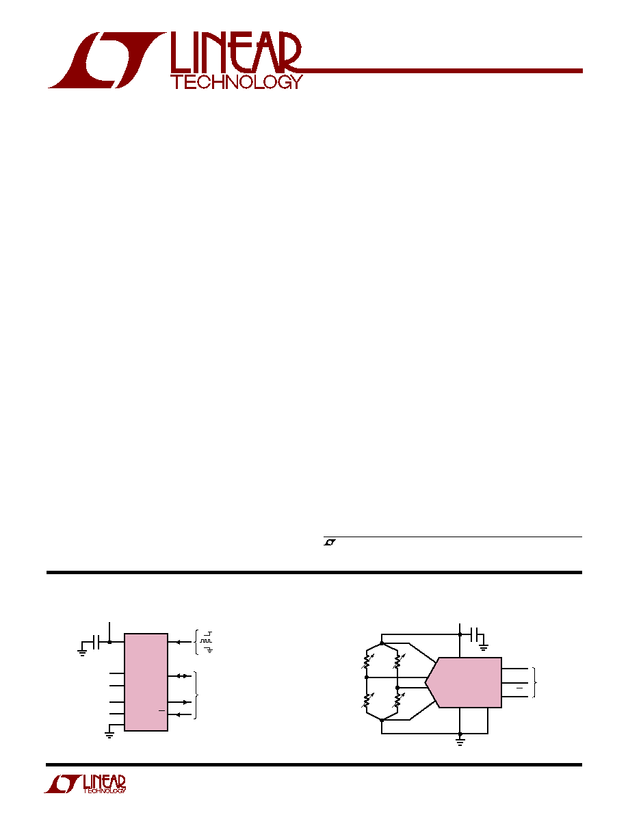
V
CC
F
O
REF
+
REF
SCK
IN
+
IN
SDO
GND
CS
2
14
3
4
13
5
6
12
1, 7, 8, 9, 10, 15, 16
11
REFERENCE
VOLTAGE
0.1V TO V
CC
ANALOG INPUT RANGE
0.5V
REF
TO 0.5V
REF
= INTERNAL OSC/50Hz REJECTION
= EXTERNAL CLOCK SOURCE
= INTERNAL OSC/60Hz REJECTION
3-WIRE
SPI INTERFACE
1
µ
F
2.7V TO 5.5V
LTC2410
2410 TA01
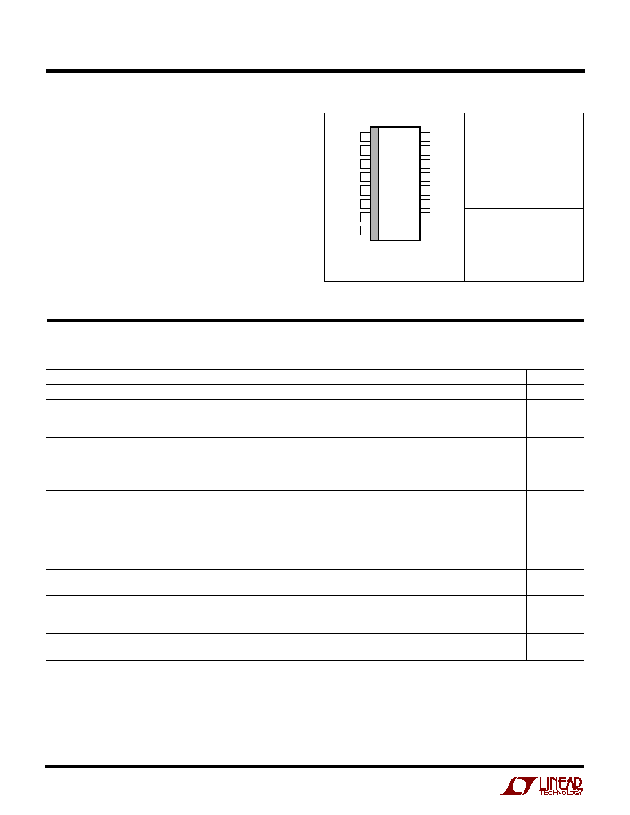
V
CC
LTC2410
IN
+
REF
+
V
CC
REF
V
CC
GND
F
O
IN
1
µ
F
SDO
3-WIRE
SPI INTERFACE
SCK
2410 TA02
CS
12
3
2
1, 7, 8
9, 10,
15, 16
14
5
6
4
13
11
BRIDGE
IMPEDANCE
100
TO 10k
APPLICATIO S
U
FEATURES
DESCRIPTIO
U
TYPICAL APPLICATIO S
U
LTC2410
2
ABSOLUTE AXI U
RATI GS
W
W
W
U
PACKAGE/ORDER I FOR ATIO
U
U
W
ELECTRICAL CHARACTERISTICS
(Notes 1, 2)
ORDER PART NUMBER
Consult factory for parts specified with wider operating temperature ranges.
Supply Voltage (V
CC
) to GND ....................... 0.3V to 7V
Analog Input Pins Voltage
to GND .................................... 0.3V to (V
CC
+ 0.3V)
Reference Input Pins Voltage
to GND .................................... 0.3V to (V
CC
+ 0.3V)
Digital Input Voltage to GND ........ 0.3V to (V
CC
+ 0.3V)
Digital Output Voltage to GND ..... 0.3V to (V
CC
+ 0.3V)
Operating Temperature Range
LTC2410C ............................................... 0
°
C to 70
°
C
LTC2410I ............................................ 40
°
C to 85
°
C
Storage Temperature Range ................. 65
°
C to 150
°
C
Lead Temperature (Soldering, 10 sec).................. 300
°
C
T
JMAX
= 125
°
C,
JA
= 110
°
C/W
LTC2410CGN
LTC2410IGN
PARAMETER
CONDITIONS
MIN
TYP
MAX
UNITS
Resolution (No Missing Codes)
0.1V
V
REF
V
CC
, 0.5 · V
REF
V
IN
0.5 · V
REF
, (Note 5)
q
24
Bits
Integral Nonlinearity
5V
V
CC
5.5V, REF
+
= 2.5V, REF
= GND, V
INCM
= 1.25V, (Note 6)
1
ppm of V
REF
5V
V
CC
5.5V, REF
+
= 5V, REF
= GND, V
INCM
= 2.5V, (Note 6)
q
2
14
ppm of V
REF
REF
+
= 2.5V, REF
= GND, V
INCM
= 1.25V, (Note 6)
5
ppm of V
REF
Offset Error
2.5V
REF
+
V
CC
, REF
= GND,
q
0.5
2.5
µ
V
GND
IN
+
= IN
V
CC
, (Note 14)
Offset Error Drift
2.5V
REF
+
V
CC
, REF
= GND,
10
nV/
°
C
GND
IN
+
= IN
V
CC
Positive Full-Scale Error
2.5V
REF
+
V
CC
, REF
= GND,
q
2.5
12
ppm of V
REF
IN
+
= 0.75REF
+
, IN
= 0.25 · REF
+
Positive Full-Scale Error Drift
2.5V
REF
+
V
CC
, REF
= GND,
0.03
ppm of V
REF
/
°
C
IN
+
= 0.75REF
+
, IN
= 0.25 · REF
+
Negative Full-Scale Error
2.5V
REF
+
V
CC
, REF
= GND,
q
2.5
12
ppm of V
REF
IN
+
= 0.25 · REF
+
, IN
= 0.75 · REF
+
Negative Full-Scale Error Drift
2.5V
REF
+
V
CC
, REF
= GND,
0.03
ppm of V
REF
/
°
C
IN
+
= 0.25 · REF
+
, IN
= 0.75 · REF
+
Total Unadjusted Error
5V
V
CC
5.5V, REF
+
= 2.5V, REF
= GND, V
INCM
= 1.25V
3
ppm of V
REF
5V
V
CC
5.5V, REF
+
= 5V, REF
= GND, V
INCM
= 2.5V
3
ppm of V
REF
REF
+
= 2.5V, REF
= GND, V
INCM
= 1.25V, (Note 6)
4
ppm of V
REF
Output Noise
5V
V
CC
5.5V, REF
+
= 5V, REF
= GND,
0.8
µ
V
RMS
GND
IN
= IN
+
V
CC
, (Note 13)
The
q
denotes specifications which apply over the full operating
temperature range, otherwise specifications are at T
A
= 25
°
C. (Notes 3, 4)
GN PART MARKING
2410
2410I
TOP VIEW
GN PACKAGE
16-LEAD PLASTIC SSOP
1
2
3
4
5
6
7
8
16
15
14
13
12
11
10
9
GND
V
CC
REF
+
REF
IN
+
IN
GND
GND
GND
GND
F
O
SCK
SDO
CS
GND
GND
LTC2410
3
SYMBOL
PARAMETER
CONDITIONS
MIN
TYP
MAX
UNITS
IN
+
Absolute/Common Mode IN
+
Voltage
q
GND 0.3V
V
CC
+ 0.3V
V
IN
Absolute/Common Mode IN
Voltage
q
GND 0.3V
V
CC
+ 0.3V
V
V
IN
Input Differential Voltage Range
q
V
REF
/2
V
REF
/2
V
(IN
+
IN
)
REF
+
Absolute/Common Mode REF
+
Voltage
q
0.1
V
CC
V
REF
Absolute/Common Mode REF
Voltage
q
GND
V
CC
0.1V
V
V
REF
Reference Differential Voltage Range
q
0.1
V
CC
V
(REF
+
REF
)
C
S
(IN
+
)
IN
+
Sampling Capacitance
18
pF
C
S
(IN
)
IN
Sampling Capacitance
18
pF
C
S
(REF
+
)
REF
+
Sampling Capacitance
18
pF
C
S
(REF
)
REF
Sampling Capacitance
18
pF
I
DC_LEAK
(IN
+
)
IN
+
DC Leakage Current
CS = V
CC
, IN
+
= GND
q
10
1
10
nA
I
DC_LEAK
(IN
)
IN
DC Leakage Current
CS = V
CC
, IN
= GND
q
10
1
10
nA
I
DC_LEAK
(REF
+
)
REF
+
DC Leakage Current
CS = V
CC
, REF
+
= 5V
q
10
1
10
nA
I
DC_LEAK
(REF
)
REF
DC Leakage Current
CS = V
CC
, REF
= GND
q
10
1
10
nA
The
q
denotes specifications which apply over the full operating
temperature range, otherwise specifications are at T
A
= 25
°
C. (Note 3)
The
q
denotes specifications which apply over the full operating
temperature range, otherwise specifications are at T
A
= 25
°
C. (Notes 3, 4)
PARAMETER
CONDITIONS
MIN
TYP
MAX
UNITS
Input Common Mode Rejection DC
2.5V
REF
+
V
CC
, REF
= GND,
q
130
140
dB
GND
IN
= IN
+
V
CC
Input Common Mode Rejection
2.5V
REF
+
V
CC
, REF
= GND,
q
140
dB
60Hz
±
2%
GND
IN
= IN
+
V
CC
, (Note 7)
Input Common Mode Rejection
2.5V
REF
+
V
CC
, REF
= GND,
q
140
dB
50Hz
±
2%
GND
IN
= IN
+
V
CC
, (Note 8)
Input Normal Mode Rejection
(Note 7)
q
110
140
dB
60Hz
±
2%
Input Normal Mode Rejection
(Note 8)
q
110
140
dB
50Hz
±
2%
Reference Common Mode
2.5V
REF
+
V
CC
, GND
REF
2.5V,
q
130
140
dB
Rejection DC
V
REF
= 2.5V, IN
= IN
+
= GND
Power Supply Rejection, DC
REF
+
= 2.5V, REF
= GND, IN
= IN
+
= GND
120
dB
Power Supply Rejection, 60Hz
±
2% REF
+
= 2.5V, REF
= GND, IN
= IN
+
= GND, (Note 7)
120
dB
Power Supply Rejection, 50Hz
±
2% REF
+
= 2.5V, REF
= GND, IN
= IN
+
= GND, (Note 8)
120
dB
CO VERTER CHARACTERISTICS
U
A ALOG I PUT A
U
D REFERE CE
U
U
U
LTC2410
4
SYMBOL
PARAMETER
CONDITIONS
MIN
TYP
MAX
UNITS
V
CC
Supply Voltage
q
2.7
5.5
V
I
CC
Supply Current
Conversion Mode
CS = 0V (Note 12)
q
200
300
µ
A
Sleep Mode
CS = V
CC
(Note 12)
q
20
30
µ
A
The
q
denotes specifications which apply over the full operating temperature range,
otherwise specifications are at T
A
= 25
°
C. (Note 3)
The
q
denotes specifications which apply over the full
operating temperature range, otherwise specifications are at T
A
= 25
°
C. (Note 3)
SYMBOL
PARAMETER
CONDITIONS
MIN
TYP
MAX
UNITS
V
IH
High Level Input Voltage
2.7V
V
CC
5.5V
q
2.5
V
CS, F
O
2.7V
V
CC
3.3V
2.0
V
V
IL
Low Level Input Voltage
4.5V
V
CC
5.5V
q
0.8
V
CS, F
O
2.7V
V
CC
5.5V
0.6
V
V
IH
High Level Input Voltage
2.7V
V
CC
5.5V (Note 9)
q
2.5
V
SCK
2.7V
V
CC
3.3V (Note 9)
2.0
V
V
IL
Low Level Input Voltage
4.5V
V
CC
5.5V (Note 9)
q
0.8
V
SCK
2.7V
V
CC
5.5V (Note 9)
0.6
V
I
IN
Digital Input Current
0V
V
IN
V
CC
q
10
10
µ
A
CS, F
O
I
IN
Digital Input Current
0V
V
IN
V
CC
(Note 9)
q
10
10
µ
A
SCK
C
IN
Digital Input Capacitance
10
pF
CS, F
O
C
IN
Digital Input Capacitance
(Note 9)
10
pF
SCK
V
OH
High Level Output Voltage
I
O
= 800
µ
A
q
V
CC
0.5V
V
SDO
V
OL
Low Level Output Voltage
I
O
= 1.6mA
q
0.4V
V
SDO
V
OH
High Level Output Voltage
I
O
= 800
µ
A (Note 10)
q
V
CC
0.5V
V
SCK
V
OL
Low Level Output Voltage
I
O
= 1.6mA (Note 10)
q
0.4V
V
SCK
I
OZ
Hi-Z Output Leakage
q
10
10
µ
A
SDO
DIGITAL I PUTS A D DIGITAL OUTPUTS
U
U
POWER REQUIRE E TS
W
U
LTC2410
5
Note 1: Absolute Maximum Ratings are those values beyond which the
life of the device may be impaired.
Note 2: All voltage values are with respect to GND.
Note 3: V
CC
= 2.7 to 5.5V unless otherwise specified.
V
REF
= REF
+
REF
, V
REFCM
= (REF
+
+ REF
)/2;
V
IN
= IN
+
IN
, V
INCM
= (IN
+
+ IN
)/2.
Note 4: F
O
pin tied to GND or to V
CC
or to external conversion clock
source with f
EOSC
= 153600Hz unless otherwise specified.
Note 5: Guaranteed by design, not subject to test.
Note 6: Integral nonlinearity is defined as the deviation of a code from
a straight line passing through the actual endpoints of the transfer
curve. The deviation is measured from the center of the quantization
band.
Note 7: F
O
= 0V (internal oscillator) or f
EOSC
= 153600Hz
±
2%
(external oscillator).
Note 8: F
O
= V
CC
(internal oscillator) or f
EOSC
= 128000Hz
±
2%
(external oscillator).
Note 9: The converter is in external SCK mode of operation such that
the SCK pin is used as digital input. The frequency of the clock signal
driving SCK during the data output is f
ESCK
and is expressed in kHz.
Note 10: The converter is in internal SCK mode of operation such that
the SCK pin is used as digital output. In this mode of operation the
SCK pin has a total equivalent load capacitance C
LOAD
= 20pF.
Note 11: The external oscillator is connected to the F
O
pin. The external
oscillator frequency, f
EOSC
, is expressed in kHz.
Note 12: The converter uses the internal oscillator.
F
O
= 0V or F
O
= V
CC
.
Note 13: The output noise includes the contribution of the internal
calibration operations.
Note 14: Guaranteed by design and test correlation.
SYMBOL
PARAMETER
CONDITIONS
MIN
TYP
MAX
UNITS
f
EOSC
External Oscillator Frequency Range
q
2.56
2000
kHz
t
HEO
External Oscillator High Period
q
0.25
390
µ
s
t
LEO
External Oscillator Low Period
q
0.25
390
µ
s
t
CONV
Conversion Time
F
O
= 0V
q
130.86
133.53
136.20
ms
F
O
= V
CC
q
157.03
160.23
163.44
ms
External Oscillator (Note 11)
q
20510/f
EOSC
(in kHz)
ms
f
ISCK
Internal SCK Frequency
Internal Oscillator (Note 10)
19.2
kHz
External Oscillator (Notes 10, 11)
f
EOSC
/8
kHz
D
ISCK
Internal SCK Duty Cycle
(Note 10)
q
45
55
%
f
ESCK
External SCK Frequency Range
(Note 9)
q
2000
kHz
t
LESCK
External SCK Low Period
(Note 9)
q
250
ns
t
HESCK
External SCK High Period
(Note 9)
q
250
ns
t
DOUT_ISCK
Internal SCK 32-Bit Data Output Time
Internal Oscillator (Notes 10, 12)
q
1.64
1.67
1.70
ms
External Oscillator (Notes 10, 11)
q
256/f
EOSC
(in kHz)
ms
t
DOUT_ESCK
External SCK 32-Bit Data Output Time
(Note 9)
q
32/f
ESCK
(in kHz)
ms
t
1
CS
to SDO Low Z
q
0
200
ns
t2
CS
to SDO High Z
q
0
200
ns
t3
CS
to SCK
(Note 10)
q
0
200
ns
t4
CS
to SCK
(Note 9)
q
50
ns
t
KQMAX
SCK
to SDO Valid
q
220
ns
t
KQMIN
SDO Hold After SCK
(Note 5)
q
15
ns
t
5
SCK Set-Up Before CS
q
50
ns
t
6
SCK Hold After CS
q
50
ns
The
q
denotes specifications which apply over the full operating temperature
range, otherwise specifications are at T
A
= 25
°
C. (Note 3)
TI I G CHARACTERISTICS
W
U