LTC2440
1
2440f
The LTC
Æ
2440 is a high speed 24-bit No Latency
TM
ADC
with 5ppm INL and 5
µ
V offset. It uses proprietary delta-
sigma architecture enabling variable speed and resolution
with no latency. Ten speed/resolution combinations (6.9Hz/
200nV
RMS
to 3.5kHz/25
µ
V
RMS
) are programmed through
a simple serial interface. Alternatively, by tying a single pin
HIGH or LOW, a fast (880Hz/2
µ
V
RMS
) or ultralow noise
(6.9Hz, 200nV
RMS
, 50/60Hz rejection) speed/resolution
combination can be easily selected. The accuracy (offset,
full-scale, linearity, drift) and power dissipation are inde-
pendent of the speed selected. Since there is no latency,
a speed/resolution change may be made between conver-
sions with no degradation in performance.
Following each conversion cycle, the LTC2440 automati-
cally enters a low power sleep state. Power dissipation
may be reduced by increasing the duration of this sleep
state. For example, running at the 3.5kHz conversion
speed but reading data at a 100Hz rate draws 240
µ
A
average current (1.1mW) while reading data at 7Hz output
rate draws only 25
µ
A (125
µ
W).
The LTC2440 communicates through a flexible 3- or
4-wire digital interface that is compatible with the LTC2410.
s
High Speed Multiplexing
s
Weight Scales
s
Auto Ranging 6-Digit DVMs
s
Direct Temperature Measurement
s
High Speed Data Acquisition
, LTC and LT are registered trademarks of Linear Technology Corporation.
s
Up to 3.5kHz Output Rate
s
Selectable Speed/Resolution
s
2
µ
V
RMS
Noise at 880Hz Output Rate
s
200nV
RMS
Noise at 6.9Hz Output Rate with
Simultaneous 50/60Hz Rejection
s
0.0005% INL, No Missing Codes
s
Autosleep Enables 20
µ
A Operation at 6.9Hz
s
< 5
µ
V Offset (4.5V < V
CC
< 5.5V, ≠ 40
∞
C to 85
∞
C)
s
Differential Input and Differential Reference with
GND to V
CC
Common Mode Range
s
No Latency, Each Conversion is Accurate Even After
an Input Step
s
Internal Oscillator--No External Components
s
24-Bit ADC in Narrow 16-Lead SSOP Package
s
Pin Compatible with the LTC2410
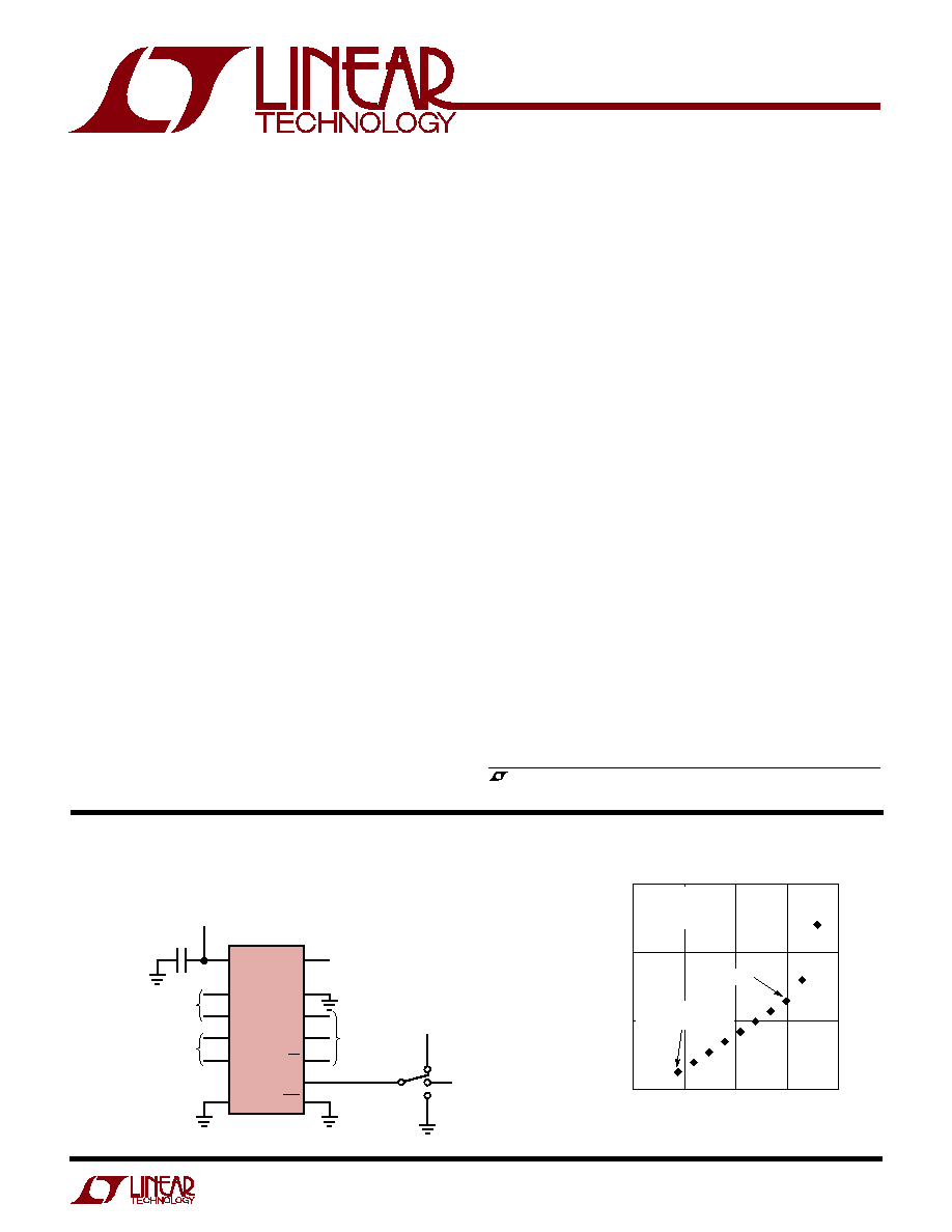
24-Bit High Speed
Differential
ADC with
Selectable Speed/Resolution
Speed vs RMS Noise
Simple 24-Bit 2-Speed Acquisition System
2
15
3
13
12
5
6
11
10
2440 TA01
2440 TA01
14
7
1, 8, 9, 16
REFERENCE VOLTAGE
0.1V TO V
CC
ANALOG INPUT
≠0.5V
REF
TO 0.5V
REF
3-WIRE
SPI INTERFACE
6.9Hz, 200nV NOISE,
50/60Hz REJECTION
880Hz OUTPUT RATE,
2
µ
V NOISE
10-SPEED SERIAL
PROGRAMMABLE
V
CC
4.5V TO 5.5V
4
V
CC
BUSY
F
O
REF
+
SCK
IN
+
IN
≠
SDO
GND
CS
EXT
SDI
LTC2440
REF
≠
CONVERSION RATE (Hz)
1
0.1
RMS NOISE (
µ
V)
1
10
100
10
100
2440 TA02
1000
10000
V
CC
= 5V
V
REF
= 5V
V
IN
+
= V
IN
≠
= 0V
2
µ
V AT 880Hz
200nV AT 6.9Hz
(50/60Hz REJECTION)
APPLICATIO S
U
FEATURES
TYPICAL APPLICATIO
U
DESCRIPTIO
U
No Latency
is a trademark of Linear Technology Corporation.
LTC2440
2
2440f
ABSOLUTE AXI U
RATI GS
W
W
W
U
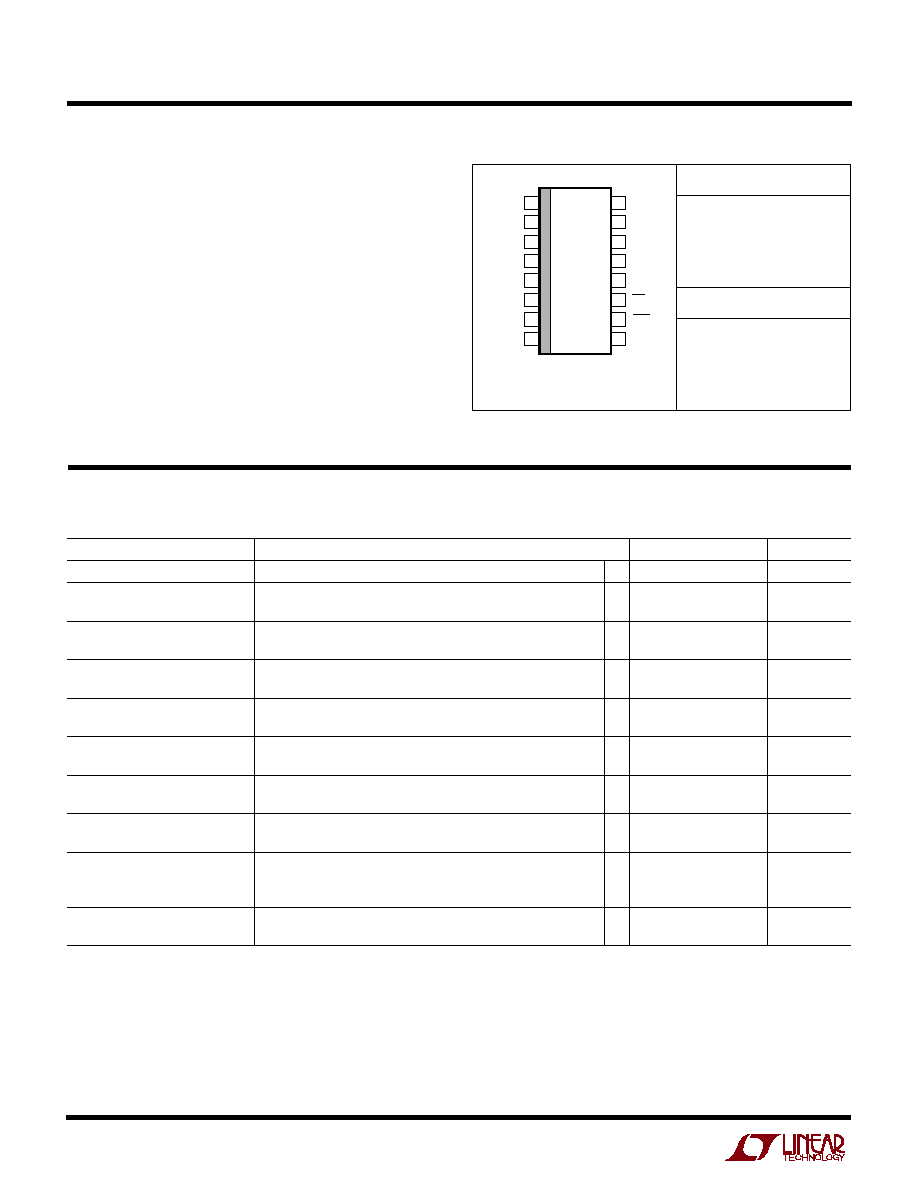
PACKAGE/ORDER I FOR ATIO
U
U
W
ELECTRICAL CHARACTERISTICS
(Notes 1, 2)
ORDER PART NUMBER
Supply Voltage (V
CC
) to GND .......................≠ 0.3V to 7V
Analog Input Pins Voltage
to GND .................................... ≠ 0.3V to (V
CC
+ 0.3V)
Reference Input Pins Voltage
to GND .................................... ≠ 0.3V to (V
CC
+ 0.3V)
Digital Input Voltage to GND ........ ≠ 0.3V to (V
CC
+ 0.3V)
Digital Output Voltage to GND ..... ≠ 0.3V to (V
CC
+ 0.3V)
Operating Temperature Range
LTC2440C ............................................... 0
∞
C to 70
∞
C
LTC2440I ............................................ ≠ 40
∞
C to 85
∞
C
Storage Temperature Range ................. ≠ 65
∞
C to 150
∞
C
Lead Temperature (Soldering, 10 sec).................. 300
∞
C
T
JMAX
= 125
∞
C,
JA
= 110
∞
C/W
LTC2440CGN
LTC2440IGN
PARAMETER
CONDITIONS
MIN
TYP
MAX
UNITS
Resolution (No Missing Codes)
0.1V
V
REF
V
CC
, ≠0.5 ∑ V
REF
V
IN
0.5 ∑ V
REF
, (Note 5)
q
24
Bits
Integral Nonlinearity
V
CC
= 5V, REF
+
= 5V, REF
≠
= GND, V
INCM
= 2.5V, (Note 6)
q
5
15
ppm of V
REF
REF
+
= 2.5V, REF
≠
= GND, V
INCM
= 1.25V, (Note 6)
3
ppm of V
REF
Offset Error
2.5V
REF
+
V
CC
, REF
≠
= GND,
q
2.5
5
µ
V
GND
IN
+
= IN
≠
V
CC
(Note 12)
Offset Error Drift
2.5V
REF
+
V
CC
, REF
≠
= GND,
20
nV/
∞
C
GND
IN
+
= IN
≠
V
CC
Positive Full-Scale Error
REF
+
= 5V, REF
≠
= GND, IN
+
= 3.75V, IN
≠
= 1.25V
q
10
30
ppm of V
REF
REF
+
= 2.5V, REF
≠
= GND, IN
+
= 1.875V, IN
≠
= 0.625V
q
10
50
ppm of V
REF
Positive Full-Scale Error Drift
2.5V
REF
+
V
CC
, REF
≠
= GND,
0.2
ppm of V
REF
/
∞
C
IN
+
= 0.75REF
+
, IN
≠
= 0.25 ∑ REF
+
Negative Full-Scale Error
REF
+
= 5V, REF
≠
= GND, IN
+
= 1.25V, IN
≠
= 3.75V
q
10
30
ppm of V
REF
REF
+
= 2.5V, REF
≠
= GND, IN
+
= 0.625V, IN
≠
= 1.875V
q
10
50
ppm of V
REF
Negative Full-Scale Error Drift
2.5V
REF
+
V
CC
, REF
≠
= GND,
0.2
ppm of V
REF
/
∞
C
IN
+
= 0.25 ∑ REF
+
, IN
≠
= 0.75 ∑ REF
+
Total Unadjusted Error
5V
V
CC
5.5V, REF
+
= 2.5V, REF
≠
= GND, V
INCM
= 1.25V
15
ppm of V
REF
5V
V
CC
5.5V, REF
+
= 5V, REF
≠
= GND, V
INCM
= 2.5V
15
ppm of V
REF
REF
+
= 2.5V, REF
≠
= GND, V
INCM
= 1.25V, (Note 6)
15
ppm of V
REF
Input Common Mode Rejection DC
2.5V
REF
+
V
CC
, REF
≠
= GND,
120
dB
GND
IN
≠
= IN
+
V
CC
The
q
denotes specifications which apply over the full operating
temperature range, otherwise specifications are at T
A
= 25
∞
C. (Notes 3, 4)
GN PART MARKING
2440
2440I
TOP VIEW
GN PACKAGE
16-LEAD PLASTIC SSOP
1
2
3
4
5
6
7
8
16
15
14
13
12
11
10
9
GND
V
CC
REF
+
REF
≠
IN
+
IN
≠
SDI
GND
GND
BUSY
F
O
SCK
SDO
CS
EXT
GND
Consult LTC Marketing for parts specified with wider operating temperature ranges.
LTC2440
3
2440f
SYMBOL
PARAMETER
CONDITIONS
MIN
TYP
MAX
UNITS
IN
+
Absolute/Common Mode IN
+
Voltage
q
GND ≠ 0.3V
V
CC
+ 0.3V
V
IN
≠
Absolute/Common Mode IN
≠
Voltage
q
GND ≠ 0.3V
V
CC
+ 0.3V
V
V
IN
Input Differential Voltage Range
q
≠V
REF
/2
V
REF
/2
V
(IN
+
≠ IN
≠
)
REF
+
Absolute/Common Mode REF
+
Voltage
q
0.1
V
CC
V
REF
≠
Absolute/Common Mode REF
≠
Voltage
q
GND
V
CC
≠ 0.1V
V
V
REF
Reference Differential Voltage Range
q
0.1
V
CC
V
(REF
+
≠ REF
≠
)
C
S
(IN
+
)
IN
+
Sampling Capacitance
5
pF
C
S
(IN
≠
)
IN
≠
Sampling Capacitance
5
pF
C
S
(REF
+
)
REF
+
Sampling Capacitance
5
pF
C
S
(REF
≠
)
REF
≠
Sampling Capacitance
5
pF
I
DC_LEAK
(IN
+
)
IN
+
DC Leakage Current
CS = V
CC
, IN
+
= GND
q
≠100
10
100
nA
I
DC_LEAK
(IN
≠
)
IN
≠
DC Leakage Current
CS = V
CC
, IN
≠
= GND
q
≠100
10
100
nA
I
DC_LEAK
(REF
+
)
REF
+
DC Leakage Current
CS = V
CC
, REF
+
= 5V
q
≠100
10
100
nA
I
DC_LEAK
(REF
≠
)
REF
≠
DC Leakage Current
CS = V
CC
, REF
≠
= GND
q
≠100
10
100
nA
The
q
denotes specifications which apply over the full operating
temperature range, otherwise specifications are at T
A
= 25
∞
C. (Note 3)
A ALOG I PUT A
U
D REFERE CE
U
U
U
The
q
denotes specifications which apply over the full
operating temperature range, otherwise specifications are at T
A
= 25
∞
C. (Note 3)
SYMBOL
PARAMETER
CONDITIONS
MIN
TYP
MAX
UNITS
V
IH
High Level Input Voltage
4.5V
V
CC
5.5V
q
2.5
V
CS, F
O
V
IL
Low Level Input Voltage
4.5V
V
CC
5.5V
q
0.8
V
CS, F
O
V
IH
High Level Input Voltage
4.5V
V
CC
5.5V (Note 8)
q
2.5
V
SCK
V
IL
Low Level Input Voltage
4.5V
V
CC
5.5V (Note 8)
q
0.8
V
SCK
I
IN
Digital Input Current
0V
V
IN
V
CC
q
≠10
10
µ
A
CS, F
O
I
IN
Digital Input Current
0V
V
IN
V
CC
(Note 8)
q
≠10
10
µ
A
SCK
C
IN
Digital Input Capacitance
10
pF
CS, F
O
C
IN
Digital Input Capacitance
(Note 8)
10
pF
SCK
V
OH
High Level Output Voltage
I
O
= ≠800
µ
A
q
V
CC
≠ 0.5V
V
SDO, BUSY
V
OL
Low Level Output Voltage
I
O
= 1.6mA
q
0.4V
V
SDO, BUSY
V
OH
High Level Output Voltage
I
O
= ≠800
µ
A (Note 9)
q
V
CC
≠ 0.5V
V
SCK
V
OL
Low Level Output Voltage
I
O
= 1.6mA (Note 9)
q
0.4V
V
SCK
I
OZ
Hi-Z Output Leakage
q
≠10
10
µ
A
SDO
DIGITAL I PUTS A D DIGITAL OUTPUTS
U
U
LTC2440
4
2440f
SYMBOL
PARAMETER
CONDITIONS
MIN
TYP
MAX
UNITS
V
CC
Supply Voltage
q
4.5
5.5
V
I
CC
Supply Current
Conversion Mode
CS = 0V (Note 7)
q
8
11
mA
Sleep Mode
CS = V
CC
(Note 7)
q
8
30
µ
A
The
q
denotes specifications which apply over the full operating temperature range,
otherwise specifications are at T
A
= 25
∞
C. (Note 3)
POWER REQUIRE E TS
W
U
SYMBOL
PARAMETER
CONDITIONS
MIN
TYP
MAX
UNITS
f
EOSC
External Oscillator Frequency Range
q
0.1
20
MHz
t
HEO
External Oscillator High Period
q
25
10000
ns
t
LEO
External Oscillator Low Period
q
25
10000
ns
t
CONV
Conversion Time
OSR = 256 (SDI = 0)
q
0.99
1.13
1.33
ms
OSR = 32768 (SDI = 1)
q
126
145
170
ms
External Oscillator (Note 10)
q
40000 ∑ OSR
f
EOSC
ms
f
ISCK
Internal SCK Frequency
Internal Oscillator (Note 9)
q
0.8
0.9
1
MHz
External Oscillator (Notes 9, 10)
f
EOSC
/10
Hz
D
ISCK
Internal SCK Duty Cycle
(Note 9)
q
45
55
%
f
ESCK
External SCK Frequency Range
(Note 8)
q
20
MHz
t
LESCK
External SCK Low Period
(Note 8)
q
25
ns
t
HESCK
External SCK High Period
(Note 8)
q
25
ns
t
DOUT_ISCK
Internal SCK 32-Bit Data Output Time
Internal Oscillator (Notes 9, 11)
q
41.6
35.3
30.9
µ
s
External Oscillator (Notes 9, 10)
q
320/f
EOSC
s
t
DOUT_ESCK
External SCK 32-Bit Data Output Time
(Note 8)
q
32/f
ESCK
s
t
1
CS
to SDO Low Z
q
0
200
ns
t
2
CS
to SDO High Z
q
0
200
ns
t
3
CS
to SCK
(Note 9)
5
µ
s
t
4
CS
to SCK
(Note 8)
5
µ
s
t
KQMAX
SCK
to SDO Valid
q
200
ns
t
KQMIN
SDO Hold After SCK
(Note 5)
q
15
ns
t
5
SCK Set-Up Before CS
q
50
ns
t
6
SCK Hold After CS
q
50
ns
t
7
SDI Setup Before SCK
q
10
Note 5
ns
t
8
SDI Hold After SCK
q
10
Note 5
ns
The
q
denotes specifications which apply over the full operating temperature
range, otherwise specifications are at T
A
= 25
∞
C. (Note 3)
TI I G CHARACTERISTICS
W
U
Note 1: Absolute Maximum Ratings are those values beyond which the life
of the device may be impaired.
Note 2: All voltage values are with respect to GND.
Note 3: V
CC
= 4.5 to 5.5V unless otherwise specified.
V
REF
= REF
+
≠ REF
≠
, V
REFCM
= (REF
+
+ REF
≠
)/2;
V
IN
= IN
+
≠ IN
≠
, V
INCM
= (IN
+
+ IN
≠
)/2.
Note 4: F
O
pin tied to GND or to external conversion clock source with
f
EOSC
= 10MHz unless otherwise specified.
Note 5: Guaranteed by design, not subject to test.
Note 6: Integral nonlinearity is defined as the deviation of a code from a
straight line passing through the actual endpoints of the transfer curve.
The deviation is measured from the center of the quantization band.
Note 7: The converter uses the internal oscillator.
Note 8: The converter is in external SCK mode of operation such that the
SCK pin is used as a digital input. The frequency of the clock signal driving
SCK during the data output is f
ESCK
and is expressed in Hz.
Note 9: The converter is in internal SCK mode of operation such that the
SCK pin is used as a digital output. In this mode of operation, the SCK pin
has a total equivalent load capacitance of C
LOAD
= 20pF.
Note 10: The external oscillator is connected to the F
O
pin. The external
oscillator frequency, f
EOSC
, is expressed in Hz.
Note 11: The converter uses the internal oscillator. F
O
= 0V.
Note 12: Guaranteed by design and test correlation.
LTC2440
5
2440f
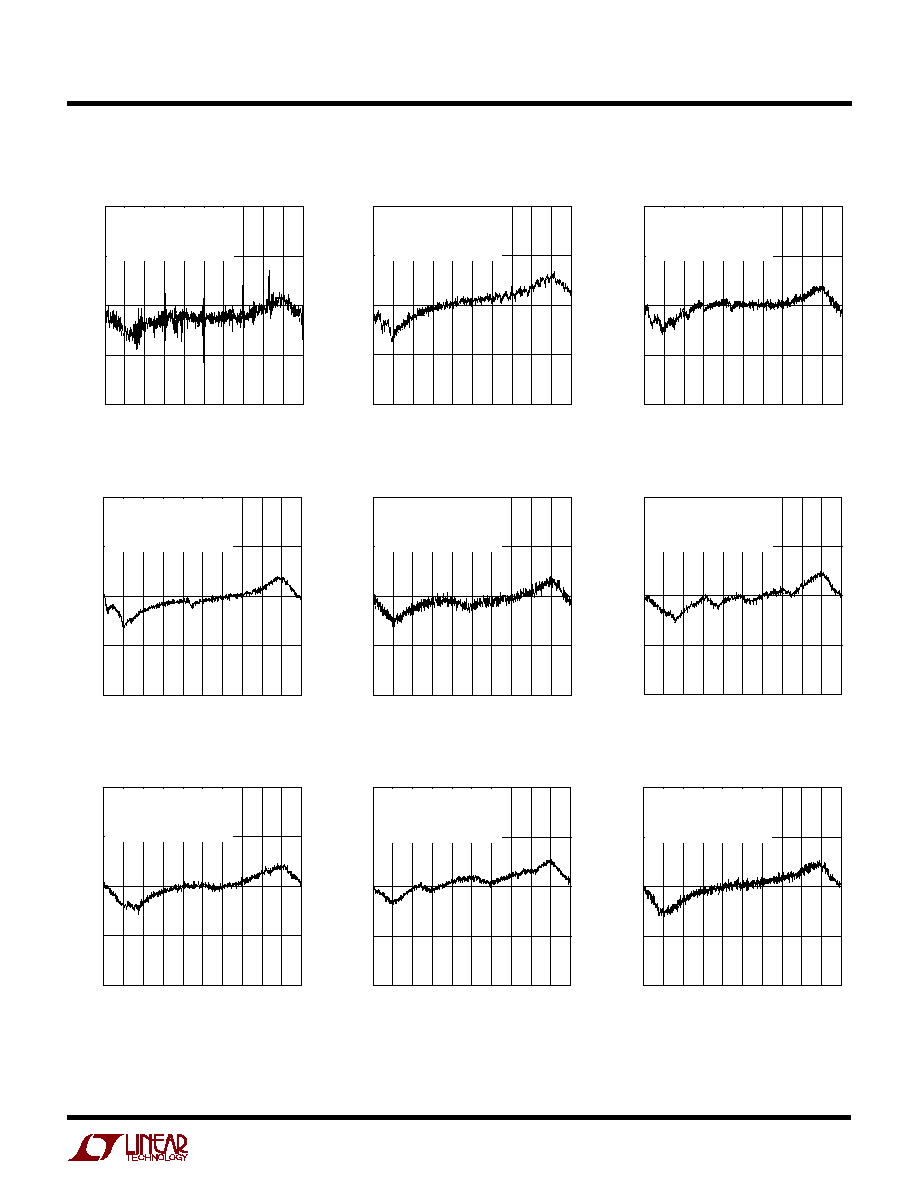
TYPICAL PERFOR A CE CHARACTERISTICS
U
W
Integral Nonlinearity f
OUT
= 3.5kHz
V
IN
(V)
≠2.5
INL ERROR (ppm OF V
REF
)
0
5
1.5
2440 G01
≠5
≠10
≠1.5
≠0.5 0
2.5
10
0.5
≠2
≠1
2
1
V
CC
= 5V
V
REF
= 5V
V
REF
+
= 5V
V
REF
≠
= GND
V
INCM
= 2.5V
F
O
= GND
T
A
= 25
∞
C
V
IN
(V)
≠2.5
INL ERROR (ppm OF V
REF
)
0
5
1.5
2440 G02
≠5
≠10
≠1.5
≠0.5 0
2.5
10
0.5
≠2
≠1
2
1
V
CC
= 5V
V
REF
= 5V
V
REF
+
= 5V
V
REF
≠
= GND
V
INCM
= 2.5V
F
O
= GND
T
A
= 25
∞
C
V
IN
(V)
≠2.5
INL ERROR (ppm OF V
REF
)
0
5
1.5
2440 G03
≠5
≠10
≠1.5
≠0.5 0
2.5
10
0.5
≠2
≠1
2
1
V
CC
= 5V
V
REF
= 5V
V
REF
+
= 5V
V
REF
≠
= GND
V
INCM
= 2.5V
F
O
= GND
T
A
= 25
∞
C
V
IN
(V)
≠2.5
INL ERROR (ppm OF V
REF
)
0
5
1.5
2440 G04
≠5
≠10
≠1.5
≠0.5 0
2.5
10
0.5
≠2
≠1
2
1
V
CC
= 5V
V
REF
= 5V
V
REF
+
= 5V
V
REF
≠
= GND
V
INCM
= 2.5V
F
O
= GND
T
A
= 25
∞
C
V
IN
(V)
≠2.5
INL ERROR (ppm OF V
REF
)
0
5
1.5
2440 G05
≠5
≠10
≠1.5
≠0.5 0
2.5
10
0.5
≠2
≠1
2
1
V
CC
= 5V
V
REF
= 5V
V
REF
+
= 5V
V
REF
≠
= GND
V
INCM
= 2.5V
F
O
= GND
T
A
= 25
∞
C
V
IN
(V)
≠2.5
INL ERROR (ppm OF V
REF
)
0
5
1.5
2440 G06
≠5
≠10
≠1.5
≠0.5 0
2.5
10
0.5
≠2
≠1
2
1
V
CC
= 5V
V
REF
= 5V
V
REF
+
= 5V
V
REF
≠
= GND
V
INCM
= 2.5V
F
O
= GND
T
A
= 25
∞
C
V
IN
(V)
≠2.5
INL ERROR (ppm OF V
REF
)
0
5
1.5
2440 G07
≠5
≠10
≠1.5
≠0.5 0
2.5
10
0.5
≠2
≠1
2
1
V
CC
= 5V
V
REF
= 5V
V
REF
+
= 5V
V
REF
≠
= GND
V
INCM
= 2.5V
F
O
= GND
T
A
= 25
∞
C
V
IN
(V)
≠2.5
INL ERROR (ppm OF V
REF
)
0
5
1.5
2440 G08
≠5
≠10
≠1.5
≠0.5 0
2.5
10
0.5
≠2
≠1
2
1
V
CC
= 5V
V
REF
= 5V
V
REF
+
= 5V
V
REF
≠
= GND
V
INCM
= 2.5V
F
O
= GND
T
A
= 25
∞
C
V
IN
(V)
≠2.5
INL ERROR (ppm OF V
REF
)
0
5
1.5
2440 G09
≠5
≠10
≠1.5
≠0.5 0
2.5
10
0.5
≠2
≠1
2
1
V
CC
= 5V
V
REF
= 5V
V
REF
+
= 5V
V
REF
≠
= GND
V
INCM
= 2.5V
F
O
= GND
T
A
= 25
∞
C
Integral Nonlinearity f
OUT
= 1.76kHz
Integral Nonlinearity f
OUT
= 880Hz
Integral Nonlinearity f
OUT
= 440Hz
Integral Nonlinearity f
OUT
= 220Hz
Integral Nonlinearity f
OUT
= 110Hz
Integral Nonlinearity f
OUT
= 55Hz
Integral Nonlinearity f
OUT
= 27.5Hz
Integral Nonlinearity f
OUT
= 13.75Hz