1
LTC2600/LTC2610/LTC2620
2600fa
Octal 16-/14-/12-Bit
Rail-to-Rail DACs in 16-Lead SSOP
The LTC
Æ
2600/LTC2610/LTC2620 are octal 16-, 14- and
12-bit, 2.5V-to-5.5V rail-to-rail voltage-output DACs in
16-lead narrow SSOP packages. They have built-in high
performance output buffers and are guaranteed mono-
tonic.
These parts establish new board-density benchmarks for
16- and 14-bit DACs and advance performance standards
for output drive, crosstalk and load regulation in single-
supply, voltage-output multiples.
The parts use a simple SPI/MICROWIRE
TM
compatible
3-wire serial interface which can be operated at clock rates
up to 50MHz. Daisy-chain capability and a hardware CLR
function are included.
The LTC2600/LTC2610/LTC2620 incorporate a power-on
reset circuit. During power-up, the voltage outputs rise
less than 10mV above zero scale; and after power-up, they
stay at zero scale until a valid write and update take place.
s
Smallest Pin-Compatible Octal DACs:
LTC2600: 16 Bits
LTC2610: 14 Bits
LTC2620: 12 Bits
s
Guaranteed 16-Bit Monotonic Over Temperature
s
Wide 2.5V to 5.5V Supply Range
s
Low Power Operation: 250
µ
A per DAC at 3V
s
Individual Channel Power-Down to 1
µ
A, Max
s
Ultralow Crosstalk between DACs (<10
µ
V)
s
High Rail-to-Rail Output Drive (
±
15mA, Min)
s
Double-Buffered Digital Inputs
s
Pin-Compatible 10-/8-Bit Versions
(LTC1660/LTC1665)
s
Tiny 16-Lead Narrow SSOP Package
s
Mobile Communications
s
Process Control and Industrial Automation
s
Instrumentation
s
Automatic Test Equipment
Differential Nonlinearity (LTC2600)
, LTC and LT are registered trademarks of Linear Technology Corporation.
2
15
1
GND
V
OUT A
V
OUT B
V
OUT C
V
OUT D
REF
CS/LD
SCK
V
CC
V
OUT H
V
OUT G
V
OUT F
V
OUT E
CLR
SDO
SDI
2600 BD
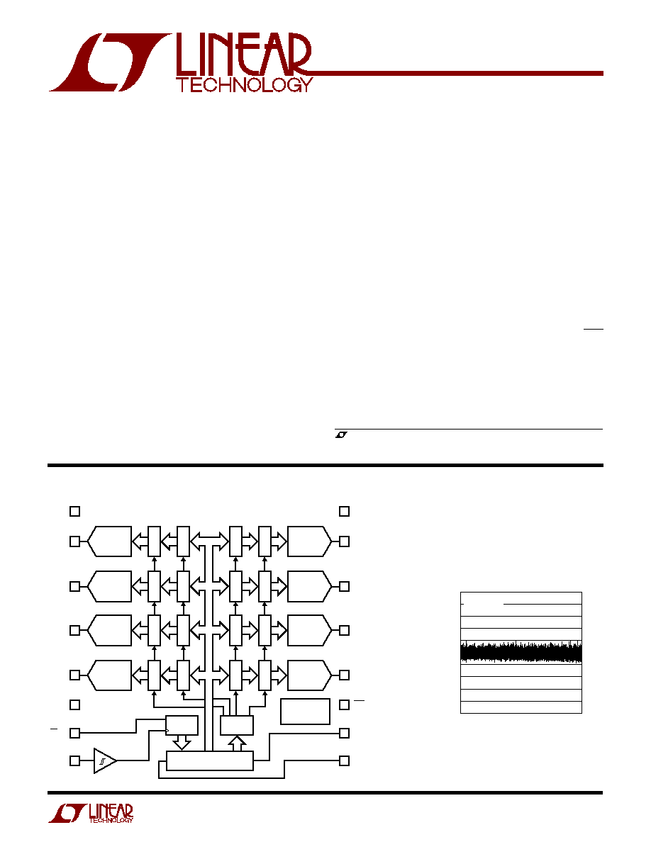
16
DAC A
3
14
4
13
5
7
6
8
10
11
9
12
DECODE
POWER-ON
RESET
CONTROL
LOGIC
32-BIT SHIFT REGISTER
REGISTER
REGISTER
DAC H
REGISTER
REGISTER
DAC B
REGISTER
REGISTER
DAC G
REGISTER
REGISTER
DAC C
REGISTER
REGISTER
DAC F
REGISTER
REGISTER
DAC D
REGISTER
REGISTER
DAC E
REGISTER
REGISTER
CODE
0
16384
32768
49152
65535
DNL (LSB)
2600 G21
1.0
0.8
0.6
0.4
0.2
0
≠0.2
≠0.4
≠0.6
≠0.8
≠1.0
V
CC
= 5V
V
REF
= 4.096V
MICROWIRE is a trademark of National Semiconductor Corporation.
APPLICATIO S
U
FEATURES
DESCRIPTIO
U
BLOCK DIAGRA
W
2
LTC2600/LTC2610/LTC2620
2600fa
A
U
G
W
A
W
U
W
A
R
BSOLUTE
XI
TI
S
ORDER PART
NUMBER
W
U
U
PACKAGE/ORDER I FOR ATIO
T
JMAX
= 125
∞
C,
JA
= 150
∞
C/W
(Note 1)
Any Pin to GND ........................................... ≠ 0.3V to 6V
Any Pin to V
CC
.............................................≠ 6V to 0.3V
Maximum Junction Temperature ......................... 125
∞
C
Operating Temperature Range
LTC2600C/LTC2610C/LTC2620C .......... 0
∞
C to 70
∞
C
LTC2600I/LTC2610I/LTC2620I .......... ≠ 40
∞
C to 85
∞
C
Storage Temperature Range ................ ≠ 65
∞
C to 150
∞
C
Lead Temperature (Soldering, 10 sec)................ 300
∞
C
GN PART MARKING
ELECTRICAL C
C
HARA TERISTICS
The
q
denotes specifications which apply over the full operating
temperature range, otherwise specifications are at T
A
= 25
∞
C. V
CC
= 2.5V to 5.5V, V
REF
V
CC
, V
OUT
unloaded, unless otherwise noted.
1
2
3
4
5
6
7
8
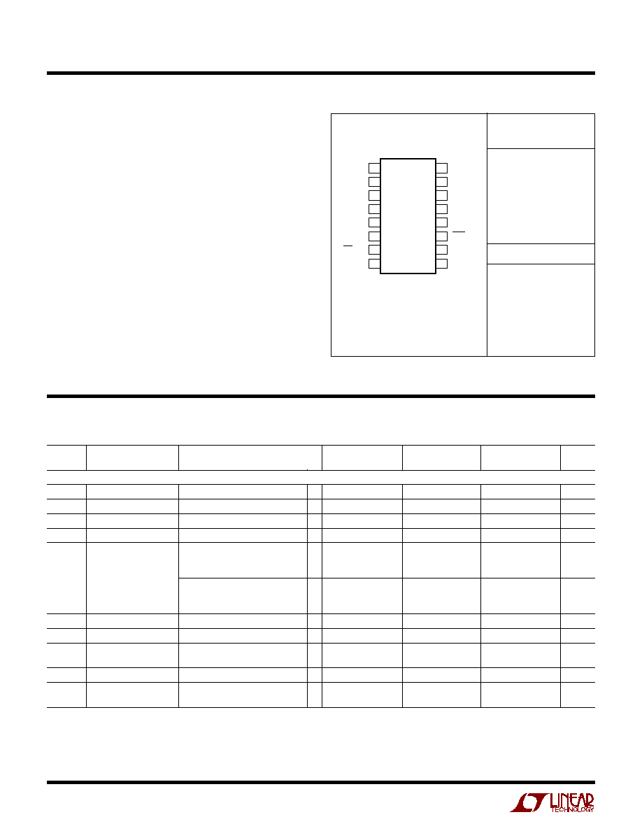
TOP VIEW
GN PACKAGE
16-LEAD PLASTIC SSOP
16
15
14
13
12
11
10
9
GND
V
OUT A
V
OUT B
V
OUT C
V
OUT D
REF
CS/LD
SCK
V
CC
V
OUT H
V
OUT G
V
OUT F
V
OUT E
CLR
SDO
SDI
LTC2600CGN
LTC2600IGN
LTC2610CGN
LTC2610IGN
LTC2620CGN
LTC2620IGN
2600
2600I
2610
2610I
2620
2620I
Consult LTC Marketing for parts specified with wider operating temperature ranges.
LTC2620
LTC2610
LTC2600
SYMBOL
PARAMETER
CONDITIONS
MIN
TYP
MAX
MIN
TYP
MAX
MIN
TYP
MAX
UNITS
DC Performance
Resolution
q
12
14
16
Bits
Monotonicity
V
CC
= 5V, V
REF
= 4.096V (Note 2)
q
12
14
16
Bits
DNL
Differential Nonlinearity
V
CC
= 5V, V
REF
= 4.096V (Note 2)
q
±
0.5
±
1
±
1
LSB
INL
Integral Nonlinearity
V
CC
= 5V, V
REF
= 4.096V (Note 2)
q
±
0.75
±
4
±
3
±
16
±
12
±
64
LSB
Load Regulation
V
REF
= V
CC
= 5V, Midscale
I
OUT
= 0mA to 15mA Sourcing
q
0.025 0.125
0.1
0.5
0.3
2
LSB/mA
I
OUT
= 0mA to 15mA Sinking
q
0.025 0.125
0.1
0.5
0.3
2
LSB/mA
V
REF
= V
CC
= 2.5V, Midscale
I
OUT
= 0mA to 7.5mA Sourcing
q
0.05
0.25
0.2
1
0.8
4
LSB/mA
I
OUT
= 0mA to 7.5mA Sinking
q
0.05
0.25
0.2
1
0.8
4
LSB/mA
ZSE
Zero-Scale Error
V
CC
= 5V, V
REF
= 4.096V Code = 0
q
1
9
1
9
1
9
mV
V
OS
Offset Error
V
CC
= 5V, V
REF
= 4.096V (Note 7)
q
±
1
±
9
±
1
±
9
±
1
±
9
mV
V
OS
Temperature
±
3
±
3
±
3
µ
V/
∞
C
Coefficient
GE
Gain Error
V
CC
= 5V, V
REF
= 4.096V
q
±
0.2
±
0.7
±
0.2
±
0.7
±
0.2
±
0.7
%FSR
Gain Temperature
±
6.5
±
6.5
±
6.5
ppm/
∞
C
Coefficient
3
LTC2600/LTC2610/LTC2620
2600fa
ELECTRICAL C
C
HARA TERISTICS
The
q
denotes specifications which apply over the full operating
temperature range, otherwise specifications are at T
A
= 25
∞
C. V
CC
= 2.5V to 5.5V, V
REF
V
CC
, V
OUT
unloaded, unless otherwise noted.
LTC2600/LTC2610/LTC2620
SYMBOL
PARAMETER
CONDITIONS
MIN
TYP
MAX
UNITS
PSR
Power Supply Rejection
V
CC
=
±
10%
≠80
dB
R
OUT
DC Output Impedance
V
REF
= V
CC
= 5V, Midscale; ≠15mA
I
OUT
15mA
q
0.025
0.15
V
REF
= V
CC
= 2.5V, Midscale; ≠7.5mA
I
OUT
7.5mA
q
0.030
0.15
DC Crosstalk (Note 4)
Due to Full Scale Output Change (Note 5)
±
10
µ
V
Due to Load Current Change
±
3.5
µ
V/mA
Due to Powering Down (per Channel)
±
7.3
µ
V
I
SC
Short-Circuit Output Current
V
CC
= 5.5V, V
REF
= 5.6V
Code: Zero Scale; Forcing Output to V
CC
q
15
34
60
mA
Code: Full Scale; Forcing Output to GND
q
15
34
60
mA
V
CC
= 2.5V, V
REF
= 2.6V
Code: Zero Scale; Forcing Output to V
CC
q
7.5
18
50
mA
Code: Full Scale; Forcing Output to GND
q
7.5
24
50
mA
Reference Input
Input Voltage Range
q
0
V
CC
V
Resistance
Normal Mode
q
11
16
20
k
Capacitance
90
pF
I
REF
Reference Current, Power Down Mode
All DACs Powered Down
q
0.001
1
µ
A
Power Supply
V
CC
Positive Supply Voltage
For Specified Performance
q
2.5
5.5
V
I
CC
Supply Current
V
CC
= 5V (Note 3)
q
2.6
4
mA
V
CC
= 3V (Note 3)
q
2.0
3.2
mA
All DACs Powered Down (Note 3) V
CC
= 5V
q
0.35
1
µ
A
All DACs Powered Down (Note 3) V
CC
= 3V
q
0.10
1
µ
A
Digital I/O
V
IH
Digital Input High Voltage
V
CC
= 2.5V to 5.5V
q
2.4
V
V
CC
= 2.5V to 3.6V
q
2.0
V
V
IL
Digital Input Low Voltage
V
CC
= 4.5V to 5.5V
q
0.8
V
V
CC
= 2.5V to 5.5V
q
0.6
V
V
OH
Digital Output High Voltage
Load Current = ≠100
µ
A
q
V
CC
≠ 0.4
V
V
OL
Digital Output Low Voltage
Load Current = +100
µ
A
q
0.4
V
I
LK
Digital Input Leakage
V
IN
= GND to V
CC
q
±
1
µ
A
C
IN
Digital Input Capacitance
(Note 6)
q
8
pF
4
LTC2600/LTC2610/LTC2620
2600fa
LTC2600/LTC2610/LTC2620
SYMBOL
PARAMETER
CONDITIONS
MIN
TYP
MAX
UNITS
V
CC
= 2.5V to 5.5V
t
1
SDI Valid to SCK Setup
q
4
ns
t
2
SDI Valid to SCK Hold
q
4
ns
t
3
SCK High Time
q
9
ns
t
4
SCK Low Time
q
9
ns
t
5
CS/LD Pulse Width
q
10
ns
t
6
LSB SCK High to CS/LD High
q
7
ns
t
7
CS/LD Low to SCK High
q
7
ns
t
8
SDO Propagation Delay from SCK Falling Edge
C
LOAD
= 10pF
V
CC
= 4.5V to 5.5V
q
20
ns
V
CC
= 2.5V to 5.5V
q
45
ns
t
9
CLR Pulse Width
q
20
ns
t
10
CS/LD High to SCK Positive Edge
q
7
ns
SCK Frequency
50% Duty Cycle
q
50
MHz
TI I G CHARACTERISTICS
U
W
The
q
denotes specifications which apply over the full operating temperature
range, otherwise specifications are at T
A
= 25
∞
C. (See Figure 1) (Note 6)
Note 1: Absolute maximum ratings are those values beyond which the life
of a device may be impaired.
Note 2: Linearity and monotonicity are defined from code k
L
to code
2
N
≠ 1, where N is the resolution and k
L
is given by k
L
= 0.016(2
N
/V
REF
),
rounded to the nearest whole code. For V
REF
= 4.096V and N = 16, k
L
=
256 and linearity is defined from code 256 to code 65,535.
Note 3: Digital inputs at 0V or V
CC
.
Note 4: DC crosstalk is measured with V
CC
= 5V and V
REF
= 4.096V, with
the measured DAC at midscale, unless otherwise noted.
Note 5: R
L
= 2k
to GND or V
CC
.
Note 6: Guaranteed by design and not production tested.
Note 7: Inferred from measurement at code 256 (LTC2600), code 64
(LTC2610) or code 16 (LTC2620), and at fullscale.
Note 8: V
CC
= 5V, V
REF
= 4.096V. DAC is stepped 1/4 scale to 3/4 scale
and 3/4 scale to 1/4 scale. Load is 2k in parallel with 200pF to GND.
Note 9: V
CC
= 5V, V
REF
= 4.096V. DAC is stepped
±
1LSB between half
scale and half scale ≠ 1. Load is 2k in parallel with 200pF to GND.
ELECTRICAL C
C
HARA TERISTICS
The
q
denotes specifications which apply over the full operating
temperature range, otherwise specifications are at T
A
= 25
∞
C. V
CC
= 2.5V to 5.5V, V
REF
V
CC
, V
OUT
unloaded, unless otherwise noted.
LTC2620
LTC2610
LTC2600
SYMBOL
PARAMETER
CONDITIONS
MIN
TYP
MAX
MIN
TYP
MAX
MIN
TYP
MAX
UNITS
AC Performance
t
S
Settling Time (Note 8)
±
0.024% (
±
1LSB at 12 Bits)
7
7
7
µ
s
±
0.006% (
±
1LSB at 14 Bits)
9
9
µ
s
±
0.0015% (
±
1LSB at 16 Bits)
10
µ
s
Settling Time for 1LSB Step
±
0.024% (
±
1LSB at 12 Bits)
2.7
2.7
2.7
µ
s
(Note 9)
±
0.006% (
±
1LSB at 14 Bits)
4.8
4.8
µ
s
±
0.0015% (
±
1LSB at 16 Bits)
5.2
µ
s
Voltage Output Slew Rate
0.80
0.80
0.80
V/
µ
s
Capacitive Load Driving
1000
1000
1000
pF
Glitch Impulse
At Midscale Transition
12
12
12
nV ∑ s
Multiplying Bandwidth
180
180
180
kHz
e
n
Output Voltage Noise Density
At f = 1kHz
120
120
120
nV/
Hz
At f = 10kHz
100
100
100
nV/
Hz
Output Voltage Noise
0.1Hz to 10Hz
15
15
15
µ
V
P-P
5
LTC2600/LTC2610/LTC2620
2600fa
TYPICAL PERFOR A CE CHARACTERISTICS
U
W
Settling to
±
1LSB
Settling of Full-Scale Step
2
µ
s/DIV
2600 G26
V
OUT
100
µ
V/DIV
CS/LD
2V/DIV
V
CC
= 5V, V
REF
= 4.096V
1/4-SCALE TO 3/4-SCALE STEP
R
L
= 2k, C
L
= 200pF
AVERAGE OF 2048 EVENTS
9.7
µ
s
5
µ
s/DIV
2600 G27
V
OUT
100
µ
V/DIV
CS/LD
2V/DIV
SETTLING TO
±
1LSB
V
CC
= 5V, V
REF
= 4.096V
CODE 512 TO 65535 STEP
R
L
= 2k, C
L
= 200pF
AVERAGE OF 2048 EVENTS
12.3
µ
s
LTC2600
CODE
0
16384
32768
49152
65535
INL (LSB)
2600 G20
32
24
16
8
0
≠8
≠16
≠24
≠32
V
CC
= 5V
V
REF
= 4.096V
CODE
0
16384
32768
49152
65535
DNL (LSB)
2600 G21
1.0
0.8
0.6
0.4
0.2
0
≠0.2
≠0.4
≠0.6
≠0.8
≠1.0
V
CC
= 5V
V
REF
= 4.096V
TEMPERATURE (
∞
C)
≠50
≠30
≠10
10
30
50
70
90
INL (LSB)
2600 G22
32
24
16
8
0
≠8
≠16
≠24
≠32
V
CC
= 5V
V
REF
= 4.096V
INL (POS)
INL (NEG)
TEMPERATURE (
∞
C)
≠50
≠30
≠10
10
30
50
70
90
DNL (LSB)
2600 G23
1.0
0.8
0.6
0.4
0.2
0
≠0.2
≠0.4
≠0.6
≠0.8
≠1.0
V
CC
= 5V
V
REF
= 4.096V
DNL (POS)
DNL (NEG)
V
REF
(V)
0
1
2
3
4
5
INL (LSB)
2600 G24
32
24
16
8
0
≠8
≠16
≠24
≠32
V
CC
= 5.5V
INL (POS)
INL (NEG)
V
REF
(V)
0
1
2
3
4
5
DNL (LSB)
2600 G25
1.5
1.0
0.5
0
≠0.5
≠1.0
≠1.5
V
CC
= 5.5V
DNL (POS)
DNL (NEG)
Integral Nonlinearity (INL)
Differential Nonlinearity (DNL)
INL vs Temperature
DNL vs Temperature
INL vs V
REF
DNL vs V
REF

6
LTC2600/LTC2610/LTC2620
2600fa
TYPICAL PERFOR A CE CHARACTERISTICS
U
W
Integral Nonlinearity (INL)
Differential Nonlinearity (DNL)
LTC2620
CODE
0
1024
2048
3072
4095
INL (LSB)
2600 G31
2.0
1.5
1.0
0.5
0
≠0.5
≠1.0
≠1.5
≠2.0
V
CC
= 5V
V
REF
= 4.096V
CODE
0
1024
2048
3072
4095
DNL (LSB)
2600 G32
V
CC
= 5V
V
REF
= 4.096V
1.0
0.8
0.6
0.4
0.2
0
≠0.2
≠0.4
≠0.6
≠0.8
≠1.0
LTC2610
CODE
0
4096
8192
12288
16383
INL (LSB)
2600 G28
8
6
4
2
0
≠2
≠4
≠6
≠8
V
CC
= 5V
V
REF
= 4.096V
CODE
0
4096
8192
12288
16383
DNL (LSB)
2600 G29
1.0
0.8
0.6
0.4
0.2
0
≠0.2
≠0.4
≠0.6
≠0.8
≠1.0
V
CC
= 5V
V
REF
= 4.096V
Integral Nonlinearity (INL)
Differential Nonlinearity (DNL)
Settling to
±
1LSB
Settling to
±
1LSB
2
µ
s/DIV
2600 G30
V
OUT
100
µ
V/DIV
CS/LD
2V/DIV
V
CC
= 5V, V
REF
= 4.096V
1/4-SCALE TO 3/4-SCALE STEP
R
L
= 2k, C
L
= 200pF
AVERAGE OF 2048 EVENTS
8.9
µ
s
2
µ
s/DIV
2600 G33
V
OUT
1mV/DIV
CS/LD
2V/DIV
V
CC
= 5V, V
REF
= 4.096V
1/4-SCALE TO 3/4-SCALE STEP
R
L
= 2k, C
L
= 200pF
AVERAGE OF 2048 EVENTS
6.8
µ
s
LTC2600/LTC2610/LTC2620
Current Limiting
Load Regulation
Offset Error vs Temperature
TEMPERATURE (
∞
C)
≠50
≠30
≠10
10
30
50
70
90
OFFSET ERROR (mV)
2600 G03
3
2
1
0
≠1
≠2
≠3
I
OUT
(mA)
≠40 ≠30 ≠20 ≠10
0
10
20
30
40
V
OUT
(V)
2600 G01
0.10
0.08
0.06
0.04
0.02
0
≠0.02
≠0.04
≠0.06
≠0.08
≠0.10
V
REF
= V
CC
= 5V
V
REF
= V
CC
= 3V
V
REF
= V
CC
= 5V
V
REF
= V
CC
= 3V
CODE = MIDSCALE
I
OUT
(mA)
≠35
≠25
≠15
≠5
5
15
25
35
V
OUT
(mV)
2600 G02
1.0
0.8
0.6
0.4
0.2
0
≠0.2
≠0.4
≠0.6
≠0.8
≠1.0
V
REF
= V
CC
= 5V
CODE = MIDSCALE
V
REF
= V
CC
= 3V
7
LTC2600/LTC2610/LTC2620
2600fa
TYPICAL PERFOR A CE CHARACTERISTICS
U
W
Gain Error vs Temperature
Offset Error vs V
CC
TEMPERATURE (
∞
C)
≠50
≠30
≠10
10
30
50
70
90
GAIN ERROR (%FSR)
2600 G05
0.4
0.3
0.2
0.1
0
≠0.1
≠0.2
≠0.3
≠0.4
TEMPERATURE (
∞
C)
≠50
≠30
≠10
10
30
50
70
90
ZERO-SCALE ERROR (mV)
2600 G04
3
2.5
2.0
1.5
1.0
0.5
0
Zero-Scale Error vs Temperature
V
CC
(V)
2.5
3
3.5
4
4.5
5
5.5
OFFSET ERROR (mV)
2600 G06
3
2
1
0
≠1
≠2
≠3
V
CC
(V)
2.5
3
3.5
4
4.5
5
5.5
GAIN ERROR (%FSR)
2600 G07
0.4
0.3
0.2
0.1
0
≠0.1
≠0.2
≠0.3
≠0.4
V
CC
(V)
2.5
3
3.5
4
4.5
5
5.5
I
CC
(nA)
2600 G08
450
400
350
300
250
200
150
100
50
0
2.5
µ
s/DIV
V
OUT
0.5V/DIV
2600 G09
V
REF
= V
CC
= 5V
1/4-SCALE TO 3/4-SCALE
I
CC
Shutdown vs V
CC
Large-Signal Response
Gain Error vs V
CC
LTC2600/LTC2610/LTC2620
Midscale Glitch Impulse
Power-On Reset Glitch
Headroom at Rails
vs Output Current
V
OUT
10mV/DIV
CS/LD
5V/DIV
2.5
µ
s/DIV
2600 G10
12nV-s TYP
V
OUT
10mV/DIV
250
µ
s/DIV
2600 G11
V
CC
1V/DIV
4mV PEAK
4mV PEAK
I
OUT
(mA)
0
1
2
3
4
5
6
7
8
9
10
V
OUT
(V)
2600 G12
5.0
4.5
4.0
3.5
3.0
2.5
2.0
1.5
1.0
0.5
0
5V SOURCING
3V SOURCING
3V SINKING
5V SINKING
8
LTC2600/LTC2610/LTC2620
2600fa
TYPICAL PERFOR A CE CHARACTERISTICS
U
W
1V/DIV
10mA/DIV
0mA
2600 G18
V
CC
= 5.5V
V
REF
= 5.6V
CODE = 0
V
OUT
SWEPT 0V TO V
CC
1V/DIV
10mA/DIV
0mA
2600 G19
V
CC
= 5.5V
V
REF
= 5.6V
CODE = FULL SCALE
V
OUT
SWEPT V
CC
TO 0V
Short-Circuit Output Current vs
V
OUT
(Sinking)
Short-Circuit Output Current vs
V
OUT
(Sourcing)
Supply Current vs Logic Voltage
Exiting Power-Down to Midscale
Hardware CLR
V
OUT
1V/DIV
1
µ
s/DIV
2600 G15
CLR
5V/DIV
LOGIC VOLTAGE (V)
0
0.5
1
1.5
2
2.5
3
3.5
4
4.5
5
I
CC
(mA)
2600 G13
2.4
2.3
2.2
2.1
2.0
1.9
1.8
1.7
1.6
1.5
V
CC
= 5V
SWEEP SCK, SDI
AND CS/LD
0V TO V
CC
2.5
µ
s/DIV
V
OUT
0.5V/DIV
CS/LD
5V/DIV
2600 G14
V
CC
= 5V
V
REF
= 2V
DACs A TO G IN
POWER-DOWN MODE
V
OUT
10
µ
V/DIV
SECONDS
0
1
2
3
4
5
6
7
8
9
10
2600 G17
FREQUENCY (Hz)
1k
dB
0
≠3
≠6
≠9
≠12
≠15
≠18
≠21
≠24
≠27
≠30
≠33
≠36
1M
2600 G16
10k
100k
V
CC
= 5V
V
REF
(DC) = 2V
V
REF
(AC) = 0.2V
P-P
CODE = FULL SCALE
Multiplying Bandwidth
Output Voltage Noise,
0.1Hz to 10Hz
LTC2600/LTC2610/LTC2620

9
LTC2600/LTC2610/LTC2620
2600fa
PI
N
FU
N
CTIO
N
S
U
U
U
GND (Pin 1): Analog Ground.
V
OUT A
to V
OUT H
(Pins 2-5 and 12-15): DAC Analog
Voltage Outputs. The output range is 0 ≠ V
REF
.
REF (Pin 6): Reference Voltage Input. 0V
V
REF
V
CC
.
CS/LD (Pin 7): Serial Interface Chip Select/Load Input.
When CS/LD is low, SCK is enabled for shifting data on SDI
into the register. When CS/LD is taken high, SCK is dis-
abled and the specified command (see Table 1) is ex-
ecuted.
SCK (Pin 8): Serial Interface Clock Input. CMOS and TTL
compatible.
SDI (Pin 9): Serial Interface Data Input. Data is applied to
SDI for transfer to the device at the rising edge of SCK. The
LTC2600, LTC2610 and LTC2620 accept input word lengths
of either 24 or 32 bits.
SDO (Pin 10): Serial Interface Data Output. The serial
output of the shift register appears at the SDO pin. The data
transferred to the device via the SDI pin is delayed 32 SCK
rising edges before being output at the next falling edge.
This pin is used for daisy-chain operation.
CLR (Pin 11): Asynchronous Clear Input. A logic low at
this level-triggered input clears all registers and causes
the DAC voltage outputs to drop to 0V. CMOS and TTL
compatible.
V
CC
(Pin 16): Supply Voltage Input. 2.5V
V
CC
5.5V.
10
LTC2600/LTC2610/LTC2620
2600fa
BLOCK DIAGRA
W
2
15
1
GND
V
OUT A
V
OUT B
V
OUT C
V
OUT D
REF
CS/LD
SCK
V
CC
V
OUT H
V
OUT G
V
OUT F
V
OUT E
CLR
SDO
SDI
2600 BD02
16
DAC A
3
14
4
13
5
7
6
8
10
11
9
12
DECODE
CONTROL
LOGIC
32-BIT SHIFT REGISTER
DAC
REGISTER
INPUT
REGISTER
DAC H
DAC
REGISTER
INPUT
REGISTER
DAC B
DAC
REGISTER
INPUT
REGISTER
DAC G
DAC
REGISTER
INPUT
REGISTER
DAC C
DAC
REGISTER
INPUT
REGISTER
DAC F
DAC
REGISTER
INPUT
REGISTER
DAC D
DAC
REGISTER
INPUT
REGISTER
DAC E
DAC
REGISTER
INPUT
REGISTER
POWER-ON
RESET
TI I G DIAGRA
U
W
W
Figure 1
SDI
SDO
CS/LD
SCK
2600 F01
t
2
t
8
t
10
t
5
t
7
t
6
t
1
t
3
t
4
1
2
3
23
24
11
LTC2600/LTC2610/LTC2620
2600fa
Table 1.
COMMAND*
C3
C2
C1
C0
0
0
0
0
Write to Input Register n
0
0
0
1
Update (Power Up) DAC Register n
0
0
1
0
Write to Input Register n, Update (Power Up) All n
0
0
1
1
Write to and Update (Power Up) n
0
1
0
0
Power Down n
1
1
1
1
No Operation
ADDRESS (n)*
A3
A2
A1
A0
0
0
0
0
DAC A
0
0
0
1
DAC B
0
0
1
0
DAC C
0
0
1
1
DAC D
0
1
0
0
DAC E
0
1
0
1
DAC F
0
1
1
0
DAC G
0
1
1
1
DAC H
1
1
1
1
All DACs
Serial Interface
The CS/LD input is level triggered. When this input is taken
low, it acts as a chip-select signal, powering-on the SDI
and SCK buffers and enabling the input shift register. Data
(SDI input) is transferred at the next 24 rising SCK edges.
The 4-bit command, C3-C0, is loaded first; then the 4-bit
DAC address, A3-A0; and finally the 16-bit data word. The
data word comprises the 16-, 14- or 12-bit input code,
ordered MSB-to-LSB, followed by 0, 2 or 4 don't-care bits
(LTC2600, LTC2610 and LTC2620 respectively). Data can
only be transferred to the device when the CS/LD signal is
low.The rising edge of CS/LD ends the data transfer and
causes the device to carry out the action specified in the
24-bit input word. The complete sequence is shown in
Figure 2a.
The command (C3-C0) and address (A3-A0) assignments
are shown in Table 1. The first four commands in the table
consist of write and update operations. A write operation
loads a 16-bit data word from the 32-bit shift register into
the input register of the selected DAC, n. An update
operation copies the data word from the input register to
the DAC register. Once copied into the DAC register, the
data word becomes the active 16-, 14- or 12-bit input
code, and is converted to an analog voltage at the DAC
output. The update operation also powers up the selected
DAC if it had been in power-down mode. The data path and
registers are shown in the block diagram.
While the minimum input word is 24 bits, it may optionally
be extended to 32 bits. To use the 32-bit word width,
8 don't-care bits are transferred to the device first, fol-
lowed by the 24-bit word as just described. Figure 2b
OPERATIO
U
Power-On Reset
The LTC2600/LTC2610/LTC2620 clear the outputs to zero
scale when power is first applied, making system initializa-
tion consistent and repeatable.
For some applications, downstream circuits are active
during DAC power-up, and may be sensitive to nonzero
outputs from the DAC during this time. The LTC2600/
2610/2620 contain circuitry to reduce the power-on glitch:
the analog outputs typically rise less than 10mV above
zero scale during power on if the power supply is ramped
to 5V in 1ms or more. In general, the glitch amplitude
decreases as the power supply ramp time is increased.
See Power-On Reset Glitch in the Typical Performance
Characteristics section.
Power Supply Sequencing
The voltage at REF (Pin 6) should be kept within the range
≠ 0.3V
V
REF
V
CC
+ 0.3V (see Absolute Maximum
Ratings). Particular care should be taken to observe these
limits during power supply turn-on and turn-off sequences,
when the voltage at V
CC
(Pin 16) is in transition.
Transfer Function
The digital-to-analog transfer function is
V
k
V
OUT IDEAL
N
REF
(
)
=
2
where k is the decimal equivalent of the binary DAC input
code, N is the resolution and V
REF
is the voltage at REF
(Pin 6).
*Command and address codes not shown are reserved and should not be used.
12
LTC2600/LTC2610/LTC2620
2600fa
OPERATIO
U
C3
COMMAND
ADDRESS
DATA (16 BITS)
C2
C1
C0 A3 A2 A1
A0
D13
D14
D15
D12 D11 D10 D9
D8
D7 D6
D5
D4
D3
D2
D1 D0
2600 TBL01
MSB
LSB
INPUT WORD (LTC2600)
shows the 32-bit sequence. The 32-bit word is required for
daisy-chain operation, and is also available to accommo-
date microprocessors which have a minimum word width
of 16 bits (2 bytes).
Daisy-Chain Operation
The serial output of the shift register appears at the SDO
pin. Data transferred to the device from the SDI input is
delayed 32 SCK rising edges before being output at the
next SCK falling edge.
The SDO output can be used to facilitate control of multiple
serial devices from a single 3-wire serial port (i.e., SCK,
SDI and CS/LD). Such a "daisy chain" series is configured
by connecting SDO of each upstream device to SDI of the
next device in the chain. The shift registers of the devices
are thus connected in series, effectively forming a single
input shift register which extends through the entire chain.
Because of this, the devices can be addressed and con-
trolled individually by simply concatenating their input
words; the first instruction addresses the last device in the
chain and so forth. The SCK and CS/LD signals are
common to all devices in the series.
In use, CS/LD is first taken low. Then the concatenated
input data is transferred to the chain, using SDI of the first
device as the data input. When the data transfer is com-
plete, CS/LD is taken high, completing the instruction
sequence for all devices simultaneously. A single device
can be controlled by using the no-operation command
(1111) for the other devices in the chain.
Power-Down Mode
For power-constrained applications, power-down mode
can be used to reduce the supply current whenever less
than eight outputs are needed. When in power-down, the
buffer amplifiers and reference inputs are disabled, and
draw essentially zero current. The DAC outputs are put into
a high-impedance state, and the output pins are passively
pulled to ground through individual 90k resistors. When
all eight DACs are powered down, the master bias genera-
tion circuit is also disabled. Input- and DAC-register
contents are not disturbed during power-down.
Any channel or combination of channels can be put into
power-down mode by using command 0100
b
in combina-
tion with the appropriate DAC address, (n). The 16-bit data
word is ignored. The supply and reference currents are
reduced by approximately 1/8 for each DAC powered
down; the effective resistance at REF (pin 6) rises accord-
ingly, becoming a high-impedance input (typically > 1G
)
when all eight DACs are powered down.
Normal operation can be resumed by executing any com-
mand which includes a DAC update, as shown in Table 1.
INPUT WORD (LTC2610)
INPUT WORD (LTC2620)
C3
COMMAND
ADDRESS
DATA (14 BITS + 2 DON'T-CARE BITS)
C2
C1
C0 A3 A2 A1
A0
D13 D12 D11 D10 D9
D8
D7 D6
D5
D4
D3
D2
D1 D0
X
X
2600 TBL02
MSB
LSB
C3
COMMAND
ADDRESS
DATA (12 BITS + 4 DON'T-CARE BITS)
C2
C1
C0 A3 A2 A1
A0
D11 D10 D9
D8
D7 D6
D5
D4
D3
D2
D1 D0
X
X
X
X
2600 TBL03
MSB
LSB

13
LTC2600/LTC2610/LTC2620
2600fa
The selected DAC is powered up as its voltage output is
updated.
There is an initial delay as the DAC powers up before it
begins its usual settling behavior. If less than eight DACs
are in a powered-down state prior to the update command,
the power-up delay is 5
µ
s. If, on the other hand, all eight
DACs are powered down, then the master bias generation
circuit is also disabled and must be restarted. In this case,
the power-up delay is greater: 12
µ
s for V
CC
= 5V, 30
µ
s for
V
CC
= 3V.
Voltage Outputs
Each of the 8 rail-to-rail amplifiers contained in these parts
has guaranteed load regulation when sourcing or sinking
up to 15mA at 5V (7.5mA at 3V).
Load regulation is a measure of the amplifier's ability to
maintain the rated voltage accuracy over a wide range of
load conditions. The measured change in output voltage
per milliampere of forced load current change is ex-
pressed in LSB/mA.
DC output impedance is equivalent to load regulation, and
may be derived from it by simply calculating a change in
units from LSB/mA to Ohms. The amplifiers' DC output
impedance is 0.025
when driving a load well away from
the rails.
When drawing a load current from either rail, the output
voltage headroom with respect to that rail is limited by the
25
typical channel resistance of the output devices; e.g.,
when sinking 1mA, the minimum output voltage = 25
∑
1mA = 25mV. See the graph Headroom at Rails vs Output
Current in the Typical Performance Characteristics sec-
tion.
The amplifiers are stable driving capacitive loads of up to
1000pF.
Board Layout
The excellent load regulation and DC crosstalk perfor-
mance of these devices is achieved in part by keeping
"signal" and "power" grounds separated internally and by
reducing shared internal resistance to just 0.005
.
The GND pin functions both as the node to which the
reference and output voltages are referred and as a return
path for power currents in the device. Because of this,
careful thought should be given to the grounding scheme
and board layout in order to ensure rated performance.
The PC board should have separate areas for the analog
and digital sections of the circuit. This keeps digital signals
away from sensitive analog signals and facilitates the use
of separate digital and analog ground planes which have
minimal capacitive and resistive interaction with each
other.
Digital and analog ground planes should be joined at only
one point, establishing a system star ground as close to
the device's ground pin as possible. Ideally, the analog
ground plane should be located on the component side of
the board, and should be allowed to run under the part to
shield it from noise. Analog ground should be a continu-
ous and uninterrupted plane, except for necessary lead
pads and vias, with signal traces on another layer.
The GND pin of the part should be connected to analog
ground. Resistance from the GND pin to system star
ground should be as low as possible. Resistance here will
add directly to the effective DC output impedance of the
device (typically 0.025
), and will degrade DC crosstalk.
Note that the LTC2600/LTC2610/LTC2620 are no more
susceptible to these effects than other parts of their type;
on the contrary, they allow layout-based performance
improvements to shine rather than limiting attainable
performance with excessive internal resistance.
Rail-to-Rail Output Considerations
In any rail-to-rail voltage output device, the output is
limited to voltages within the supply range.
Since the analog outputs of the device cannot go below
ground, they may limit for the lowest codes as shown in
Figure 3b. Similarly, limiting can occur near full scale
when the REF pin is tied to V
CC
. If V
REF
= V
CC
and the DAC
full-scale error (FSE) is positive, the output for the highest
codes limits at V
CC
as shown in Figure 3c. No full-scale
limiting can occur if V
REF
is less than V
CC
≠ FSE.
Offset and linearity are defined and tested over the region
of the DAC transfer function where no output limiting can
occur.
OPERATIO
U

14
LTC2600/LTC2610/LTC2620
2600fa
1
2
3
4
5
6
7
8
9
10
11
12
13
14
15
16
17
18
19
20
21
22
23
24
25
26
27
28
29
30
31
32
C2
C1
C0
A3
A2
A1
A0
D15
D14
D13
D12
D11
D10
D9
D8
D7
D6
D5
D4
D3
D2
D1
D0
C3
X
X
X
X
X
X
X
X
CS/LD
SCK
SDI
COMMAND WORD
ADDRESS WORD
DATA WORD
DON'T CARE
C2
C1
C0
A3
A2
A1
A0
D15
D14
D13
D12
D11
D10
D9
D8
D7
D6
D5
D4
D3
D2
D1
D0
C3
X
X
X
X
X
X
X
X
SDO
CURRENT
32-BIT
INPUT WORD
YYYY F02b
PREVIOUS 32-BIT INPUT WORD
t
2
t
3
t
4
t
1
t
8
D15
17
SCK
SDI
SDO
PREVIOUS D14
PREVIOUS D15
18
D14
Figure 2b. LTC2600 32-Bit Load Sequence (Required for Daisy-Chain Operation).
LTC2610 SDI/SDO Data Word: 14-Bit Input Code + 2 Don't-Care Bits;
LTC2620 SDI/SDO Data Word: 12-Bit Input Code + 4 Don't-Care Bits
OPERATIO
U
1
2
3
4
5
6
7
8
9
10
11
12
13
14
15
16
17
18
19
20
21
22
23
24
C2
C1
C0
A3
A2
A1
A0
D15
D14
D13
D12
D11
D10
D9
D8
D7
D6
D5
D4
D3
D2
D1
D0
C3
CS/LD
SCK
SDI
COMMAND WORD
ADDRESS WORD
DATA WORD
24-BIT INPUT WORD
YYYY F02a
Figure 2a. LTC2600 24-Bit Load Sequence (Minimum Input Word).
LTC2610 SDI Data Word: 14-Bit Input Code + 2 Don't-Care Bits;
LTC2620 SDI Data Word: 12-Bit Input Code + 4 Don't-Care Bits
15
LTC2600/LTC2610/LTC2620
2600fa
U
PACKAGE DESCRIPTIO
GN Package
16-Lead Plastic SSOP (Narrow .150 Inch)
(Reference LTC DWG # 05-08-1641)
GN16 (SSOP) 0502
1
2
3
4
5
6
7
8
.229 ≠ .244
(5.817 ≠ 6.198)
.150 ≠ .157**
(3.810 ≠ 3.988)
16 15 14 13
.189 ≠ .196*
(4.801 ≠ 4.978)
12 11 10 9
.016 ≠ .050
(0.406 ≠ 1.270)
.015
±
.004
(0.38
±
0.10)
◊
45
∞
0
∞
≠ 8
∞
TYP
.007 ≠ .0098
(0.178 ≠ 0.249)
.053 ≠ .068
(1.351 ≠ 1.727)
.008 ≠ .012
(0.203 ≠ 0.305)
.004 ≠ .0098
(0.102 ≠ 0.249)
.0250
(0.635)
BSC
.009
(0.229)
REF
.254 MIN
RECOMMENDED SOLDER PAD LAYOUT
.150 ≠ .165
.0250 TYP
.0165
±
.0015
.045
±
.005
*DIMENSION DOES NOT INCLUDE MOLD FLASH. MOLD FLASH
SHALL NOT EXCEED 0.006" (0.152mm) PER SIDE
**DIMENSION DOES NOT INCLUDE INTERLEAD FLASH. INTERLEAD
FLASH SHALL NOT EXCEED 0.010" (0.254mm) PER SIDE
INCHES
(MILLIMETERS)
NOTE:
1. CONTROLLING DIMENSION: INCHES
2. DIMENSIONS ARE IN
3. DRAWING NOT TO SCALE
2600 F03
INPUT CODE
(b)
OUTPUT
VOLTAGE
NEGATIVE
OFFSET
0V
32, 768
0
65, 535
INPUT CODE
OUTPUT
VOLTAGE
(a)
V
REF
= V
CC
V
REF
= V
CC
(c)
INPUT CODE
OUTPUT
VOLTAGE
POSITIVE
FSE
Figure 3. Effects of Rail-to-Rail Operation On a DAC Transfer Curve. (a) Overall Transfer Function (b) Effect
of Negative Offset for Codes Near Zero Scale (c) Effect of Positive Full-Scale Error for Codes Near Full Scale
OPERATIO
U
Information furnished by Linear Technology Corporation is believed to be accurate and reliable.
However, no responsibility is assumed for its use. Linear Technology Corporation makes no represen-
tation that the interconnection of its circuits as described herein will not infringe on existing patent rights.
16
LTC2600/LTC2610/LTC2620
2600fa
PART NUMBER
DESCRIPTION
COMMENTS
LTC1458/LTC1458L
Quad 12-Bit Rail-to-Rail Output DACs with Added Functionality
LTC1458: V
CC
= 4.5V to 5.5V, V
OUT
= 0V to 4.096V
LTC1458L: V
CC
= 2.7V to 5.5V, V
OUT
= 0V to 2.5V
LTC1654
Dual 14-Bit Rail-to-Rail V
OUT
DAC
Programmable Speed/Power, 3.5
µ
s/750
µ
A, 8
µ
s/450
µ
A
LTC1655/LTC1655L
Single 16-Bit V
OUT
DAC with Serial Interface in SO-8
V
CC
= 5V(3V), Low Power, Deglitched
LTC1657/LTC1657L
Parrallel 5V/3V 16-Bit V
OUT
DAC
Low Power, Deglitched, Rail-to-Rail V
OUT
LTC1660/LTC1665
Octal 10/8-Bit V
OUT
DAC in 16-Pin Narrow SSOP
V
CC
= 2.7V to 5.5V, Micropower, Rail-to-Rail Output
LTC1821
Parallel 16-Bit Voltage Output DAC
Precision 16-Bit Settling in 2
µ
s for 10V Step
©
LINEAR TECHNOLOGY CORPORATION 2003
LT/TP 1103 1K REV A ∑ PRINTED IN THE USA
Linear Technology Corporation
1630 McCarthy Blvd., Milpitas, CA 95035-7417
(408) 432-1900
q
FAX: (408) 434-0507
q
www.linear.com
RELATED PARTS
Schematic for LTC2600 Demonstration Circuit DC579. The Outputs Are Measured by an Onboard LTC2428
DISABLE
ADC
4.096V
5V
CS
SCK
MISO
MOSI
CS
SCK
V
CC
V
IN
V
IN
5V
V
CC
V
REF
V
REF
5V
R3
R6
7.5k
R5
7.5k
C10
100pF
R8
22
R4
TP4
DAC B
1
U1
24LC025
1
6
3
4
5
2
7
8
A0
SCL
A2
V
SS
SDA
A1
WP
V
CC
U5
LT1461ACS8-4
2
4
6
3
V
IN
GND
V
OUT
SHDN
TP5
DAC C
1
TP6
DAC D
1
R1
R1, R3, R4
are 4.99k, 1%
TP7
DAC E
1
LTC2424/LTC2428
U3
LTC2428CG
13
12
1
5
6
7
8
9
10
15
4
3
2
11
14
17
18
19
20
21
22
23
24
25
26
27
28
16
CH4
CH3
GND
ZS
SET
FS
SET
GND
MUXOUT
CH0
CH1
CH6
ADCIN
V
CC
V
CC
V
CC
V
REF
V
CC
CH2
CH5
CH7
GND
CLK
CSMUX
D
IN
GND
CSADC
SD0
SCK
FO
GND GND
GND
JP1
ON/OFF
C1
0.1
µ
F
C3
0.1
µ
F
R2
7.5k
C2
0.1
µ
F
C5
0.1
µ
F
C4
0.1
µ
F
TP8
DAC F
1
TP9
DAC G
1
TP3
DAC A
1
J1
HD2X7
1
3
5
7
9
11
13
2
4
6
8
10
12
14
+
+
+
+
+
+
+
+
+
+
+
+
+
+
JP2
V
REF
TP10
DAC H
1
TP16
U2
LTC2600CGN
13
12
5
6
1
7
8
9
10
15
16
4
3
2
11
14
V
OUT
F
V
OUT
E
GND
V
OUT
D
REF
LS/LD
SCK
SDI
SDO
V
OUT
H
V
CC
V
OUT
C
V
OUT
B
V
OUT
A
CLR
V
OUT
G
TP14
GND
1
TP15
GND
1
1
TP2
1
TP1
1
4-/8-CHANNEL
MUX
3
1
2
R7
7.5k
20-BIT
ADC
+
≠
3
1
2
TP13
GND
1
TP11
V
REF
1
C8
1
µ
F
16V
C9
0.1
µ
F
U4
LT1236ACS8-5
2
4
6
V
IN
GND
V
OUT
C6
0.1
µ
F
C7
4.7
µ
F
6.3V
REGULATOR
5V
REF
V
CC
JP3
V
CC
3
1
2
TP12
V
CC
1
U
TYPICAL APPLICATIO