 | ÐлекÑÑоннÑй компоненÑ: LTC3214 | СкаÑаÑÑ:  PDF PDF  ZIP ZIP |
3214.pm65

LTC3214
1
3214f
TYPICAL APPLICATIO
U
APPLICATIO S
U
FEATURES
DESCRIPTIO
U
LED Torch/Camera Light Supply for Cell Phones,
PDAs and Digital Cameras
General Lighting and/or Flash/Strobe Applications
Low Noise Constant Frequency Operation*
High Efficiency: Up to 94%
Multi-Mode Operation: 1x, 1.5x or 2x Boost Modes
Automatic Mode Switching
High Output Current: Up to 500mA
Tiny Application Circuit (3mm
× 3mm DFN Package,
All Components <1mm High)
Automatic Soft-Start
Output Disconnect
Open, Shorted LED Protection
No Inductors
Internal 110m
LED Current Sense Resistor
3mm
× 3mm 10-Lead DFN Package
500mA Camera
LED Charge Pump
The LTC
®
3214 is a low noise, high current charge pump
DC/DC converter capable of driving high current LEDs at
up to 500mA from a 2.9V to 4.5V input. Low external
parts count (two flying capacitors, one programming
resistor and two bypass capacitors at V
IN
and CPO) make
the LTC3214 ideally suited for small, battery-powered
applications.
Built-in soft-start circuitry prevents excessive inrush cur-
rent during start-up. High switching frequency enables the
use of small external capacitors.
Output current level is programmed by an external resis-
tor. LED current is regulated using an internal 110m
sense resistor. Automatic mode switching optimizes effi-
ciency by monitoring the voltage across the charge pump
and switching modes only when dropout is detected. The
part is available in a low profile 3mm x 3mm 10-lead DFN
package.
Efficiency vs V
IN
C1
2.2
µF
C2
2.2
µF
C
IN
2.2
µF
C
CPO
4.7
µF
I
LED
UP TO
500mA
LED
I
LED
V
IN
2.9V TO 4.5V
EN
DISABLE ENABLE
LTC3214
C1
+
C1
C2
+
C2
I
SET
3214 TA01a
LED: AOT2015
CPO
R
SET
0.11
, LTC and LT are registered trademarks of Linear Technology Corporation.
All other trademarks are the property of their respective owners.
*Protected by U.S. Patents including 6411531.
V
IN
(V)
2.9
EFFICIENCY (P
LED
/P
IN
) (%)
100
90
80
70
60
50
40
30
20
10
0
3.3
3.7
3.9
3214 TA01b
3.1
3.5
4.1
4.3
4.5
100mA
50mA
300mA
200mA
LED = AOT2015
V
F
= 2.9V TYP AT 100mA

LTC3214
2
3214f
V
IN
to GND ............................................... 0.3V to 5.5V
CPO to GND ............................................. 0.3V to 5.5V
EN ................................................... 0.3V to V
IN
+ 0.3V
I
CPO
, I
ILED
(Note 2) ............................................. 600mA
CPO Short-Circuit Duration ............................ Indefinite
Storage Temperature Range ................. 65
°C to 125°C
Operating Temperature Range (Note 3) .. 40
°C to 85°C
ABSOLUTE AXI U
RATI GS
W
W
W
U
PACKAGE/ORDER I FOR ATIO
U
U
W
(Note 1)
ELECTRICAL CHARACTERISTICS
The
denotes the specifications which apply over the full operating
temperature range, otherwise specifications are at T
A
= 25
°C. V
IN
= 3.6V, C
IN
= C1 = C2 = 2.2
µF, C
CPO
= 4.7
µF.
PARAMETER
CONDITIONS
MIN
TYP
MAX
UNITS
Input Power Supply
V
IN
Operating Voltage
2.9
4.5
V
I
VIN
Operating Current
I
CPO
= 0mA, 1x Mode
980
µA
I
CPO
= 0mA, 1.5x
4.8
mA
I
CPO
= 0mA, 2x Mode
6.7
mA
I
VIN
Shutdown Current
EN = LOW
2.5
7.5
µA
LED Current
LED Current Ratio (I
LED
/I
SET
)
I
LED
= 150mA to 500mA
2715
2950
3190
mA/mA
I
LED
Dropout Voltage (V
ILED
)
Mode Switch Threshold, I
LED
= 200mA
40
mV
Mode Switching Delay (LED Warmup Time)
2.5
ms
LED Current On Time
EN to LED Current On
100
µs
Charge Pump (CPO)
Charge Pump Output Clamp Voltage
5
V
1x Mode Output Impedance
0.70
1.5x Mode Output Impedance
3.2
2x Mode Output Impedance
4
CLK Frequency
V
IN
= 3V
0.6
0.9
1.2
MHz
EN
High Level Input Voltage (V
IH
)
1.4
V
Low Level Input Voltage (V
IL
)
0.4
V
Input Current (I
IH
)
V
EN
= 3.6V
14.4
20
µA
Input Current (I
IL
)
1
1
µA
T
JMAX
= 125
°C,
JA
= 43
°C/W
EXPOSED PAD (PIN 11) IS GND, MUST BE SOLDERED TO PCB GND
ORDER PART NUMBER
DD PART MARKING
Consult LTC Marketing for parts specified with wider operating temperature ranges.
LTC3214EDD
LBVQ
Order Options Tape and Reel: Add #TR
Lead Free: Add #PBF Lead Free Tape and Reel: Add #TRPBF
Lead Free Part Marking:
http://www.linear.com/leadfree/
TOP VIEW
11
DD PACKAGE
10-LEAD (3mm
× 3mm) PLASTIC DFN
10
9
6
7
8
4
5
3
2
1
C1
GND
C2
V
IN
EN
C2
+
C1
+
CPO
I
LED
I
SET
LTC3214
3
3214f
Note 1: Absolute Maximum Ratings are those values beyond which the life
of a device may be impaired.
Note 2: Based on long-term current density limitations. Assumes an
operating duty cycle of
10% under absolute maximum conditions for
durations less than 10 seconds. Max current for continuous operation is
300mA.
Note 3: The LTC3214E is guaranteed to meet performance specifications
from 0
°C to 70°C. Specifications over the 40°C to 85°C ambient
operating temperature range are assured by design, characterization and
correlation with statistical process controls.
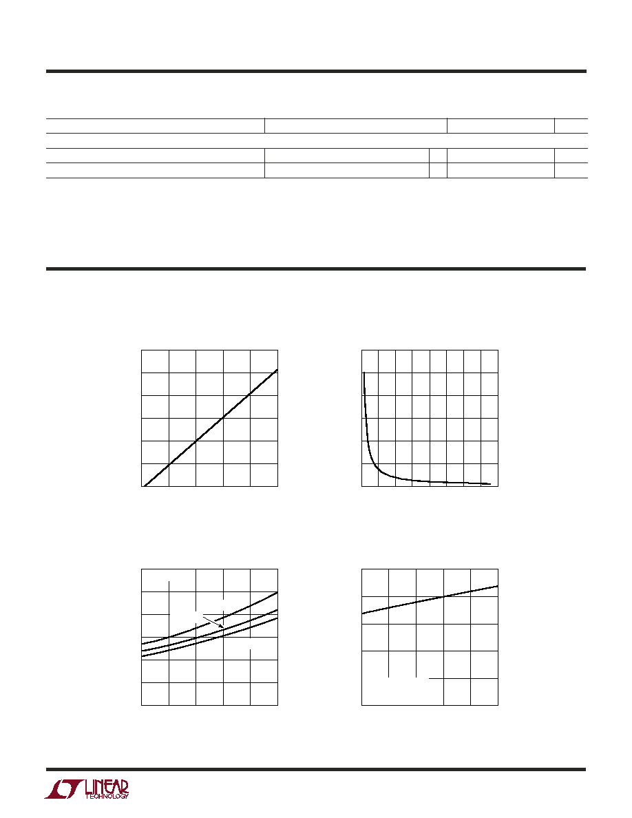
TYPICAL PERFOR A CE CHARACTERISTICS
U
W
I
LED
Dropout Voltage
vs LED Current
I
LED
vs R
SET
LED CURRENT (mA)
0
100
DROPOUT VOLTAGE (V)
300
200
400
500
3216 G01
0.12
0.10
0.08
0.06
0.04
0.02
0
TEMPERATURE (
°C)
40
15
OUTPUT RESISTANCE (
)
35
10
60
85
3216 G03
1.0
0.9
0.8
0.7
0.6
0.5
0.4
40
10
60
85
15
35
TEMPERATURE (
°C)
OUTPUT RESISTANCE (
)
5
4
3
2
1
0
3216 G05
R
SET
(k
)
I
LED
(mA)
1573 G02
600
500
400
300
200
100
0
0
100
200
250
50
150
300 350
400
V
IN
= 4.5V
V
IN
= 2.9V
I
CPO
= 100mA
V
IN
= 3.6V
V
IN
= 3.6V
C
IN
= C1 = C2 = 2.2
µF
C
CPO
= 4.7
µF
2x Mode Charge Pump
Open-Loop Output Resistance
(2V
IN
V
CPO
)/I
CPO
vs Temperature
1x Mode Charge Pump Open-Loop
Output Resistance vs Temperature
(T
A
= 25
°C unless otherwise specified)
ELECTRICAL CHARACTERISTICS
The
denotes the specifications which apply over the full operating
temperature range, otherwise specifications are at T
A
= 25
°C. V
IN
= 3.6V, C
IN
= C1 = C2 = 2.2
µF, C
CPO
= 4.7
µF.
PARAMETER
CONDITIONS
MIN
TYP
MAX
UNITS
I
SET
V
ISET
I
SET
= 50
µA
1.18
1.21
1.24
V
I
ISET
184
µA

LTC3214
4
3214f
3214 G12
V
CPO
50mV/DIV
A/C COUPLED
500ns/DIV
V
IN
= 3.6V
I
CPO
= 400mA
3214 G11
V
CPO
50mV/DIV
500ns/DIV
V
IN
= 3.6V
I
CPO
= 200mA
TYPICAL PERFOR A CE CHARACTERISTICS
U
W
1.5x Mode CPO Output Ripple
2x Mode CPO Output Ripple
Input Shutdown Current
vs Input Voltage
Oscillator Frequency
vs Supply Voltage
Efficiency vs V
IN
I
SET
/I
LED
Current Ratio
vs I
LED
Current
V
IN
(V)
2.9
EFFICIENCY (P
LED
/P
IN
) (%)
100
90
80
70
60
50
40
30
20
10
0
3.3
3.7
3.9
3215 G08
3.1
3.5
4.1
4.3
4.5
100mA
50mA
300mA
200mA
LED = AOT2015
V
F
= 2.9V TYP AT 100mA
I
LED
CURRENT (mA)
0
2700
CURRENT RATIO
2800
2900
3000
40
°C
85
°C
3100
200
100
300
400
500
3214 G09
3200
3300
25
°C
(T
A
= 25
°C unless otherwise specified)
I
LED
Current vs Input Voltage
4.5
4.0
3.5
3.0
2.5
2.0
1.5
1.0
0.5
0
INPUT SHUTDOWN CURRENT (
µ
A)
3214 G06
INPUT VOLTAGE (V)
2.9
4.5
3.3
3.7
4.1
3.1
3.5
3.9
4.3
T
A
= 85
°C
T
A
= 40
°C
T
A
= 25
°C
FREQUENCY (kHz)
910
900
870
890
880
860
850
840
830
3214 G07
SUPPLY VOLTAGE (V)
2.9
4.5
3.3
3.7
4.1
3.1
3.5
3.9
4.3
T
A
= 85
°C
T
A
= 40
°C
T
A
= 25
°C
V
IN
(V)
I
LED
(mA)
600
500
400
300
200
100
0
3214 G10
2.9
4.5
3.3
3.7
4.1
3.1
3.5
3.9
4.3
72.2k
36.6k
17.4k
11.8k
7.15k

LTC3214
5
3214f
U
U
U
PI FU CTIO S
BLOCK DIAGRA
W
GND
+
CONTROL
LOGIC
CPO
I
LED
GND
I
SET
V
IN
V
IN
EN
C1
+
C1
C2
+
C2
3214 BD
CURRENT
SOURCE
CONTROL
V
REF
VOLTAGE
CLAMP
58
0.11
250k
OSCILLATOR
MODE
CONTROL
2
10
1
8
3
4
11
5
9
6
7
C2
+
, C1
+
, C2
, C1
(Pins 1, 2, 8, 10): Charge Pump Flying
Capacitor Pins. A 2.2
µF X5R or X7R ceramic capacitor
should be connected from C1
+
to C1
and from C2
+
to
C2
.
CPO (Pin 3): Output. CPO is the output of the charge
pump. This pin may be enabled or disabled using the EN
input. A 4.7
µF X5R or X7R ceramic capacitor is required
from CPO to GND.
I
LED
(Pin 4): Input. I
LED
is the LED current sense pin. The
LED is connected between CPO (anode) and I
LED
(cath-
ode). The current into the I
LED
pin is set by a resistor
connected to the I
SET
pin and regulated internally.
I
SET
(Pin 5): LED Current Programming Resistor Pin. A
resistor connected between this pin and GND is used to set
the LED current level.
EN (Pin 6): Input. The EN pin is used to enable the part and
bring it into shutdown mode. An internal 250k
resistor
pulls this pin to GND when left floating.
V
IN
(Pin 7): Power. Supply voltage for the LTC3214. V
IN
should be bypassed with a 2.2
µF to 4.7µF low impedance
ceramic capacitor to GND.
GND (Pin 9): Charge Pump Ground. This pin should be
connected directly to a low impedance ground plane.
Exposed Pad (Pin 11): Control Signal Ground. This pad
must be soldered to a low impedance ground plane for
optimum thermal and electrical performance.