 | ÐлекÑÑоннÑй компоненÑ: LTC3217 | СкаÑаÑÑ:  PDF PDF  ZIP ZIP |
3217.pm65
LTC3217
1
3217f
FEATURES
DESCRIPTIO
U
Multi-LED Camera Light Supply for Cellphones/
DSCs/PDAs
Charge Pump Provides High Efficiency with
Automatic Mode Switching
Multimode Operation: 1x, 1.5x, 2x
Four Low Dropout LED Outputs
Up to 600mA Total Output Current
Independent Torch and Flash I
SET
and Enable Pins
Low Noise Constant Frequency Operation*
PWM Brightness Control via the EN2 Pin
Low Shutdown Current: 4
µA
Internal Soft-Start Limits Inrush Current During
Start-Up and Mode Switching
Open/Short LED Protection
No Inductors
(3mm x 3mm) 16-Lead QFN Plastic Package
600mA Low Noise
Multi-LED Camera Light
Charge Pump
The LTC
®
3217 is a low noise charge pump DC/DC con-
verter designed to power four high current LEDs. The
LTC3217 requires only four small ceramic capacitors and
two current set resistors to form a complete LED power
supply and current controller.
Built-in soft-start circuitry prevents excessive inrush cur-
rent during start-up and mode changes. High switching
frequency enables the use of small external capacitors.
Independent high and low current settings are programmed
by two external resistors. Shutdown mode and current
output levels are selected via two logic inputs.
The current through the LEDs is programmed via I
SET1
and
I
SET2
. In addition, the brightness can be controlled by
pulse width modulation of the EN2 pin.
The charge pump optimizes efficiency based on the volt-
age across the LED current sources. The part powers up
in 1x mode and will automatically switch to boost mode
whenever any enabled LED current source begins to enter
dropout. The first dropout switches the part into 1.5x
mode and a subsequent dropout switches the part into 2x
mode. The LTC3217 resets to 1x mode whenever the part
is shut down.
The LTC3217 is available in a low profile 16-lead (3mm
×
3mm
× 0.75mm) QFN package.
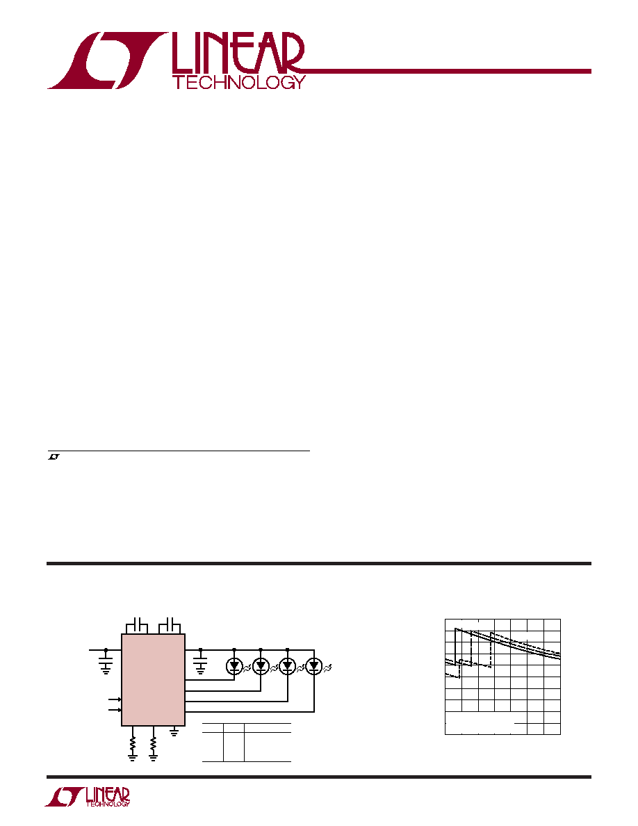
TYPICAL APPLICATIO
U
APPLICATIO S
U
C2
2.2
µF
C3
2.2
µF
C1
2.2
µF
V
BAT
19.6k
1%
6.49k
1%
LED1
LED2
LED3
LED4
GND
V
BAT
EN2
EN1
LTC3217
C1P
C1M C2P
C2M
C4
2.2
µF
AOT-2015HPW-1751B
3217 TA01
I
SET1
I
SET2
CPO
EN1 (TORCH)
EN2 (FLASH)
EN1
0
1
0
1
0 (SHUTDOWN)
25mA/LED
75mA/LED
100mA/LED
EN2
I
LED
0
0
1
1
, LTC and LT are registered trademarks of Linear Technology Corporation.
All other trademarks are the property of their respective owners.
*Protected by U.S. Patents, including 6411531
Efficiency vs V
BAT
V
BAT
(V)
3
0
EFFICIENCY (P
LED
/PIN) (%)
10
30
40
50
100
70
3.4
3.8
4
3217 G09
20
80
90
60
3.2
3.6
4.2
4.4
TOTAL OUTPUT CURRENT
P
LED
/PIN
LED = 2015 HPW AOT
100mA
200mA
400mA
LTC3217
2
3217f
V
BAT
, CPO to GND ....................................... 0.3V to 6V
EN1, EN2 .................................... 0.3V to (V
BAT
+ 0.3V)
I
CPO
(Note 2) ....................................................... 600mA
I
ILED1-4
(Note 3) .................................................. 150mA
CPO Short-Circuit Duration ............................. Indefinite
Operating Temperature Range (Note 4) ...40
°C to 85°C
Storage Temperature Range ..................65
°C to 125°C
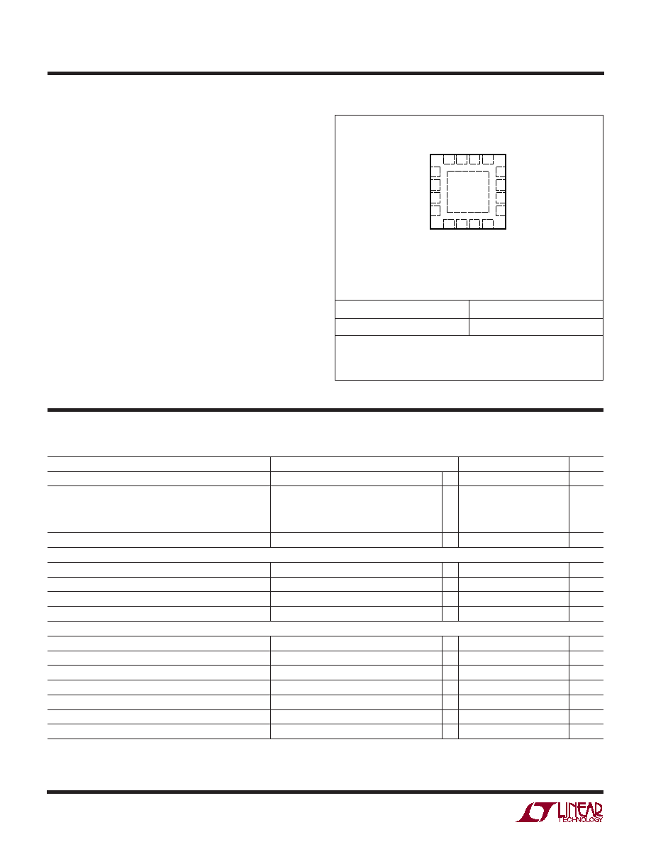
ORDER PART NUMBER
T
JMAX
= 125
°C,
JA
= 68
°C/W
EXPOSED PAD (PIN 17) IS GND MUST BE SOLDERED TO PCB
LTC3217EUD
ABSOLUTE AXI U
RATI GS
W
W
W
U
PACKAGE/ORDER I FOR ATIO
U
U
W
(Note 1)
Consult LTC Marketing for parts specified with wider operating temperature ranges.
QFN PART MARKING
LBTQ
16 15 14 13
5
6
7
8
TOP VIEW
17
UD PACKAGE
16-LEAD (3mm
× 3mm) PLASTIC QFN
9
10
11
12
4
3
2
1
C1P
CPO
EN1
LED1
C2M
EN2
I
SET2
I
SET1
C2P
V
BAT
C1M
GND1
LED2
LED3
LED4
GND2
ELECTRICAL CHARACTERISTICS
The
denotes the specifications which apply over the full operating
temperature range, otherwise specifications are at T
A
= 25
°C. V
BAT
= 3.6V, C1 = C2 = C3 = C4 = 2.2
µF, unless otherwise noted.
Order Options Tape and Reel: Add #TR
Lead Free: Add #PBF Lead Free Tape and Reel: Add #TRPBF
Lead Free Part Marking:
http://www.linear.com/leadfree/
PARAMETER
CONDITIONS
MIN
TYP
MAX
UNITS
V
BAT
Operating Voltage
2.9
4.5
V
I
VBAT
Operating Current
R
ISET1
= R
ISET2
= 20k, EN1 = EN2 = High
I
CPO
= 0mA, 1x Mode
1
mA
I
CPO
= 0mA, 1.5x Mode
4
mA
I
CPO
= 0mA, 2x Mode
6
mA
V
BAT
Shutdown Current
4
µA
LED 1-4 Current
LED Current Ratio (I
LED
/I
SET1/2
)
I
LED
= 25mA to 100mA
370
400
430
mA/mA
LED Dropout Voltage
Mode Switch Threshold, I
LED
= 100mA
330
mV
Mode Switching Delay
EN1 Only
2.5
ms
LED Current Matching
Any Two Outputs, I
LED
= 100mA
1
%
Charge Pump (CPO)
1x Mode Output Voltage
I
CPO
= 0mA
V
BAT
V
1.5x Mode Output Voltage
I
CPO
= 0mA
4.5
V
2x Mode Output Voltage
I
CPO
= 0mA
5.05
V
1x Mode Output Impedance
0.5
1.5x Mode Output Impedance
V
BAT
= 3.4V, V
CPO
4.6V (Note 5)
2.8
2x Mode Output Impedance
V
BAT
= 3.2V, V
CPO
5.1V (Note 5)
3.2
CLOCK Frequency
0.6
0.85
1.15
MHz
LTC3217
3
3217f
ELECTRICAL CHARACTERISTICS
TYPICAL PERFOR A CE CHARACTERISTICS
U
W
The
denotes the specifications which apply over the full operating
temperature range, otherwise specifications are at T
A
= 25
°C. V
BAT
= 3.6V, C1 = C2 = C3 = C4 = 2.2
µF, unless otherwise noted.
Note 1: Absolute Maximum Ratings are those values beyond which the life of
a device may become impaired.
Note 2: Based on charge pump long-term current density limitations.
Assumes an operating duty cycle of
10% under absolute maximum
conditions for durations less than 10 seconds. Maximum current for
continuous operation is 300mA.
Note 3: Based on LED current source long-term current density limitations.
Assumes an operating duty cycle of
10% under absolute maximum
conditions for durations less than 10 seconds. Maximum current for
continuous operation is 100mA.
Note 4: The LTC3217E is guaranteed to meet performance specifications
from 0
°C to 70°C. Specifications over the 40°C to 85°C ambient operating
temperature range are assured by design, characterization and correlation
with statistical process controls.
Note 5: 1.5x mode output impedance is defined as (1.5V
BAT
V
CPO
)/I
OUT
.
2x mode output impedance is defined as (2V
BAT
V
CPO
)/I
OUT
.
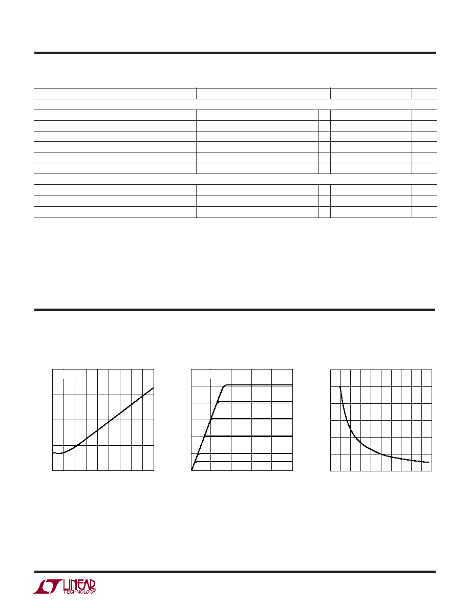
LED Dropout Voltage
vs LED Current
LED CURRENT (mA)
10
0
LED DROPOUT VOLTAGE (mV)
100
200
300
400
20
30
40
50
3217 G01
60
70
80
90 100
V
BAT
= 3.6V
LED PIN VOLTAGE (V)
0
0
LED PIN CURRENT (mA)
20
40
60
80
100
120
0.2
0.4
0.6
0.8
3217 G02
1.0
V
BAT
= 3.6V
R
ISET
(k
)
0
I
LED
(mA)
40
80
120
20
60
100
10
20
30
40
3217 G03
50
5
0
15
25
35
45
LED Pin Current
vs LED Pin Voltage
I
LED
vs R
ISET
PARAMETER
CONDITIONS
MIN
TYP
MAX
UNITS
EN1, EN2
Low Level Input Voltage (V
IL
)
0.4
V
High Level Input Voltage (V
IH
)
1.4
V
Input Current (I
IH
)
7
30
µA
Input Current (I
IL
)
1
1
µA
Minimum PWM On-Time
EN2 Only
50
µs
Maximum PWM Off-Time
EN2 to Remain Enabled, EN1 = Low
1
ms
I
SET1
, I
SET2
V
ISET1
,
ISET2
I
LED1-4
= 12.5mA
1.175
1.215
1.255
V
I
ISET1
,
ISET2
Current Range
31.25
375
µA
I
ISET1
,
ISET2
Short-Circuit Current
800
µA
T
A
= 25
°C unless otherwise noted.
LTC3217
4
3217f
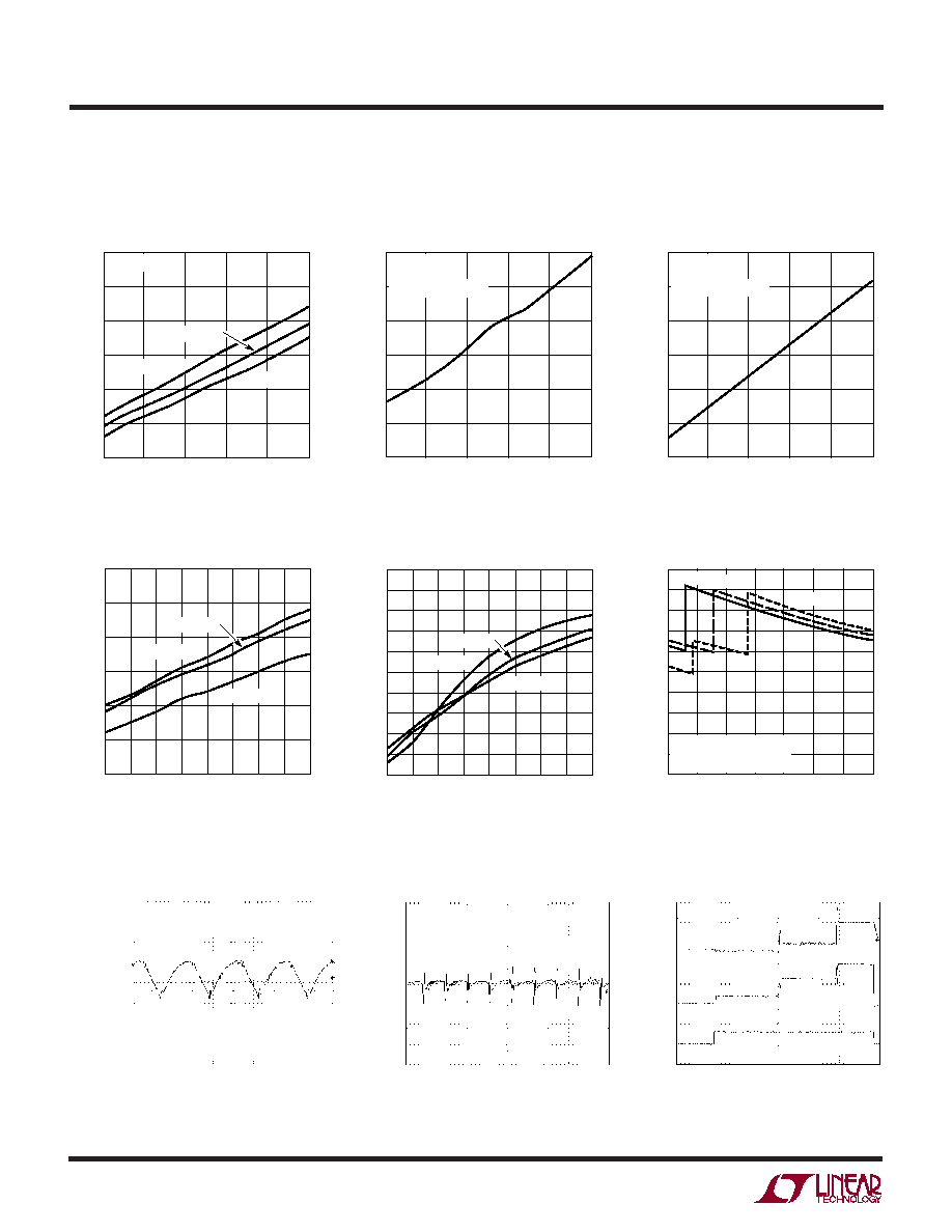
V
BAT
Shutdown Current
vs V
BAT
Voltage
Oscillator Frequency
vs Supply Voltage
Efficiency vs V
BAT
V
BAT
VOLTAGE (V)
2.9
1.5
V
BAT
SHUTDOWN CURRENT (
µ
A)
2.5
3.5
4.5
5.5
3.3
3.7
4.1
4.5
3217 G07
6.5
7.5
3.1
3.5
3.9
4.3
T
A
= 85
°C
T
A
= 25
°C
T
A
= 40
°C
V
BAT
SUPPLY VOLTAGE (V)
2.9
880
FREQUENCY (kHz)
890
910
920
930
980
950
3.3
3.7
3.9
3217 G08
900
960
970
940
3.1
3.5
4.1
4.3
4.5
T
A
= 40
°C
T
A
= 25
°C
T
A
= 85
°C
V
BAT
(V)
3
0
EFFICIENCY (P
LED
/PIN) (%)
10
30
40
50
100
70
3.4
3.8
4
3217 G09
20
80
90
60
3.2
3.6
4.2
4.4
TOTAL OUTPUT CURRENT
P
LED
/PIN
LED = 2015 HPW AOT
100mA
200mA
400mA
1.5x Mode CPO Output Ripple
2x Mode CPO Output Ripple
Charge Pump Mode Switching
and Input Current to Ground
(400mA Load)
V
CPO
50mV/DIV
AC COUPLED
500ns/DIV
V
BAT
= 3.6V
I
CPO
= 400mA
C
CPO
= 2.2
µF
3217 G10
V
CPO
20mV/DIV
AC COUPLED
500ns/DIV
3217 G11
V
BAT
= 3.6V
I
CPO
= 400mA
C
CPO
= 2.2
µF
V
CPO
1V/DIV
I
VBAT
500mA/DIV
0
EN1
5V/DIV
1ms/DIV
1x
NO LOAD
1x
DROPOUT
DROPOUT
1.5x
2x
(5V)
V
IN
= 3.6V
3217 G12
1x Mode Switch Resistance
vs Temperature
1.5x Mode Charge Pump Open-Loop
Output Resistance vs Temperature
(1.5V
BAT
V
CPO
)/I
CPO
TEMPERATURE (
°C)
40
0.35
SWITCH RESISTANCE (
)
0.40
0.45
0.50
0.55
0.60
0.65
15
10
35
60
3217 G04
85
I
CPO
= 200mA
V
BAT
= 3.3V
V
BAT
= 3.9V
V
BAT
= 3.6V
TEMPERATURE (
°C)
40
2.0
SWITCH RESISTANCE (
)
2.2
2.4
2.6
2.8
3.0
3.2
15
10
35
60
3217 G05
85
V
BAT
= 3V
V
CPO
= 4.2V
C2 = C3 = C4 = 2.2
µF
2x Mode Charge Pump Open-Loop
Output Resistance vs Temperature
(2V
BAT
V
CPO
)/I
CPO
TEMPERATURE (
°C)
40
2.6
SWITCH RESISTANCE (
)
2.8
3.0
3.2
3.4
3.6
3.8
15
10
35
60
3217 G06
85
V
BAT
= 3V
V
CPO
= 4.8V
C2 = C3 = C4 = 2.2
µF
TYPICAL PERFOR A CE CHARACTERISTICS
U
W
T
A
= 25
°C unless otherwise noted.
LTC3217
5
3217f
U
U
U
PI FU CTIO S
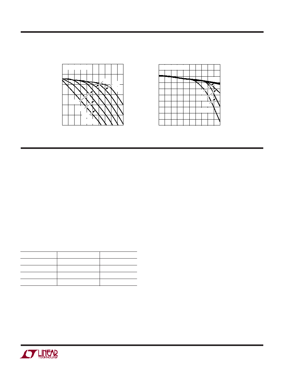
1.5x Mode CPO Voltage
vs Load Current
LOAD CURRENT (mA)
3.6
CPO VOLTAGE (V) 4.0
4.4
4.8
3.8
4.2
4.6
100
200
300
400
3217 G13
500
0
C2 = C3 = C4 = 2.2
µF
V
BAT
= 3V
3.2V
3.3V
3.6V
3.1V
3.5V
3.4V
2x Mode CPO Voltage
vs Load Current
LOAD CURRENT (mA)
0
CPO VOLTAGE (V)
4.8
5.0
5.2
400
3217 G14
4.6
4.4
4.7
4.9
5.1
4.5
4.3
4.2
100
200
300
500
C2 = C3 = C4 = 2.2
µF
V
BAT
= 3V
3.1V
3.2V
3.3V
3.6V
C1P, C2P, C1M, C2M (Pins 1, 16, 14, 12): Charge Pump
Flying Capacitor Pins. A 2.2
µF X7R or X5R ceramic capaci-
tor should be connected from C1P to C1M and C2P to C2M.
CPO (Pin 2): Output of the charge pump used to power all
LEDs. This pin is enabled or disabled using the EN1 and
EN2 inputs. A 2.2
µF X5R or X7R ceramic capacitor should
be connected to ground.
EN1, EN2 (Pins 3, 11): Inputs. The EN1 and EN2 pins are
used to select which current level is being supplied to the
LEDs, as well as to put the part into shutdown mode. The
truth table for these pins is as follows:
Truth Table
EN1
EN2
MODE
0
0
Shutdown
1
0
Low Current
0
1
High Current
1
1
Low + High Current
EN2 can be used for PWM of the LED currents. For proper
operation, the minimum pulse width should be 50
µs and
the maximum low time should be 1ms if EN1 is low. If EN1
is high then the 1ms low time limitation does not apply.
LED1, LED2, LED3, LED4 (Pins 4, 5, 6, 7): LED1 to LED4
are the current source outputs. Each LED is connected in
between CPO (anodes) and LED1 4 (cathodes). The
current to each LED output is set via the EN1 and EN2
inputs, and the programming resistors connected from
I
SET1
and I
SET2
to GND. Any of the four LED outputs can
be disabled by connecting the output directly to CPO.
10
µA of current will flow through each directly connected
LED output. For single LED applications, all four LED pins
may be tied together and will accurately share current.
GND2 (Pin 8): Analog Ground. This pin should be
connected directly to a low impedance ground plane.
I
SET1
/I
SET2
(Pins 9, 10): LED Current Programming
Resistor Pins. The I
SET1
and I
SET2
pins will servo to 1.22V.
Resistors connected between each of these pins and GND
are used to set the high and low LED current levels.
Connecting a resistor 2k or less will cause the LTC3217 to
enter over-current shutdown.
GND1 (Pin 13): Charge Pump Ground. This pin should be
connected directly to a low impedance ground plane.
V
BAT
(Pin 15): Supply Voltage. This pin should be
bypassed with a 2.2
µF, or greater low ESR ceramic
capacitor.
Exposed Pad (Pin 17): This pad should be connected
directly to a low impedance ground plane for optimal
thermal and electrical performance.
TYPICAL PERFOR A CE CHARACTERISTICS
U
W
T
A
= 25
°C unless otherwise noted.