3250-1.5f
LTC3250-1.5
1
3250f
DESCRIPTIO
U
APPLICATIO S
U
FEATURES
TYPICAL APPLICATIO
U
s
Handheld Computers
s
Cellular Phones
s
Digital Cameras
s
Handheld Medical Instruments
s
Low Power DSP Supplies
s
3.1V to 5.5V Input Voltage Range
s
No Inductors
s
Li-Ion (3.6V) to 1.5V with 81% Efficiency
s
Low Noise Constant Frequency Operation
s
Output Voltage: 1.5V
±
4%
s
Output Current: 250mA
s
Shutdown Disconnects Load from V
IN
s
Low Operating Current: I
Q
= 35
µ
A
s
Low Shutdown Current: I
SD
< 1
µ
A
s
Oscillator Frequency = 1.5MHz
s
Soft-Start Limits Inrush Current at Turn-On
s
Short-Circuit and Overtemperature Protected
s
Low Profile (1mm) ThinSOT
TM
Package
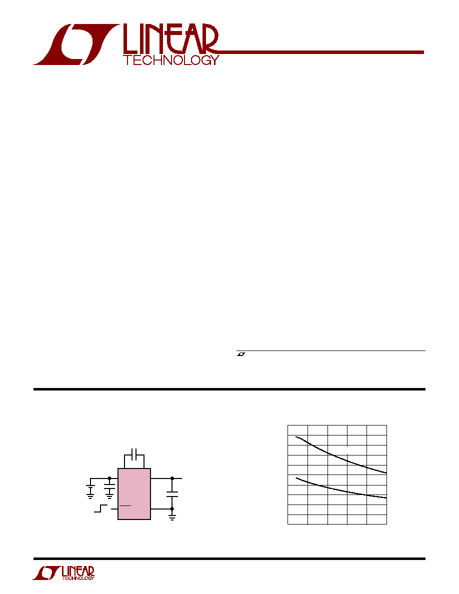
High Efficiency, Low Noise,
Inductorless Step-Down
DC/DC Converter
3250 TA1a
LTC3250-1.5
V
IN
V
IN
3.2V TO 4.2V
SHDN
C
+
C
V
OUT
4
3
2
1
5
6
GND
ON
OFF
1
µ
F
4.7
µ
F
V
OUT
= 1.5V
±
4%
100mA
Li-Ion
1
µ
F
Efficiency vs Input Voltage
(I
OUT
= 100mA)
The LTC
®
3250-1.5 is a charge pump step-down DC/DC
converter that produces a 1.5V regulated output from a
3.1V to 5.5V input. The part uses switched capacitor
fractional conversion to achieve a typical efficiency in-
crease of 50% over that of a linear regulator. No inductors
are required.
A unique constant frequency architecture provides a low
noise regulated output as well as lower input noise
than conventional charge pump regulators.* High
frequency operation (f
OSC
= 1.5MHz) simplifies filtering
to further reduce conducted noise. The part also uses
Burst Mode
®
operation to improve efficiency at light loads.
Low operating current (35
µ
A with no load, <1
µ
A in
shutdown) and low external parts count (three small
ceramic capacitors) make the LTC3250-1.5 ideally suited
for space constrained battery powered applications. The
part is short-circuit and overtemperature protected, and is
available in a low profile (1mm) 6-pin ThinSOT package.
, LTC and LT are registered trademarks of Linear Technology Corporation.
Burst Mode is a registered trademark of Linear Technology Corporation.
ThinSOT is a trademark of Linear Technology Corporation.
*U.S. Patent #6, 411, 531
V
IN
(V)
3.0
3.5
4.0
4.5
5.0
5.5
EFFICIENCY (%)
3250 TA01b
100
90
80
70
60
50
40
30
20
10
0
LDO
LTC3250-1.5
Li-Ion to 1.5V Output with Shutdown
LTC3250-1.5
2
3250f
V
IN
to GND ................................................... 0.3V to 6V
SHDN to GND ............................... 0.3V to (V
IN
+ 0.3V)
I
OUT
(Note 2) ....................................................... 350mA
Operating Temperature Range (Note 3) .. 40
°
C to 85
°
C
Storage Temperature Range ................ 65
°
C to 150
°
C
Lead Temperature (Soldering, 10 sec).................. 300
°
C
ORDER PART
NUMBER
S6 PART MARKING
T
JMAX
= 150
°
C,
JA
= 230
°
C/W
LTZE
LTC3250ES6-1.5
ABSOLUTE AXI U
RATI GS
W
W
W
U
PACKAGE/ORDER I FOR ATIO
U
U
W
(Note 1)
ELECTRICAL CHARACTERISTICS
The
q
denotes the specifications which apply over the full operating
temperature range, otherwise specifications are at T
A
= 25
°
C. V
IN
= 3.6V, C
FLY
= 1
µ
F, C
IN
= 1
µ
F, C
OUT
= 4.7
µ
F unless otherwise noted.
SYMBOL
PARAMETER
CONDITIONS
MIN
TYP
MAX
UNITS
V
IN
Operating Voltage
q
3.1
5.5
V
V
OUT
I
OUT
50mA
q
1.44
1.5
1.56
V
I
OUT
100mA 3.2V
V
IN
5.5V
q
1.44
1.5
1.56
V
I
OUT
250mA 3.5V
V
IN
5V
1.44
1.5
1.56
V
I
IN
Operating Current
I
OUT
= 0mA
q
35
60
µ
A
Shutdown Current
SHDN = 0V
q
0.01
1
µ
A
V
RB
Burst Mode Operation Output Ripple
12
mV
P-P
V
RC
Continuous Mode Output Ripple
4
mV
P-P
f
OSC
Switching Frequency
q
1.2
1.5
1.8
MHz
V
IH
SHDN Input Hi Voltage
q
1.2
0.8
V
V
IL
SHDN Input Low Voltage
q
0.8
0.4
V
I
IH
SHDN Input Current
SHDN = V
IN
q
1
1
µ
A
I
IL
SHDN Input Current
SHDN = 0V
q
1
1
µ
A
t
ON
Turn On Time
R
LOAD
= 6
0.8
ms
Load Regulation
0
I
OUT
250mA
0.15
mV/mA
Line Regulation
0
I
OUT
250mA
0.2
%/V
R
OL
Open-Loop Output Impedance
V
IN
= 3.1V, I
OUT
= 250mA (Note 4)
1.0
Consult LTC Marketing for parts specified with wider operating temperature ranges.
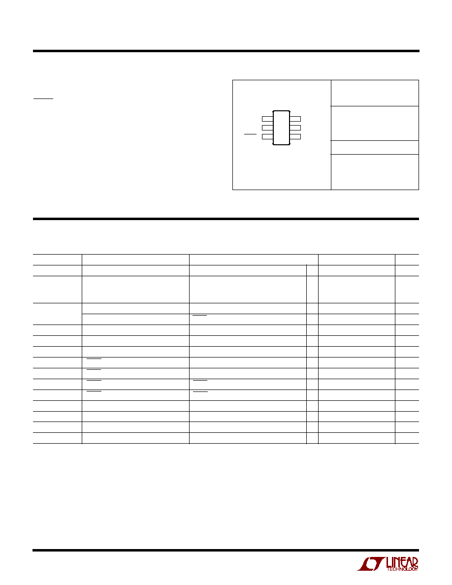
6 C
+
5 V
OUT
4 C
V
IN
1
TOP VIEW
S6 PACKAGE
6-LEAD PLASTIC SOT-23
GND 2
SHDN 3
Note 1: Absolute Maximum Ratings are those values beyond which the life
of a device may be impaired.
Note 2: Based on long term current density limitations.
Note 3: The LTC3250-1.5E is guaranteed to meet specified performance
from 0
°
C to 70
°
C. Specifications over the 40
°
C and 85
°
C operating
temperature range are assured by design characterization and correlation
with statistical process controls.
Note 4: Output not in regulation; R
OL
= (V
IN
/2 - V
OUT
)/I
OUT
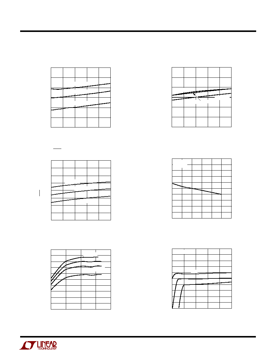
LTC3250-1.5
3
3250f
No Load Supply Current vs
Supply Voltage
Output Voltage vs Supply Voltage
Output Voltage vs Load Current
Oscillator Frequency vs
Supply Voltage
Efficiency vs Output Current
V
SHDN
Threshold Voltage vs
Supply Voltage
TYPICAL PERFOR A CE CHARACTERISTICS
U
W
V
IN
(V)
3.0
I
IN
(
µ
A)
50
45
40
35
30
25
20
5.0
3250 G01
3.5
4.0
4.5
5.5
T
A
= 40
°
C
T
A
= 25
°
C
T
A
= 85
°
C
V
IN
(V)
3.0
FREQUENCY (MHz)
1.8
1.7
1.6
1.5
1.4
1.3
1.2
5.0
3250 G02
3.5
4.0
4.5
5.5
T
A
= 40
°
C
T
A
= 25
°
C
T
A
= 85
°
C
V
IN
(V)
3.0
V
SHDN
(mV)
1200
1100
1000
900
800
700
600
500
400
5.0
3250 G03
3.5
4.0
4.5
5.5
T
A
= 40
°
C
T
A
= 25
°
C
T
A
= 85
°
C
I
OUT
(mA)
0
V
OUT
(V)
50
100
150
200
3250 G04
250
1.60
1.58
1.56
1.54
1.52
1.50
1.48
1.46
1.44
1.42
1.40
300
V
IN
= 3.6V
T
A
= 25
°
C
I
OUT
(mA)
1
0.1
EFFICIENCY (%)
1000
3250 G05
10
100
100
90
80
70
60
50
40
30
20
10
0
V
IN
= 3.6V
V
IN
= 3.3V
V
IN
= 4V
V
IN
= 5V
V
IN
(V)
3.0
V
OUT
(V)
1.60
1.58
1.56
1.54
1.52
1.50
1.48
1.46
1.44
1.42
1.40
5.0
3250 G06
3.5
4.0
4.5
5.5
0mA
250mA
100mA
T
A
= 25
°
C
LTC3250-1.5
4
3250f
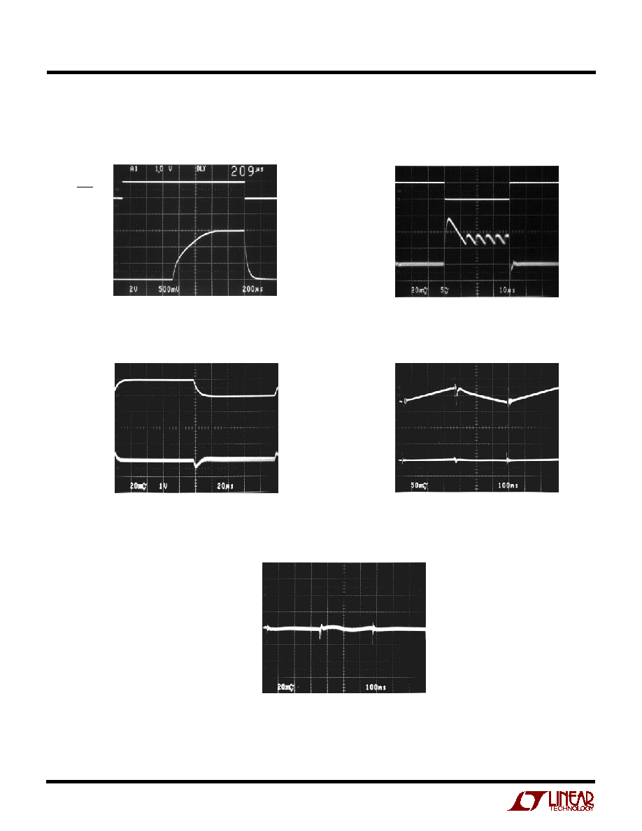
Output Voltage Soft-Start and
Shutdown
Output Current Transient
Response
Line Transient Response
TYPICAL PERFOR A CE CHARACTERISTICS
U
W
Output Voltage Ripple
Input Voltage Ripple vs Input
Capacitor
250mA
15mA
I
OUT
V
OUT
20mV/DIV
AC
V
IN
= 3.6V
3250 G08
3250 G09
4.5V
3.5V
V
IN
V
OUT
20mV/DIV
AC
I
OUT
= 200mA
V
IN
50mV/DIV
AC
V
IN
50mV/DIV
AC
I
OUT
= 250mA
R
SOURCE
= 0.2
3250 G10
C
I
= 1
µ
F
C
I
= 10
µ
F
V
OUT
20mV/DIV
AC
3250 G11
C
OUT
= 4.7
µ
F 1X5R16.3V
I
OUT
= 250mA
V
IN
= 3.6V
HI
LOW
SHDN
V
OUT
500mV/DIV
R
L
= 6
V
IN
= 3.6V
3250 G07
LTC3250-1.5
5
3250f
V
IN
(Pin 1): Input Supply Voltage. Operating V
IN
may be
between 3.1V and 5.5V. Bypass V
IN
with a
1
µ
F low ESR
ceramic capacitor.
GND (Pin 2): Ground. Connect to a ground plane for best
performance.
SHDN (Pin 3): Active Low Shutdown Input. A low voltage
on SHDN disables the LTC3250-1.5. SHDN must not be
allowed to float.
C
(Pin 4): Flying Capacitor Negative Terminal
V
OUT
(Pin 5): Regulated Output Voltage. V
OUT
is discon-
nected from V
IN
during shutdown. Bypass V
OUT
with a
4.7
µ
F low ESR ceramic capacitor (2.5
µ
F min, ESR
<100m
).
C
+
(Pin 6): Flying Capacitor Positive Terminal.
U
U
U
PI FU CTIO S
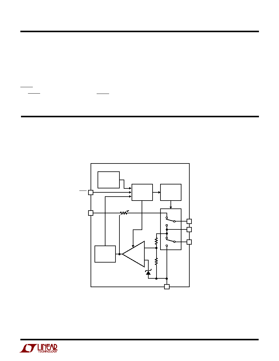
BLOCK DIAGRA
W
3250 BD
+
3
1
2
6
5
4
THERMAL
SHUTDOWN
(>160
°
C)
SWITCH
CONTROL
AND
SOFT-START
1.5MHz
OSCILLATOR
CHARGE
PUMP
BURST
DETECT
CIRCUIT
GND
SHDN
V
IN
C
+
C
V
OUT
LTC3250-1.5
V
REF